EP1519475A1 - Ein Sanftschaltender Stromwandler mit Klemm - Google Patents
Ein Sanftschaltender Stromwandler mit Klemm Download PDFInfo
- Publication number
- EP1519475A1 EP1519475A1 EP03021511A EP03021511A EP1519475A1 EP 1519475 A1 EP1519475 A1 EP 1519475A1 EP 03021511 A EP03021511 A EP 03021511A EP 03021511 A EP03021511 A EP 03021511A EP 1519475 A1 EP1519475 A1 EP 1519475A1
- Authority
- EP
- European Patent Office
- Prior art keywords
- power
- soft switching
- diode
- capacitor
- drive signal
- Prior art date
- Legal status (The legal status is an assumption and is not a legal conclusion. Google has not performed a legal analysis and makes no representation as to the accuracy of the status listed.)
- Withdrawn
Links
- 239000003990 capacitor Substances 0.000 claims abstract description 35
- 238000010586 diagram Methods 0.000 description 4
- BNPSSFBOAGDEEL-UHFFFAOYSA-N albuterol sulfate Chemical compound OS(O)(=O)=O.CC(C)(C)NCC(O)C1=CC=C(O)C(CO)=C1.CC(C)(C)NCC(O)C1=CC=C(O)C(CO)=C1 BNPSSFBOAGDEEL-UHFFFAOYSA-N 0.000 description 1
- 238000007796 conventional method Methods 0.000 description 1
- 230000007812 deficiency Effects 0.000 description 1
- 230000005669 field effect Effects 0.000 description 1
- 229910044991 metal oxide Inorganic materials 0.000 description 1
- 150000004706 metal oxides Chemical class 0.000 description 1
- 230000003071 parasitic effect Effects 0.000 description 1
- 239000004065 semiconductor Substances 0.000 description 1
- 230000001960 triggered effect Effects 0.000 description 1
Images




Classifications
-
- H—ELECTRICITY
- H02—GENERATION; CONVERSION OR DISTRIBUTION OF ELECTRIC POWER
- H02M—APPARATUS FOR CONVERSION BETWEEN AC AND AC, BETWEEN AC AND DC, OR BETWEEN DC AND DC, AND FOR USE WITH MAINS OR SIMILAR POWER SUPPLY SYSTEMS; CONVERSION OF DC OR AC INPUT POWER INTO SURGE OUTPUT POWER; CONTROL OR REGULATION THEREOF
- H02M1/00—Details of apparatus for conversion
- H02M1/44—Circuits or arrangements for compensating for electromagnetic interference in converters or inverters
-
- H—ELECTRICITY
- H02—GENERATION; CONVERSION OR DISTRIBUTION OF ELECTRIC POWER
- H02M—APPARATUS FOR CONVERSION BETWEEN AC AND AC, BETWEEN AC AND DC, OR BETWEEN DC AND DC, AND FOR USE WITH MAINS OR SIMILAR POWER SUPPLY SYSTEMS; CONVERSION OF DC OR AC INPUT POWER INTO SURGE OUTPUT POWER; CONTROL OR REGULATION THEREOF
- H02M3/00—Conversion of DC power input into DC power output
- H02M3/02—Conversion of DC power input into DC power output without intermediate conversion into AC
- H02M3/04—Conversion of DC power input into DC power output without intermediate conversion into AC by static converters
- H02M3/10—Conversion of DC power input into DC power output without intermediate conversion into AC by static converters using discharge tubes with control electrode or semiconductor devices with control electrode
- H02M3/145—Conversion of DC power input into DC power output without intermediate conversion into AC by static converters using discharge tubes with control electrode or semiconductor devices with control electrode using devices of a triode or transistor type requiring continuous application of a control signal
- H02M3/155—Conversion of DC power input into DC power output without intermediate conversion into AC by static converters using discharge tubes with control electrode or semiconductor devices with control electrode using devices of a triode or transistor type requiring continuous application of a control signal using semiconductor devices only
- H02M3/156—Conversion of DC power input into DC power output without intermediate conversion into AC by static converters using discharge tubes with control electrode or semiconductor devices with control electrode using devices of a triode or transistor type requiring continuous application of a control signal using semiconductor devices only with automatic control of output voltage or current, e.g. switching regulators
- H02M3/158—Conversion of DC power input into DC power output without intermediate conversion into AC by static converters using discharge tubes with control electrode or semiconductor devices with control electrode using devices of a triode or transistor type requiring continuous application of a control signal using semiconductor devices only with automatic control of output voltage or current, e.g. switching regulators including plural semiconductor devices as final control devices for a single load
-
- H—ELECTRICITY
- H02—GENERATION; CONVERSION OR DISTRIBUTION OF ELECTRIC POWER
- H02M—APPARATUS FOR CONVERSION BETWEEN AC AND AC, BETWEEN AC AND DC, OR BETWEEN DC AND DC, AND FOR USE WITH MAINS OR SIMILAR POWER SUPPLY SYSTEMS; CONVERSION OF DC OR AC INPUT POWER INTO SURGE OUTPUT POWER; CONTROL OR REGULATION THEREOF
- H02M3/00—Conversion of DC power input into DC power output
- H02M3/22—Conversion of DC power input into DC power output with intermediate conversion into AC
- H02M3/24—Conversion of DC power input into DC power output with intermediate conversion into AC by static converters
- H02M3/28—Conversion of DC power input into DC power output with intermediate conversion into AC by static converters using discharge tubes with control electrode or semiconductor devices with control electrode to produce the intermediate AC
- H02M3/325—Conversion of DC power input into DC power output with intermediate conversion into AC by static converters using discharge tubes with control electrode or semiconductor devices with control electrode to produce the intermediate AC using devices of a triode or a transistor type requiring continuous application of a control signal
- H02M3/335—Conversion of DC power input into DC power output with intermediate conversion into AC by static converters using discharge tubes with control electrode or semiconductor devices with control electrode to produce the intermediate AC using devices of a triode or a transistor type requiring continuous application of a control signal using semiconductor devices only
- H02M3/33569—Conversion of DC power input into DC power output with intermediate conversion into AC by static converters using discharge tubes with control electrode or semiconductor devices with control electrode to produce the intermediate AC using devices of a triode or a transistor type requiring continuous application of a control signal using semiconductor devices only having several active switching elements
Definitions
- the present invention relates to a soft switching clamp, in particular to an application of soft-switching converter circuit to a PWM converter to recover ringing energy and suppress EMI when the switches of the power converter is turned off, and also do not increase switching loss when the switches are turned back on.
- a PWM converter typically use the power metal-oxide semiconductor field-effect transistors (MOSFETs) as switch.
- MOSFETs power metal-oxide semiconductor field-effect transistors
- the common practice to reduce EMI level is to install a clamping capacitor between the drain and the source of the switch to moderate the rate of change of voltage, and suppress EMI.
- the main object of the present invention is to provide a soft switching clamp installable on power switches of a power converter, that not only can moderate the rate of change of voltage when the power switches of the power converter are turned off, but are also do not increase the switching loss when the power switches are turned back on.
- the instrumentalities of the present invention to create the soft switching clamp comprising:
- the capacitor When the power switch is turned off, the capacitor accumulates energy through the existing path of the first diode.
- the power switch is turned on again, as the first diode is reverse biased, and the stored energy is released through the circuit made up by the second inductor, the reset switch and the second diode.
- the power switch is again turned off, as the capacitor is charged through the first diode, the voltage of the power switch will be increased moderately, thus being able to suppress EMI.
- the present invention provides a soft switching clamp installable on the power switches of a PWM converter to recover ringing energy and suppress EMI.
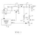
- An implementation of the present invention on a boost converter is demonstrated in Fig. 1, where the structure of the power converter, in accordance with the present invention, includes a power switch (10) (only one is shown for simplicity of illustration, although actually there is maybe more than one power switch in a power converter), a PWM drive circuit (20), and a clamping circuit formed by a first diode (31), a capacitor (32), a second diode (33), a reset switch (34), and a second inductor (35).
- the source terminal of the power switch is grounded, and the drain terminal is connected to the input voltage through the first inductor (11), and at the same time, the drain terminal of the power switch is also connected to the output voltage through an output diode (12).
- the output voltage feeds back a control signal to a PWM controller (13) for control the output voltage.
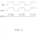
- the PWM controller (13) generate a PWM signal to the PWM driver circuit (20) to generate two drive signals (DRV-M) (DRV-S), wherein the first drive signal (DRV-M) is used to control the power switch (10) and the second drive signal (DRV-S) is used to drive the reset switch (34) (the waveform diagram of the two drive signals (DRV-M) (DRV-S) generated by the PWM driver circuit (20) is shown in Fig. 3).
- the present invention creates a clamping circuit to replace the conventional clamping capacitor parallel connected between the drain and source terminals of the power switch (10) of a power converter, supported by the following components during operation of the power switch (10):
- the above circuit is implemented by one preferred embodiment of the present invention.
- the second diode (33) can be connected to the power input instead of the power output, whilst other connections remain the same as in the previous example.
- the waveform diagram of the two drive signals (DRV-M) (DRV-S) generated by the PWM driver circuit (20) is shown in Fig. 3.
- the first drive signal (DRV-M) controlling the power switch (10) is either in step with the output signal of the PWM controller (13) or obtained directly from the output of the PWM controller (13).
- the second drive signal (DRV-S) uses one or more pulse signals, when the first drive signal (DRV-M) is enabled, to drive the reset switch (34).
- the control signals in Fig. 4 are used to drive the power converter in the first embodiment of the invention. Their circuit actions can be analyzed in stages in the order of time sequence. For simplicity in the illustration, the parasitic capacitance of the both switches (10) is largely ignored.
- the power switch (10) and the reset switch (34) are both turned off, and the input voltage through the first inductor (11) and the first diode (31) is used to charge the capacitor (32), until the voltage reaches the same level as the input voltage.
- a boost circuit is formed by the reset switch (34), the second inductor (35), and the second diode (33), which causes the stored energy in the capacitor (32) to be transferred to the voltage output, and the voltage of the capacitor (32) drops to a certain value.
- the above illustration explains the operation of the clamping circuit as implemented by the first embodiment. If the circuit is modified as in Fig. 2, the only difference in circuit action is that stored energy in the capacitor (32) is fed back to the power input instead of the power output.
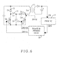
- the present invention is not only applicable to boost converters, but is also suitable for forward converters and flyback converters, as shown by the different implementations in Figs. 5, 6.
- the present design is not only able to moderate the rate of change of voltage when the switches are turned off, it can also reverse recover the energy of the capacitor to the power input or power output. Furthermore, the present design does not increase switching loss for a power converter when the power switches are turned on again.
Landscapes
- Engineering & Computer Science (AREA)
- Power Engineering (AREA)
- Physics & Mathematics (AREA)
- Electromagnetism (AREA)
- Dc-Dc Converters (AREA)
Priority Applications (1)
| Application Number | Priority Date | Filing Date | Title |
|---|---|---|---|
| EP03021511A EP1519475A1 (de) | 2003-09-24 | 2003-09-24 | Ein Sanftschaltender Stromwandler mit Klemm |
Applications Claiming Priority (1)
| Application Number | Priority Date | Filing Date | Title |
|---|---|---|---|
| EP03021511A EP1519475A1 (de) | 2003-09-24 | 2003-09-24 | Ein Sanftschaltender Stromwandler mit Klemm |
Publications (1)
| Publication Number | Publication Date |
|---|---|
| EP1519475A1 true EP1519475A1 (de) | 2005-03-30 |
Family
ID=34178484
Family Applications (1)
| Application Number | Title | Priority Date | Filing Date |
|---|---|---|---|
| EP03021511A Withdrawn EP1519475A1 (de) | 2003-09-24 | 2003-09-24 | Ein Sanftschaltender Stromwandler mit Klemm |
Country Status (1)
| Country | Link |
|---|---|
| EP (1) | EP1519475A1 (de) |
Cited By (4)
| Publication number | Priority date | Publication date | Assignee | Title |
|---|---|---|---|---|
| CN100421338C (zh) * | 2005-08-01 | 2008-09-24 | 台达电子工业股份有限公司 | 具脉宽调制限幅控制器的升压电路及其控制方法 |
| DE102013104376B3 (de) * | 2013-04-30 | 2014-09-25 | Sma Railway Technology Gmbh | Hochsetzsteller mit Resonanzkreis |
| WO2014177717A1 (de) | 2013-05-03 | 2014-11-06 | Sma Solar Technology Ag | Hoch- oder tiefsetzsteller mit entlastungskondensator |
| CN113595392A (zh) * | 2021-08-20 | 2021-11-02 | 南通大学 | 一种具有较高升压能力的三端口变换器及其控制方法 |
Citations (2)
| Publication number | Priority date | Publication date | Assignee | Title |
|---|---|---|---|---|
| US5414613A (en) * | 1993-08-20 | 1995-05-09 | Rem Technologies, Incorporated | Soft switching active snubber for semiconductor circuit operated in discontinuous conduction mode |
| US20030095421A1 (en) * | 2000-05-23 | 2003-05-22 | Kadatskyy Anatoly F. | Power factor correction circuit |
-
2003
- 2003-09-24 EP EP03021511A patent/EP1519475A1/de not_active Withdrawn
Patent Citations (2)
| Publication number | Priority date | Publication date | Assignee | Title |
|---|---|---|---|---|
| US5414613A (en) * | 1993-08-20 | 1995-05-09 | Rem Technologies, Incorporated | Soft switching active snubber for semiconductor circuit operated in discontinuous conduction mode |
| US20030095421A1 (en) * | 2000-05-23 | 2003-05-22 | Kadatskyy Anatoly F. | Power factor correction circuit |
Non-Patent Citations (1)
| Title |
|---|
| PEREZ M A ET AL: "The forward discharge converter (FDC): a general solution to obtain soft-switching in any power converter", PROCEEDINGS OF THE ANNUAL POWER ELECTRONICS SPECIALISTS CONFERENCE (PESC). TOLEDO, JUNE 29 - JULY 3, 1992, NEW YORK, IEEE, US, vol. 2 CONF. 23, 29 June 1992 (1992-06-29), pages 101 - 108, XP010064708, ISBN: 0-7803-0695-3 * |
Cited By (7)
| Publication number | Priority date | Publication date | Assignee | Title |
|---|---|---|---|---|
| CN100421338C (zh) * | 2005-08-01 | 2008-09-24 | 台达电子工业股份有限公司 | 具脉宽调制限幅控制器的升压电路及其控制方法 |
| DE102013104376B3 (de) * | 2013-04-30 | 2014-09-25 | Sma Railway Technology Gmbh | Hochsetzsteller mit Resonanzkreis |
| WO2014177717A1 (de) | 2013-05-03 | 2014-11-06 | Sma Solar Technology Ag | Hoch- oder tiefsetzsteller mit entlastungskondensator |
| DE102013104529A1 (de) | 2013-05-03 | 2014-11-06 | Sma Solar Technology Ag | Hoch- oder Tiefsetzsteller mit Entlastungskondensator |
| US9654016B2 (en) | 2013-05-03 | 2017-05-16 | Sma Solar Technology Ag | Step-up or step-down converter comprising a bypass capacitor |
| CN113595392A (zh) * | 2021-08-20 | 2021-11-02 | 南通大学 | 一种具有较高升压能力的三端口变换器及其控制方法 |
| CN113595392B (zh) * | 2021-08-20 | 2022-04-22 | 南通大学 | 一种具有较高升压能力的三端口变换器及其控制方法 |
Similar Documents
| Publication | Publication Date | Title |
|---|---|---|
| US6236191B1 (en) | Zero voltage switching boost topology | |
| US5479089A (en) | Power converter apparatus having instantaneous commutation switching system | |
| CN101351950B (zh) | 开关控制电路 | |
| US10903829B2 (en) | Switched capacitor driving circuits for power semiconductors | |
| CN110165872B (zh) | 一种开关控制电路及其控制方法 | |
| US7006364B2 (en) | Driving circuit for DC/DC converter | |
| US5590032A (en) | Self-synchronized drive circuit for a synchronous rectifier in a clamped-mode power converter | |
| US6188209B1 (en) | Stepping inductor for fast transient response of switching converter | |
| US7630219B2 (en) | DC to DC converter for decreasing switching loss according to the turn-on/turn-off state of a switch | |
| US10581318B2 (en) | Resonant converter including capacitance addition circuits | |
| US9502973B2 (en) | Buck converter with III-nitride switch for substantially increased input-to-output voltage ratio | |
| US7948220B2 (en) | Method and apparatus to reduce dynamic Rdson in a power switching circuit having a III-nitride device | |
| EP3509203B1 (de) | Umrichter mit nullspannungsschaltung | |
| EP3895300A1 (de) | Bootstrap-vorladungsschaltung in einem totem-pole-leistungsfaktor-korrekturwandler | |
| KR100936427B1 (ko) | 전력 변환 장치 | |
| US7466168B1 (en) | Floating gate drive circuits | |
| US6580255B1 (en) | Adaptive gate drivers for zero voltage switching power conversion circuits | |
| US6522109B2 (en) | Power conversion apparatus | |
| US7139179B2 (en) | Switching mode power converter having secondary side bias generating and driving circuit to provide synchronous rectification and active clamp | |
| US7508175B2 (en) | System and method for reducing body diode conduction | |
| JPH09285120A (ja) | 電源装置の主スイッチ制御回路 | |
| US6798269B2 (en) | Bootstrap circuit in DC/DC static converters | |
| JP4319336B2 (ja) | Mosスイッチング回路 | |
| JP4328417B2 (ja) | 電源回路 | |
| JP2018085873A (ja) | ゼロボルトスイッチング方式のスイッチング電源装置 |
Legal Events
| Date | Code | Title | Description |
|---|---|---|---|
| PUAI | Public reference made under article 153(3) epc to a published international application that has entered the european phase |
Free format text: ORIGINAL CODE: 0009012 |
|
| AK | Designated contracting states |
Kind code of ref document: A1 Designated state(s): AT BE BG CH CY CZ DE DK EE ES FI FR GB GR HU IE IT LI LU MC NL PT RO SE SI SK TR |
|
| AX | Request for extension of the european patent |
Extension state: AL LT LV MK |
|
| 17P | Request for examination filed |
Effective date: 20050609 |
|
| AKX | Designation fees paid |
Designated state(s): AT BE BG CH CY CZ DE DK EE ES FI FR GB GR HU IE IT LI LU MC NL PT RO SE SI SK TR |
|
| 17Q | First examination report despatched |
Effective date: 20100604 |
|
| STAA | Information on the status of an ep patent application or granted ep patent |
Free format text: STATUS: THE APPLICATION IS DEEMED TO BE WITHDRAWN |
|
| 18D | Application deemed to be withdrawn |
Effective date: 20100401 |