EP1519187A1 - Détecteur de résonance de plasmon et unité de détection pour mesurer exactement de petites fluctuations d'indice de réfraction - Google Patents
Détecteur de résonance de plasmon et unité de détection pour mesurer exactement de petites fluctuations d'indice de réfraction Download PDFInfo
- Publication number
- EP1519187A1 EP1519187A1 EP20040022434 EP04022434A EP1519187A1 EP 1519187 A1 EP1519187 A1 EP 1519187A1 EP 20040022434 EP20040022434 EP 20040022434 EP 04022434 A EP04022434 A EP 04022434A EP 1519187 A1 EP1519187 A1 EP 1519187A1
- Authority
- EP
- European Patent Office
- Prior art keywords
- dielectric block
- light beam
- interface
- metal film
- solvent
- Prior art date
- Legal status (The legal status is an assumption and is not a legal conclusion. Google has not performed a legal analysis and makes no representation as to the accuracy of the status listed.)
- Withdrawn
Links
Images
Classifications
-
- G—PHYSICS
- G01—MEASURING; TESTING
- G01N—INVESTIGATING OR ANALYSING MATERIALS BY DETERMINING THEIR CHEMICAL OR PHYSICAL PROPERTIES
- G01N21/00—Investigating or analysing materials by the use of optical means, i.e. using sub-millimetre waves, infrared, visible or ultraviolet light
- G01N21/17—Systems in which incident light is modified in accordance with the properties of the material investigated
- G01N21/55—Specular reflectivity
- G01N21/552—Attenuated total reflection
- G01N21/553—Attenuated total reflection and using surface plasmons
-
- G—PHYSICS
- G01—MEASURING; TESTING
- G01N—INVESTIGATING OR ANALYSING MATERIALS BY DETERMINING THEIR CHEMICAL OR PHYSICAL PROPERTIES
- G01N21/00—Investigating or analysing materials by the use of optical means, i.e. using sub-millimetre waves, infrared, visible or ultraviolet light
- G01N21/01—Arrangements or apparatus for facilitating the optical investigation
- G01N21/03—Cuvette constructions
- G01N21/0332—Cuvette constructions with temperature control
-
- G—PHYSICS
- G01—MEASURING; TESTING
- G01N—INVESTIGATING OR ANALYSING MATERIALS BY DETERMINING THEIR CHEMICAL OR PHYSICAL PROPERTIES
- G01N21/00—Investigating or analysing materials by the use of optical means, i.e. using sub-millimetre waves, infrared, visible or ultraviolet light
- G01N21/01—Arrangements or apparatus for facilitating the optical investigation
- G01N21/03—Cuvette constructions
- G01N2021/0378—Shapes
- G01N2021/0382—Frustoconical, tapered cell
Definitions
- This invention relates to a surface plasmon resonance sensor for quantitatively analyzing a material in a sample on the basis of generation of surface plasmon and a sensor unit for use in the surface plasmon resonance sensor.
- the surface plasmon resonance sensor using the Kretschmann configuration basically comprises a dielectric block shaped, for instance, like a prism, a metal film which is formed on one face of the dielectric block and is brought into contact with a sample, a light source emitting a light beam, an optical system which causes the light beam to enter the dielectric block at various angles of incidence so that total internal reflection conditions are satisfied at the interface of the dielectric block and the metal film and various angles of incidence of the light beam to the interface of the dielectric block and the metal film including an angle of incidence at which attenuation in total internal reflection is generated due to surface plasmon resonance can be obtained, and a photodetector means which detects the intensity of the light beam reflected in total internal reflection at the interface and detects a state of attenuation in total internal reflection.
- a relatively thin incident light beam may be caused to impinge upon the interface changing the angle of incidence or a relatively thick incident light beam may be caused to impinge upon the interface in the form of convergent light or divergent light so that the incident light beam includes components impinging upon the interface at various angles.
- the light beam which is reflected from the interface at an angle which varies as the angle of incidence changes may be detected by a photodetector which is moved in synchronization with the change of the angle of incidence or by an area sensor extending in the direction in which reflected light beam is moved as the angle of incidence changes.
- an area sensor which extends in directions so that all the components of light reflected from the interface at various angles can be detected by the area sensor may be used.
- a surface plasmon resonance sensor when a light beam impinges upon the metal film at a particular angle of incidence ⁇ sp not smaller than the angle of total internal reflection, evanescent waves having an electric field distribution in the sample in contact with the metal film are generated and surface plasmon is excited in the interface between the metal film and the sample.
- the wave number vector of the evanescent light is equal to the wave number of the surface plasmon and wave number matching is established, the evanescent waves and the surface plasmon resonate and light energy is transferred to the surface plasmon, whereby the intensity of light reflected in total internal reflection at the interface of the dielectric block and the metal film sharply drops.
- the sharp intensity drop is generally detected as a dark line by the photodetector.
- the aforesaid resonance occurs only when the incident light beam is p-polarized. Accordingly, it is necessary to set the surface plasmon sensor so that the light beam impinges upon the interface in the form of p-polarized light or p-polarized components are only detected.
- K sp ( ⁇ ) ⁇ c ⁇ 2 ( ⁇ ) ⁇ 1 ⁇ 2 ( ⁇ )+ ⁇ 1
- K sp represents the wave number of the surface plasmon
- ⁇ represents the angular frequency of the surface plasmon
- c represents the speed of light in a vacuum
- ⁇ m and ⁇ s respectively represent the dielectric constants of the metal and the sample.
- the concentration of a specific material in the sample can be determined on the basis of a predetermined calibration curve or the like. Accordingly, the specific material can be quantitatively detected by detecting the angle of incidence ⁇ sp at which the intensity of light reflected in total internal reflection from the interface of the prism and the metal film sharply drops (this angel ⁇ sp will be referred to as "the attenuation angle ⁇ sp", hereinbelow).
- Such a measuring apparatus is employed , as a biosensor, to analyze a sample, that is, a sensing medium (e.g. antibody), which combines with a particular material (e.g., antigen), is disposed on the metal film and whether the sample includes a material combined with the sensing medium or the state of combination of the sample with the sensing medium is detected.
- a sensing medium e.g. antibody
- a particular material e.g., antigen
- the measured value of the refractive index n of the sample liquid is affected by the change of the temperature. See, for instance, "Analytical Chemistry", 1999, vol. 71, pp4392 to 4396.
- the measured value of the refractive index n of the sample liquid fluctuates by dn/dt ⁇ 1 ⁇ 10 -4 .
- the fluctuation of the measured value of the refractive index n of the sample liquid fluctuates by 1 ⁇ 10 -4 corresponds to fluctuation of the signal by about 100(RU/°C).
- the primary object of the present invention is to provide a surface plasmon resonance sensor which can conduct reliable high-sensitivity measurement up to 1RU.
- a formula representing the angle ⁇ of the dark line based on the surface plasmon resonance (a formula of the SPR signal) is expressed as a function including therein refractive indexes (the real parts) n1, n2 and n3 of the solvent, the metal film and the dielectric block. Though the influence of the temperature fluctuation t is contained in those indexes n, it is neglected in general. These inventors have succeeded to analytically derive the relation between the temperature-dependency (d ⁇ /dt) of the angle of the dark line and the physical property (dn/dt) of the sample liquid and the cup by representing the formula of the SPR signal as a term of the temperature fluctuation.
- ⁇ 1 represents the dielectric constant of the solvent of the sample liquid
- ⁇ 2 represents the dielectric constant of the metal film
- ⁇ 3 represents the dielectric constant of the dielectric block.
- the angle ⁇ (rad) of the dark line which is an angle of the surface plasmon signal can be approximated as follows as a function taking a real part.
- the metal is gold or silver
- K ⁇ 1 1 + ⁇ 1 ⁇ 2 can be considered to be a constant, and the formula (2) can be expressed as
- the refractive index n is not constant independently of the temperature and fluctuates as represented by (n+ ⁇ n ⁇ t) with the temperature fluctuation t during measurement.
- the measuring device is somewhat temperature-controlled (temperature fluctuation
- K'(t) In the range of the temperature fluctuation, the change of K'(t) is less sensitive to change of t, and accordingly, K'(t) may be considered to be a constant.
- aqueous solution e.g., pure water, physiological saline or the like
- the value of K'(t) may be considered to be 0.95.
- the desired accuracy can be satisfied, when -10RU ⁇ d ⁇ /dt ⁇ 10RU.
- This invention has been made on the basis of this recognition.
- a surface plasmon resonance sensor comprising a light source emitting a light beam, a sensor unit formed by a dielectric block transparent to the light beam, a metal film provided on one surface of the dielectric block, and a sample holding portion which holds a sample on the metal film, a light beam projecting means which causes the light beam to enter the dielectric block to impinge upon the interface between said one surface of the dielectric block and the metal film so that total internal reflection conditions are satisfied at the interface, and a photodetector means which detects the intensity of the light beam reflected in total internal reflection at the interface and detects a state of attenuation in total internal reflection, wherein the improvement comprises that the relation -2 ⁇ 10 -5 ⁇ (n3 ⁇ n1-n1 ⁇ n3) ⁇ 2 ⁇ 10 -5 is satisfied wherein n1 and n3 represent refractive indexes of the solvent of the sample liquid and the dielectric block, and ⁇ n1 and ⁇ n3 represent the rates of temperature
- a sensor unit comprising a dielectric block transparent to the light beam, a metal film provided on one surface of the dielectric block, and a sample holding portion which holds a sample on the metal film, wherein the improvement comprises that the relation -2 ⁇ 10 -5 ⁇ (n3 ⁇ n1-n1 ⁇ n3) ⁇ 2 ⁇ 10 -5 is satisfied wherein n1 and n3 represent refractive indexes of the solvent of the sample liquid and the dielectric block, and ⁇ n1 and ⁇ n3 represent the rates of temperature-change dn1/dt and dn3/dt of the refractive indexes of the solvent of the sample liquid and the dielectric block.
- the dielectric block of the sensor unit may comprise Zeonex E48R (ZEON CORPORATION).
- d ⁇ /dt can be suppressed within about 10RU/°C, when the rates of temperature-change ⁇ n3 of the dielectric block is in the range of -7 ⁇ 10 -5 ⁇ n3 ⁇ -11 ⁇ 10 -5 in the case where pure water or physiological saline is used as the solvent.
- -2 ⁇ 10 -5 ⁇ (n3 ⁇ n1-n1 ⁇ n3) ⁇ 2 ⁇ 10 -5 is satisfied.
- This is substantially equivalent to -10RU ⁇ d ⁇ /dt ⁇ 10RU. That is, the attenuation angle signal fluctuates within 10RU by temperature-fluctuation of 1°C.
- a temperature control of 0.01°C is conducted, fluctuation in the attenuation angle signal can be suppressed to within 0.1RU, whereby a high accuracy measurement which is required a reliability up to 1RU can be effected.
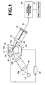
- a surface plasmon resonance sensor of this embodiment comprises a measuring chip 10 (a type of the sensor unit) , a laser 14 which may comprise, for instance, a semiconductor laser which emits a light beam L for measurement (a laser beam), a light beam projecting optical system 15 which causes the light beam L to impinge upon the measuring chip 10, a collimator lens 16, a photodetector 17, a signal processing system 20 which controls drive of the laser 14 and effects the process to be described later upon receipt of the output signal S of the photodetector 17, a display means 21 connected to the signal processing system 20.
- a measuring chip 10 a type of the sensor unit
- a laser 14 which may comprise, for instance, a semiconductor laser which emits a light beam L for measurement (a laser beam)
- a light beam projecting optical system 15 which causes the light beam L to impinge upon the measuring chip 10
- a collimator lens 16 which causes the light beam L to impinge upon the measuring chip 10
- a collimator lens 16 which causes the light
- the measuring chip 10 comprises a dielectric block 11 substantially of a rectangular pyramid, a metal film 12 (e.g., gold or silver) which is formed on one surface of the dielectric block 11, a sample holding frame 13 of a tubular member which defines a laterally closed space above the metal film 12.
- the sample holding frame 13 is circular in cross-section and the inner surface thereof flares upward.
- the flared space in the sample holding frame 13 functions as a well 13a in which sample liquid 5 is stored.
- the dielectric block 11 and the sample holding frame 13 are integrally molded by transparent resin having a refractive index to be described later.
- a sensing medium 14, which is combined with a particular material, is fixed on the metal film 12.
- the transparent resin forming the dielectric block 11 has a refractive index which satisfies the relation -2 ⁇ 10 -5 ⁇ (n3 ⁇ n1-n1 ⁇ n3) ⁇ 2 ⁇ 10 -5 wherein n1 and n3 represent refractive indexes of the solvent of the sample liquid 5 and the dielectric block 11, and ⁇ n1 and ⁇ n3 represent the rates of temperature-change dn1/dt and dn3/dt of the refractive indexes of the solvent of the sample liquid 5 and the dielectric block 11.
- the light beam projecting optical system 15 collects the light beam L and causes the light beam L to enter the dielectric block 11 in a collected state to impinge upon the interface 12a between the dielectric block 11 and the metal film 12 at various angles of incidence.
- the light beam projecting optical system 15 comprises a collimator lens 15a which converts the light beam L emitted from the laser 14 as a divergent light beam, into a parallel light, and a condenser lens 15b which condenses the collimated light beam L on the interface 12a.
- the angle of incidence of the light beam L to the interface 12a is in such a range that total internal reflection conditions are satisfied and surface plasmon resonance occurs at the interface 12a.
- the light beam L is caused to impinge upon the interface 12a in a p-polarized state. This can be realizedbypositioning the laser 14 so that its direction of polarization is directed in a predetermined direction. Otherwise, the direction of polarization of the light beam L may be controlled by a wavelength plate or a polarizing plate.
- the photodetector 17 comprises a line sensor formed of a plurality of photosensor elements which are arranged in a row extending in a direction of arrow X in Figure 1.
- the light beam L is converted into a parallel light beam by a collimator lens 16 after reflected in total internal reflection at the interface 12a, and then detected by the photodetector 17.
- the surface plasmon resonance sensor has a temperature-control means comprising a thermistor 50 which measures the temperature of the dielectric block 11, a Peltier element 52 which controls a temperature and a driver 51 which drives the Peltier element 52.
- the temperature-control may be effected in other various ways.
- the thermistor 50 is in contact with a side surface of the dielectric block 1 in this embodiment, the thermistor 50 may be located in any position so long as it can measure the temperature of the dielectric block 11 if a thermal equilibrium is established between the dielectric block 11 and the environment.
- the Peltier element 52 is located on the bottom of the bottom of the dielectric block 11, it need not be disposed there.
- the temperature-control means controls the temperature during measurement within about 0.01°C.
- the measuring chip 10 is supplied with the sample liquid 5.
- the laser 14 is driven under instruction of the signal processing system 20 and a light beam L is emitted from the laser 14 impinges upon the interface 12a between the dielectric block 11 and the metal film 12.
- the light beam L impinging upon the interface 12a is reflected in total internal reflection at the interface 12a and the reflected light beam L is detected by the photodetector 17.
- the light beam L emitted from the laser 14 as a divergent light beam is focused on the interface 12a. Accordingly, the light beam L includes components impinging upon the interface at various angles of incidence of the light beam L to the interface 12a and the reflected light beam L includes components reflected at the interface 12a at various angles of reflection.
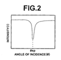
- the component of the light beam L impinging upon the interface 12a at a particular angle of incidence ⁇ sp excites surface plasmon in the interface 12a between the metal film 12 andmaterial in contact with the metal film 12 and the intensity of the component reflected in total internal reflection sharply drops. That is, the particular angle of incidence ⁇ sp is the attenuation angle or the angle at which the total internal reflection is cancelled and the intensity of the reflected light beam exhibits a minimum value at the angle of incidence ⁇ sp.
- the region where the intensity I of the reflected light beam sharply drops is generally observed as a dark line D in the reflected light beam L.
- Figure 2 is a view showing the relation between the angle of incidence ⁇ of the light beam L to the interface and the intensity I of the light beam received by the photodetector 17.
- the signal processing system 20 detects the amounts of light detected by the photosensor elements on the basis of the signal S output from the photodetector 17 and determines the attenuation angle ⁇ sp on the basis of the position of the photosensor element detecting the dark line.
- the light beam projecting optical system 15 may be arranged to cause the light beam L to impinge upon the interface 12a in a defocused state. In this way, errors in measurement of the state of surface plasmon resonance (e.g., measurement of the position of the dark line) are averaged and the measuring accuracy can be improved.
- the refractive index of the sensing medium 14 on the metal film 12 changes with change of the state of combination of the particular material with the sensing medium 14.
- change in the state of combination of the particular material with the sensing medium 14 can be investigated.
- the signal processing system 20 detects whether the particular material is in the sample liquid 5, and causes the display means 21 to display the result of detection.
- the temperature during measurement is controlled within about 0.01°C by the temperature-control means.
- the temperature-control means As described above, in the past, it has been impossible to obtain a reliability of 1RU in the measured value in measuring devices which accept a temperature fluctuation up to 0.01°C.
- fluctuation in the refractive index per 1°C can be suppressed to about 10RU, and accordingly, when temperature-control is conducted at an accuracy of 0.01°C, the fluctuation in the refractive index can be suppressed to about 1RU, and reliable high-sensitivity measurement up to 1RU can be realized.
- a combination of pure water or physiological saline (as the solvent) and Zeonex E48R (ZEON CORPORATION) (as the material of the dielectric block) can be, for instance, used.
- the absolute value of d ⁇ /dt constantly exceeds 10 when the dielectric block 11 is formed by a material other than Zeonex E48R, and accordingly, it is impossible to realize reliable high-sensitivity measurement up to 1RU even when temperature-control is conducted at an accuracy of 0.01°C.
- the values of the refractive index and the rates of temperature-change are given by data in catalogue from SCHOTT.
Landscapes
- Physics & Mathematics (AREA)
- Health & Medical Sciences (AREA)
- Life Sciences & Earth Sciences (AREA)
- Chemical & Material Sciences (AREA)
- Analytical Chemistry (AREA)
- Biochemistry (AREA)
- General Health & Medical Sciences (AREA)
- General Physics & Mathematics (AREA)
- Immunology (AREA)
- Pathology (AREA)
- Investigating Or Analysing Materials By Optical Means (AREA)
Applications Claiming Priority (2)
| Application Number | Priority Date | Filing Date | Title |
|---|---|---|---|
| JP2003331549A JP2005098788A (ja) | 2003-09-24 | 2003-09-24 | 表面プラズモン共鳴測定装置およびセンサユニット |
| JP2003331549 | 2003-09-24 |
Publications (1)
| Publication Number | Publication Date |
|---|---|
| EP1519187A1 true EP1519187A1 (fr) | 2005-03-30 |
Family
ID=34191451
Family Applications (1)
| Application Number | Title | Priority Date | Filing Date |
|---|---|---|---|
| EP20040022434 Withdrawn EP1519187A1 (fr) | 2003-09-24 | 2004-09-21 | Détecteur de résonance de plasmon et unité de détection pour mesurer exactement de petites fluctuations d'indice de réfraction |
Country Status (3)
| Country | Link |
|---|---|
| US (1) | US20050112028A1 (fr) |
| EP (1) | EP1519187A1 (fr) |
| JP (1) | JP2005098788A (fr) |
Cited By (1)
| Publication number | Priority date | Publication date | Assignee | Title |
|---|---|---|---|---|
| CN109884063A (zh) * | 2019-04-24 | 2019-06-14 | 金华伏安光电科技有限公司 | 一种用于液体传感器的采集结构 |
Families Citing this family (6)
| Publication number | Priority date | Publication date | Assignee | Title |
|---|---|---|---|---|
| JP2006349556A (ja) * | 2005-06-17 | 2006-12-28 | Fujikura Ltd | 表面プラズモンセンサ |
| EP1999455A2 (fr) * | 2006-03-10 | 2008-12-10 | Corning Incorporated | Microplaques de reference et procedes de fabrication et d'utilisation associes |
| RU2497100C2 (ru) * | 2007-10-29 | 2013-10-27 | Конинклейке Филипс Электроникс Н.В. | Контейнер биодатчика с нарушенным полным внутренним отражением |
| WO2013027544A1 (fr) * | 2011-08-25 | 2013-02-28 | コニカミノルタホールディングス株式会社 | Dispositif de mesure et puce de détection |
| GB201721611D0 (en) * | 2017-12-21 | 2018-02-07 | Univ College Dublin Nat Univ Ireland Dublin | Addressable plasmonic arrays |
| JP7369381B2 (ja) * | 2019-12-16 | 2023-10-26 | 東芝テック株式会社 | 検出装置 |
Citations (3)
| Publication number | Priority date | Publication date | Assignee | Title |
|---|---|---|---|---|
| EP1186881A1 (fr) * | 2000-03-16 | 2002-03-13 | Fuji Photo Film Co., Ltd. | Procede et instrument de mesure utilisant l'attenuation de la reflexion totale |
| US20030062842A1 (en) * | 2001-09-28 | 2003-04-03 | Yoshimitsu Nomura | Measuring chip and method of manufacture thereof |
| US20030090668A1 (en) * | 2001-11-12 | 2003-05-15 | Fuji Photo Film Co., Ltd. | Measuring method and apparatus using attenuation in total internal reflection |
Family Cites Families (7)
| Publication number | Priority date | Publication date | Assignee | Title |
|---|---|---|---|---|
| GB2197065A (en) * | 1986-11-03 | 1988-05-11 | Stc Plc | Optical sensor device |
| US4990559A (en) * | 1989-02-14 | 1991-02-05 | Mitsui Petrochemical Industries, Ltd. | Thermoplastic resin composition |
| GB9111912D0 (en) * | 1991-06-04 | 1991-07-24 | Fisons Plc | Analytical methods |
| WO1997015821A1 (fr) * | 1995-10-25 | 1997-05-01 | University Of Washington | Sondes de detection a resonance de plasmon de surface a conducteur de lumiere plan coude |
| US6646744B2 (en) * | 2000-07-21 | 2003-11-11 | Vir A/S | Coupling elements for surface plasmon resonance sensors |
| KR100407821B1 (ko) * | 2001-11-23 | 2003-12-01 | 한국전자통신연구원 | 활성이온의 상향전이를 이용한 도파로-플라즈몬 공명 센서및 이미징 시스템 |
| US6985664B2 (en) * | 2003-08-01 | 2006-01-10 | Corning Incorporated | Substrate index modification for increasing the sensitivity of grating-coupled waveguides |
-
2003
- 2003-09-24 JP JP2003331549A patent/JP2005098788A/ja active Pending
-
2004
- 2004-09-21 EP EP20040022434 patent/EP1519187A1/fr not_active Withdrawn
- 2004-09-23 US US10/947,285 patent/US20050112028A1/en not_active Abandoned
Patent Citations (3)
| Publication number | Priority date | Publication date | Assignee | Title |
|---|---|---|---|---|
| EP1186881A1 (fr) * | 2000-03-16 | 2002-03-13 | Fuji Photo Film Co., Ltd. | Procede et instrument de mesure utilisant l'attenuation de la reflexion totale |
| US20030062842A1 (en) * | 2001-09-28 | 2003-04-03 | Yoshimitsu Nomura | Measuring chip and method of manufacture thereof |
| US20030090668A1 (en) * | 2001-11-12 | 2003-05-15 | Fuji Photo Film Co., Ltd. | Measuring method and apparatus using attenuation in total internal reflection |
Non-Patent Citations (4)
| Title |
|---|
| "Zeonex. Basic properties", ZEON CORPORATION . SPECIALTY PLASTICS PRODUCT INFORMATION, 20 August 2003 (2003-08-20), XP002309554, Retrieved from the Internet <URL:http://web.archive.org/web/20030820181254/http://www.zeon.co.jp/business_e/enterprise/speplast/speplast1_8.html> [retrieved on 20041207] * |
| "Zeonex. Precise optical properties", ZEON CORPORATION . SPECIALTY PLASTICS PRODUCT INFORMATION, 20 August 2003 (2003-08-20), XP002309555, Retrieved from the Internet <URL:http://web.archive.org/web/20030820182333/http://www.zeon.co.jp/business_e/enterprise/speplast/speplast1_7.html> [retrieved on 20041207] * |
| NATSUUME T ET AL: "A NEW HIGH HEAT RESISTANT, HIGH CLARITY, AND HIGH HUMIDITY RESISTANT POLYMER FOR OPTICAL USES", MATERIALS RESEARCH SOCIETY SYMPOSIUM PROCEEDINGS, MATERIALS RESEARCH SOCIETY, PITTSBURG, PA, US, vol. 150, 25 April 1989 (1989-04-25), pages 245 - 250, XP009007850, ISSN: 0272-9172 * |
| SULTANOVA N G ET AL: "Measuring the refractometric characteristics of optical plastics", OPTICAL AND QUANTUM ELECTRONICS KLUWER ACADEMIC PUBLISHERS NETHERLANDS, vol. 35, no. 1, January 2003 (2003-01-01), pages 21 - 34, XP002309553, ISSN: 0306-8919 * |
Cited By (2)
| Publication number | Priority date | Publication date | Assignee | Title |
|---|---|---|---|---|
| CN109884063A (zh) * | 2019-04-24 | 2019-06-14 | 金华伏安光电科技有限公司 | 一种用于液体传感器的采集结构 |
| CN109884063B (zh) * | 2019-04-24 | 2021-08-20 | 杭州翔毅科技有限公司 | 一种用于液体传感器的采集结构 |
Also Published As
| Publication number | Publication date |
|---|---|
| JP2005098788A (ja) | 2005-04-14 |
| US20050112028A1 (en) | 2005-05-26 |
Similar Documents
| Publication | Publication Date | Title |
|---|---|---|
| EP1079225A1 (fr) | Capteur de plasmons de surface pour l'analyse d'un échantillon liquide ou d'une atmosphère humide | |
| US8705033B2 (en) | Multi-channel surface plasmon resonance sensor using beam profile ellipsometry | |
| US6791691B2 (en) | Measuring method and apparatus using attenuation in total internal reflection | |
| US7064837B2 (en) | Measuring sensor utilizing attenuated total reflection and measuring chip assembly | |
| US6885454B2 (en) | Measuring apparatus | |
| EP1324019B1 (fr) | Capteur utilisant ondes évanescentes | |
| US7144153B2 (en) | Measuring apparatus | |
| EP1308714B1 (fr) | Plaque de mesure pour capteur utilisant la réflexion totale atténuée | |
| US7057731B2 (en) | Measuring method and apparatus using attenuated total reflection | |
| EP1519187A1 (fr) | Détecteur de résonance de plasmon et unité de détection pour mesurer exactement de petites fluctuations d'indice de réfraction | |
| US7009706B2 (en) | Measuring chip | |
| US7330263B2 (en) | Measurement method and apparatus | |
| US6788415B2 (en) | Turntable measuring apparatus utilizing attenuated total reflection | |
| US20020154312A1 (en) | Measuring apparatus utilizing attenuated total reflection | |
| US7075657B2 (en) | Surface plasmon resonance measuring apparatus | |
| JP3910498B2 (ja) | 測定装置 | |
| JP2002195942A (ja) | 全反射減衰を利用したセンサー | |
| JP2002296176A (ja) | 全反射減衰を利用したセンサー | |
| JP3776371B2 (ja) | 測定装置 | |
| JP2003139693A (ja) | 全反射減衰を利用した測定方法および測定装置 | |
| JP2003139692A (ja) | 全反射減衰を利用したセンサー | |
| JP2002195943A (ja) | 全反射減衰を利用したセンサー | |
| JP2002207006A (ja) | 全反射減衰を利用したセンサー | |
| JP2004125494A (ja) | 測定装置 | |
| JP2003185571A (ja) | 全反射減衰を利用したセンサー |
Legal Events
| Date | Code | Title | Description |
|---|---|---|---|
| PUAI | Public reference made under article 153(3) epc to a published international application that has entered the european phase |
Free format text: ORIGINAL CODE: 0009012 |
|
| AK | Designated contracting states |
Kind code of ref document: A1 Designated state(s): AT BE BG CH CY CZ DE DK EE ES FI FR GB GR HU IE IT LI LU MC NL PL PT RO SE SI SK TR |
|
| AX | Request for extension of the european patent |
Extension state: AL HR LT LV MK |
|
| 17P | Request for examination filed |
Effective date: 20050603 |
|
| AKX | Designation fees paid |
Designated state(s): CH DE FR GB LI SE |
|
| RAP1 | Party data changed (applicant data changed or rights of an application transferred) |
Owner name: FUJIFILM CORPORATION |
|
| 17Q | First examination report despatched |
Effective date: 20080205 |
|
| STAA | Information on the status of an ep patent application or granted ep patent |
Free format text: STATUS: THE APPLICATION IS DEEMED TO BE WITHDRAWN |
|
| 18D | Application deemed to be withdrawn |
Effective date: 20080617 |