RELATED APPLICATIONS
This application is related to the application assigned attorney
docket number EL-0495, United States Application Serial Number
60/418045, filed in the United States Patent and Trademark Office on
October 11, 2002, and entitled "CO-FIRED CERAMIC CAPACITORS AND
METHOD FOR FORMING CERAMIC CAPACITORS FOR USE IN
PRINTED WIRING BOARDS," the application assigned attorney docket
number EL-0496, United States Application Serial Number 60/433105,
filed on December 13, 2002, and entitled "PRINTED WIRING BOARDS
HAVING LOW INDUCTANCE EMBEDDED CAPACITORS AND
METHODS OF MAKING SAME," and the application assigned attorney
docket number EL-0497, United States Application Serial Number
60/453129, filed on March 7, 2003 and entitled "PRINTED WIRING
BOARDS HAVING CAPACITORS AND METHODS OF MAKING
THEREOF."
BACKGROUND
TECHNICAL FIELD
The technical field is capacitors. More particularly, the technical
field includes high tolerance value capacitors that may be embedded in
printed wiring boards.
BACKGROUND ART
The practice of embedding passive circuit elements in printed wiring
boards (PWB) allows for reduced circuit size and improved circuit
performance. Passive circuit elements are typically embedded in panels
that are stacked and connected by interconnection circuitry, with the stack
of panels forming the printed wiring board. The panels can be generally
referred to as "innerlayer panels."
Capacitors have varying requirements depending upon their
intended uses. In many circuits, capacitor tolerance, which is the
allowable variation around a target capacitance value, is critical. For
example, in timing and analog-to-digital (A/D) conversion applications,
capacitors generally have low capacitance values and high tolerances.
Some of these capacitors have tolerance requirements of less than +/- 5%
variation around their target value. In such cases, the high tolerance
requirement is not easily obtained by common embedding techniques,
such as screen printing or etching. Such capacitors may therefore be
unsuitable for many applications requiring high tolerance.
The following US patent illustrates the state of the prior art.
U.S, 4,190,854 to Redfern, discloses a capacitor suitable for
integration into a monolithic integrated circuit which is fabricated in two
parallel connected sections. One section, using a thin oxide, constitutes
most of the capacitance. A second section which is fabricated on a thick
oxide constitutes a smaller capacitance per unit area but can be laser
trimmed to provide a precise capacitance without damage to the
integrated circuit. The trimmable section is desirably made using a
conductive electrode material that is readily removed with laser energy.
SUMMARY
According to a first embodiment, a printed wiring board is
constructed from innerlayer panels. A capacitor in an innerlayer panel is
made by forming a first electrode layer comprising a plurality of electrode
portions, forming a dielectric contacting the first electrode layer, and
forming a second electrode layer spaced from the first electrode layer,
wherein the first electrode layer, the dielectric and the second electrode
layer form a first capacitor. The capacitance of the capacitor may be set
to have a capacitance that exceeds a desired or target capacitance value.
One or more of the electrode portions of the first electrode layer are then
trimmed or cut by a laser in order to disconnect a section of electrode from
the capacitor so that the capacitance is lowered to a value that is close to
or at the target value. The capacitor may be encased in organic dielectric
material and incorporated into the printed wiring board along with
additional innerlayer panels.
According to a second embodiment, a capacitor comprises a first
electrode layer comprising a first plurality of elongated electrode portions,
a second electrode layer comprising a second plurality of electrode
portions spaced from and interdigitated with the first plurality of electrode
portions, and a dielectric disposed between the first and second pluralities
of electrode portions. One or more of the electrode portions may be
trimmed in order to bring the capacitor to a target capacitance value.
Those skilled in the art will appreciate the above stated advantages
and other advantages and benefits of various embodiments of the
invention upon reading the following detailed description of the
embodiments with reference to the below-listed drawings.
According to common practice, the various features of the drawings
are not necessarily drawn to scale. Dimensions of various features may
be expanded or reduced to more clearly illustrate the embodiments of the
invention.
BRIEF DESCRIPTION OF THE DRAWINGS
The detailed description will refer to the following drawings, wherein
like numerals refer to like elements, and wherein:
DETAILED DESCRIPTION
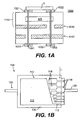
FIG. 1A is a schematic section view in front elevation of a printed
wiring board 1000 according to a first embodiment of the invention. The
printed wiring board 1000 comprises an innerlayer panel 1100 having an
embedded capacitor 105. One innerlayer panel 1100 is illustrated in FIG.
1A. The printed wiring board 1000 can, however, comprise two or more
innerlayer panels. According to the first embodiment, the capacitor 105
has trimmable electrodes.
Referring to FIG. 1A, the capacitor 105 is electrically coupled to two
circuit conductors 1001, 1002 extending through the printed wiring board
1000. The completed innerlayer panel 1100, before incorporation in the
printed wiring board 1000, is illustrated in FIG. 1I.
Referring to FIG. 1A, the printed wiring board 1000 includes
connection circuitry 1021, 1022 and 1031, 1032 at opposite ends of the
board 1000. The printed wiring board 1000 may also include a power
plane 1010 and a ground plane 1012. The power plane 1010 may be
formed as part of the innerlayer panel 1100. An exemplary device D is
shown as coupled to the connection circuitry 1021, 1022. The device D
can be, for example, a semiconductor chip.
FIG. 1B is a top plan view of the capacitor 105 schematically
illustrated in FIG. 1A. The capacitor 105 includes a first electrode layer
110, a second electrode layer 120, and a dielectric 130. The first
electrode layer 110 is separated from the second electrode layer 120 by
the dielectric 130. Only a portion of the second electrode layer 120 is
shown in FIG. 1B. The first electrode layer 110 may be electrically
isolated from the second electrode layer 120 by a trench (not shown in
FIG. 1B). The second electrode layer 120 can be formed from, for
example, a metallic foil.
Referring to FIG. 1B, the first electrode layer 110 includes a
plurality of electrode portions 114 of varying size, and a main electrode
112. The electrode portions 114 are connected to a conductive portion
126 by conductive portions 116. The main electrode 112 is electrically
connected to the conductive portion 126 by a conductive portion 113. The
first electrode layer 110 can be selectively trimmed across the conductive
portions 116 in order to control the capacitance provided by the capacitor
105. A trim direction is indicated as the arrow T in FIG. 1B, and the
trimming operation is discussed in detail below with reference to FIG. 1F.
The main electrode 112 may be much larger than the electrode portions
114. Inclusion of the smaller trimmable electrode portions 114 allows for
fine control of the total capacitance of the capacitor 105.
A method of making the innerlayer panel 1100 and a method of
incorporating the innerlayer panel 1100 into the printed wiring board 1000
are discussed in detail below with reference to FIGS. 1C-1I. The
completed innerlayer panel 1100, before incorporation into the printed
wiring board 1000, is illustrated in FIG. 1I. The innerlayer panel
embodiment discussed below is a polymeric capacitor embodiment. Other
materials of construction, however, may be used to form the innerlayer
panel 1100.
FIG. 1C is a section view in front elevation of a first stage of
manufacture of the innerlayer panel 1100. In FIG. 1C, a metallic foil 10 is
provided. The foil 10 may be of a type generally available in the industry.
For example, the foil 10 may be copper, copper-invar-copper, invar, nickel,
nickel-coated copper, or other metals. Preferred foils include foils
comprised predominantly of copper, such as reverse-treated copper foils,
double-treated copper foils, and other copper foils commonly used in the
multilayer printed circuit board industry.
The thickness of the foil 10 may be in the range of, for example,
about 1-100 microns, preferably 3-75 microns, and most preferably 12-36
microns, corresponding to between about 1/3 oz and 1 oz copper foil. The
foil 10 is laminated to a first laminate material 160. The laminate material
160 may be, for example, FR4 prepreg and/or other organic materials.
FIG. 1D is a top plan view of the next stage of manufacture, and
FIG. 1E is a section view taken on line 1E-1E in FIG. 1D. Referring to
FIG. 1E, a photo-resist is applied to the foil 10 (reference number 10 is not
used in FIGS. 1D and 1E), and the foil 10 is imaged, etched and stripped
using, for example, standard printing wiring board processing conditions.
Etching the foil 10 results in the second electrode layer 120 and the
conductive portion 126 shown in FIG. 1D. A trench 122 isolates the
second electrode layer 120 from the conductive portion 126.
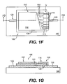
FIG. 1F is a top plan view of a next stage of manufacture, and FIG.
1G is a section view taken on line 1G-1G in FIG. 1F. Referring to FIGS.
1F and 1G, the dielectric 130 is formed over the second electrode layer
120. The dielectric 130 fills the trench 122. The dielectric 130 may be
formed from, for example, a polymer thick film (PTF) paste, and may be
applied by, for example, solution casting or screen printing. The dielectric
130 is then cured. Solvents present in the dielectric 130 are removed
during the curing process.
A first electrode layer 110 is then formed over the dielectric 130,
forming the electrode portions 114, the main electrode 112 and the
conductive portions 113, 116. The first electrode layer 110 may be formed
from, for example, a conductive PTF paste. The first electrode layer 110
is then cured.
At this stage, the capacitance of the resulting article is higher than
the capacitance that is ultimately desired for the finished capacitor. To
reduce the capacitance value to the desired or "target" value, one or more
of the electrode portions 114 may be selectively removed or disconnected
from the capacitor by trimming (or "cutting") one or more of the conductive
portions 116. In FIG. 1F, a trimming direction is indicated by an arrow T.
A UV-YAG laser is one preferred device to perform trimming. The UV-YAG
laser selectively cuts one or more conductive portions 116 to reduce
the total area of the electrode layer 110, thereby reducing the capacitance
of the capacitor 105. The electrode portions 114 can have successively
smaller sizes to provide flexibility in adjusting the capacitance of the
capacitor 105. The laser may be programmed with the electrode design
and use a feedback process in which the laser initially measures total
capacitance and calculates the number of electrode portions that are
required to be trimmed in order to avoid either undershooting or
overshooting the desired value. The laser may also measure the
capacitance change throughout the trimming process and may be
programmed to stop trimming within a certain range of the desired value.
High tolerance values can be achieved by selective trimming of the
electrode portions 114.
Referring to FIG. 1H, the resulting article is then laminated to a
second laminate material 170. A foil 180 is applied to the first laminate
material 160, and a foil 190 is applied to the second laminate material 170.
FIG. 1I illustrates the finished innerlayer panel 1100. Referring to
FIGS. 1H and 1I, the foil 180 is imaged, etched and stripped to form an
etched portion 1010. The etched portion 1010 can be, for example, a
power plane. The foil 190 is also imaged, etched and stripped to form the
connection circuitry 1021, 1022. After incorporating the innerlayer panel
1100 into the printed wiring board 1000, the circuit conductors 1001, 1002
can be formed through the printed wiring board 1000. A section of each of
the circuit conductors 1001, 1002 is shown in FIG. 1I.
Referring back to FIG. 1A, the innerlayer panel 1100 can be
stacked with other layers, including, for example, additional innerlayer
panels. The printed wiring board 1000 can be formed from multiple
stacked innerlayer panels by, for example, lamination processes. Stacked
innerlayer panels can be laminated together in one or more conventional
lamination pressings and bonded together using, for example, dielectric
prepregs. The printed wiring board 1000 may be laminated in multiple
stages. For example, subassemblies of innerlayer panels may be
processed and laminated, and one or more subassemblies can
subsequently be stacked and laminated together to form the finished
printed wiring board 1000.
Each of the innerlayer panels in the printed wiring board 1000 can
have a different design, including differing arrangements of circuit
elements. The term "innerlayer panel" does not imply that a panel must be
sandwiched in the interior of the printed wiring board 1000, and an
innerlayer panel can also be located on, for example, outside layers of the
printed wiring board 1000.
The first and second circuit conductors 1001, 1002 can be formed
as conductive vias, for example, by laser or mechanical drilling through the
printed wiring board 1100. The holes formed by drilling are then plated
with a conductive material. The resulting conductive vias 1001, 1002,
which extend through the entire printed wiring board 1000 shown in FIG.
1A, are typically referred to as "plated through-holes." Plated through-hole
type vias are usually formed after all of the innerlayer panels of a printed
wiring board have been laminated together. Additional circuit conductors
(not shown) in other parts of the printed wiring board 1000 could extend
through subassemblies of innerlayer panels or through individual
innerlayer panels. Via circuit conductors extending through only a part of
the printed wiring board 1000 are commonly referred to as "buried vias."
Buried vias are typically drilled and plated through a subassembly of
innerlayer panels before the subassembly of innerlayer panels is
incorporated into a printed wiring board. A small diameter conductive via
formed on one or both sides of an innerlayer panel is commonly referred
to as a "microvia," and may be used, for example, to terminate a capacitor
within an innerlayer panel. Any of the above-mentioned types of vias may
be connected to the innerlayer panel embodiments discussed in this
specification.
After all interconnections have been formed and all subassemblies
of innerlayer panels or individual innerlayer panels have been laminated
together, the printed wiring board 1000 is complete. In FIG. 1A, the
printed wiring board 1000 is illustrated as comprising the innerlayer panel
1100, the ground plane 1012, the power plane 1010 and additional
laminate layers in a stacked configuration. Any number of innerlayer
panels may be included in a printed wiring board according to the
embodiments discussed in this specification.
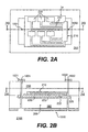
FIG. 2A is a top plan section view of a portion of an alternative
innerlayer panel 2100, taken on line 2A-2A in FIG. 2B. FIG. 2B is a
section view in front elevation, taken on line 2B-2B in FIG. 2A. The
innerlayer panel 2100 can be incorporated into a printed wiring board such
as, for example, the printed wiring board 1000 illustrated in FIG. 1A. FIG.
2B illustrates the innerlayer panel 2100 after its incorporation into the
printed wiring board 1000. The innerlayer panel 2100 includes a capacitor
205 laminated between layers 250 and 260 of laminate material.
The capacitor 205 includes a first electrode layer 210 comprised of
a plurality of electrode portions 215. The electrode portions 215 are
interconnected by a plurality of conductive portions 217. A dielectric 230
separates the second electrode layer 220 from the first electrode layer
210. The first electrode layer 210, including the electrode portions 215
and the conductive portions 217, is electrically connected to a conductive
portion 226. A trench 222 isolates the second electrode layer 220 from
the first electrode layer 210.
The first electrode layer 210, including the plurality of conductors
215, is electrically coupled to the second circuit conductor 1002. The
second electrode layer 220 is electrically coupled to the first circuit
conductor 1001. In FIG. 2B, the circuit conductor sections 1001, 1002
correspond to a portion of the circuit conductors 1001, 1002 illustrated in
FIG. 1A.
The capacitance of the capacitor 205 can be varied to within small
variances by trimming one or more of the electrode portions 215. The
trimming is performed on innerlayer panel 2100 by trimming through the
laminate 250 and through the conductive portions 217. Circuit conductors
1021, 1022 may serve as probe points, for example, for testing the
capacitance of the capacitor 205. The electrode portions 215 can be
trimmed in a variety of combinations and locations, allowing for fine control
of the capacitance provided by the capacitor 205. The process for making
the innerlayer panel 2100, including the trimming process, is described
below with reference to FIGS. 2C-2J.
The embodiment discussed below is a fired-on-foil embodiment
using co-firing of capacitor layers. Other methods of construction,
however, may be used to form the innerlayer panel 2100.
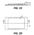
FIG. 2C is a section view in front elevation of a first stage of
manufacturing the innerlayer panel 2100. In FIG. 2C, a metallic foil 40 is
provided. The foil 40 may be of a type generally available in the industry.
For example, the foil 40 may be copper, copper-invar-copper, invar, nickel,
nickel-coated copper, or other metals that have melting points in excess of
the firing temperature for thick-film pastes.
The foil 40 may be pretreated, for example, by applying and firing
an underprint 42. The underprint 42 is a relatively thin layer applied to a
component-side surface of the foil 40. In FIG. 2C, the underprint 42 is
indicated as a surface coating on the foil 40. The underprint 42 adheres
well to the metal foil 40 and to layers deposited over the underprint 42.
The underprint 42 may be formed, for example, from a paste applied to the
foil 40, which is then fired at a temperature below the melting point of the
foil 40. The paste may be printed as an open coating over the entire
surface of the foil 40, or printed on selected areas of the foil 40.
A dielectric material is screen-printed over the underprint 42,
forming a first dielectric layer 51. The dielectric material may be, for
example, a thick-film dielectric ink. The dielectric ink may be formed of, for
example, a paste. The first dielectric layer 51 is then dried. A second
dielectric layer 52 is then applied and dried. In an alternative embodiment,
a single layer of dielectric material may be deposited through a mesh
screen that is coarser than the mesh screen used to form the two separate
layers 51, 52. The coarser mesh screen provides an equivalent thickness
in one printing step.
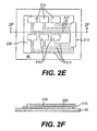
Referring to FIGS. 2E and 2F, a first electrode layer 210 is formed
over the second dielectric layer 52 ( reference numbers 51 and 52 are not
used in FIGS. 2E and 2F) and dried. The first electrode layer 210 may be
formed by, for example, screen-printing a thick-film metallic ink. The first
electrode layer 210 is comprised of the plurality of electrode portions 215,
which are interconnected by the plurality of conductive portions 217. A
portion of the first electrode layer 210 extends over the dielectric layer 52
and contacts the foil 40. In general, the surface area of the dielectric
layer 52, when viewed from a top plan perspective, should be larger than
that of the first electrode layer 210.
The first dielectric layer 51, the second dielectric layer 52, and the
first electrode layer 210 are then co-fired. "Co-fired" means that the layers
51, 52 are not fired prior to forming the first electrode layer 210. The post-fired
structure is shown in FIGS. 2E and 2F. A dielectric 230 results from
the co-firing step. The thick-film dielectric layers 51, 52 may be formed of,
for example, a high K functional phase such as, for example, barium
titanate and a dielectric property-modifying additive such as, for example,
zirconium dioxide, mixed with a glass-ceramic frit phase. During co-firing,
the glass-ceramic frit phase softens, wets the functional and additive
phases and coalesces to create a dispersion of the functional phase and
the modifying additive in a glass-ceramic matrix. At the same time, the
first electrode layer 210 and the foil 40 are wetted by the softened glass-ceramic
frit phase and sintered together. The first electrode layer 210 and
the foil 40 have a strong bond to the high K dielectric 230 that results from
the co-firing.
Referring to FIG. 2G, the structure is laminated on a first side of the
foil 40 (reference number 40 is not used in FIG. 2G). For example, the
component-side face of the foil 40 can be laminated to a laminate material
250 and to a conductive foil 252. The lamination can be performed, for
example, using FR4 prepreg or other organic materials in standard printing
wiring board processes.
After lamination, a photo-resist is applied to the foil 40 and the foil
40 is imaged, etched and stripped using, for example, standard printing
wiring board processing conditions. The second electrode layer 220
results from the etching of the foil 40. The etching creates a trench 222 in
the foil 40 which breaks electrical contact of the first electrode layer 210
from the second electrode layer 220. A portion 226 of the foil 40 is
electrically connected to the first electrode layer 210. The electrode layers
210 and 220 and the dielectric 230 form the capacitor 205. The foil 252
may be etched at this time or at a later time. The foil 252 may be etched
to form the circuitry 1021, 1022 illustrated in FIG. 2B.
Referring to FIG. 2H, the resulting article is laminated on a second
side of the second electrode layer 220 to a second laminate material 260.
A foil 262 may be applied to the second laminate material 260. The foil
262 may be etched to form circuitry. The foil 262 can be etched, for
example, to form the power plane 1010 illustrated in FIG. 2B. Foil 252
may also be etched at this time.
According to this embodiment, the first electrode layer 210 may
now be selectively trimmed in order to control the capacitance provided by
the capacitor 205 (the capacitor 205 is shown in FIGS. 2A and 2B).
Methods and patterns of trimming the first electrode layer 210 are
discussed in detail below with reference to FIGS. 2I and 2J.
FIG. 2H illustrates the innerlayer panel 2100 before integration of
the innerlayer panel 2100 into the printed wiring board 1000 illustrated in
FIG. 1A, and before formation of the circuitry 1021, 1022, 1001, 1002 and
the power plane 1010. FIGS. 2A and 2B illustrate the innerlayer panel
2100 after its incorporation into the printed wiring board 1000. The printed
wiring board 1000 can be formed from multiple stacked innerlayer panels
by, for example, lamination processes. The innerlayer panels can be
laminated together in one or more lamination pressings. The innerlayer
panels can be bonded together using, for example, dielectric prepregs and
other organic materials, and may be laminated in multiple stages.
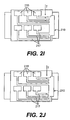
FIGS. 2I and 2J illustrate two exemplary trimming operations for the
electrode 210. According to this embodiment, the electrode layer 210 may
be selectively trimmed in order to control the capacitance provided by the
capacitor 205 (FIGS. 2A and 2B). Trimming may be performed using, for
example, a UV-YAG laser or a CO2 laser or a combination of both.
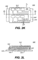
FIGS. 2K and 2L illustrate an alternative embodiment to the
capacitor 205 illustrated in FIGS. 2A and 2B. FIG. 2K is a top plan view of
a capacitor 205', and FIG. 2L is a section view in front elevation taken on
line 2L-2L in FIG. 2K. The capacitor 205' includes a first electrode layer
210', a second electrode layer 220', a third electrode layer 230', and a
dielectric 240'. The first and third electrode layers 210', 230' are
separated from the second electrode layer 220' by the two-layer dielectric
240'. The first and third electrode layers 210', 230' are electrically isolated
from the second electrode layer 220' by a trench 232'. The third electrode
layer 230' can be formed from, for example, a metallic foil.
Referring to FIG. 2K, the first electrode layer 210' includes a
plurality of electrode portions 215' which are electrically coupled by
conductive portions 217'. The first electrode layer 210' can be selectively
trimmed in order to control the capacitance provided by the capacitor 205',
as discussed above with reference to FIGS. 2I and 2J. The three-electrode,
two-layer dielectric structure of the capacitor 205' provides a
high capacitance.
The capacitor 205' can be formed in a manner similar to the
capacitor 205 (FIGS. 2A and 2B), and can be similarly laminated and
incorporated in a printed wiring board. When forming the capacitor 205',
however, additional layers of dielectric are formed over the second
electrode layer 220', and the first electrode layer 210' is formed over the
additional dielectric layers. The capacitor 205' may be fired in one or in
multiple firings. For example, the article can be fired after forming the
second electrode layer 220', and fired again after forming the first
electrode layer 210'. Alternatively, a single co-firing can be performed
after forming the first electrode layer 210'. A single co-firing is
advantageous in that production costs are reduced. Two separate firings,
however, allow for inspection of the second electrode layer 220' for
defects, such as printing alignment problems, after the first firing.
The first and third electrode layers 210', 230' may be electrically
connected to a circuit conductor (not shown) contacting the third electrode
layer 230'. The second electrode layer 220' can be electrically connected
to a circuit conductor (not shown) contacting a conductive portion 236'.
The circuit conductors connecting to the capacitor 205' can be similar to
the circuit conductors 1001, 1002 illustrated in FIG. 1A. Other circuit
conductor configurations are also possible.
FIGS. 3A and 3B illustrate yet another alternative embodiment of a
capacitor. FIG. 3A is a top plan view of a capacitor 305, and FIG. 3B is a
section view in front elevation taken on line 3B-3B in FIG. 3A. The
capacitor 305 includes a first electrode layer 310, a second electrode layer
320, and a dielectric 330. The capacitor 305 is formed over an organic
laminate material 350. The first electrode layer 310 is separated from the
second electrode layer 320 by the dielectric 330. The first electrode layer
310 may be electrically isolated from the second electrode layer 320 by a
trench 322. The second electrode layer 320 can be formed from, for
example, a metallic foil.
Referring to FIG. 3A, the first electrode layer 310 includes a
plurality of elongated electrode portions 315. The electrode portions 315
can be selectively trimmed in order to control the capacitance provided by
the capacitor 305, as discussed above with reference to FIGS. 1J and 1K.
The capacitor 305 can be formed in a manner similar to the
capacitor 105 illustrated in FIG. 1B, using polymer thick film dielectric and
conductor pastes. The capacitor 305 can be laminated and incorporated
in a printed wiring board.
The first electrode layer 310 may be electrically connected to a
circuit conductor (not shown) contacting a conductive portion 326. The
second electrode layer 320 can be electrically connected to a circuit
conductor (not shown) contacting the second electrode layer 320. The
circuit conductors connecting to the capacitor 305 can be similar to the
circuit conductors 1001, 1002 illustrated in FIG. 1A.
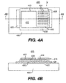
FIGS. 4A and 4B illustrate yet another alternative embodiment of a
capacitor. FIG. 4A is a top plan view of a capacitor 405, and FIG. 4B is a
section view in front elevation taken on line 4B-4B in FIG. 4A. The
capacitor 405 includes a first electrode layer 410, a second electrode layer
420, and a dielectric 430. The capacitor 405 is formed over a laminate
material 450. The first electrode layer 410 is separated from the second
electrode layer 420 by the dielectric 430. The first electrode layer 410
may be electrically isolated from the second electrode layer 420 by a
trench 422. The second electrode layer 420 can be formed from, for
example, a metallic foil.
Referring to FIG. 4A, the first electrode layer 410 includes a
plurality of electrode portions 414. The first electrode layer 410 can be
selectively trimmed across the electrode portions 414 in order to control
the capacitance provided by the capacitor 405. The first electrode layer
410 also includes a main electrode 412. Inclusion of the electrode
portions 414 allows for fine control of the capacitance of the capacitor 405
because a relatively small portion of the first electrode layer 410
selectively trimmed.
The capacitor 405 can be formed in a manner similar to the
capacitor 105 illustrated in FIG. 1B, using polymer thick film dielectric and
conductor pastes. The capacitor 405 can be laminated and incorporated
in a printed wiring board.
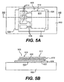
FIGS. 5A and 5B illustrate yet another alternative embodiment of a
capacitor. FIG. 5A is a top plan view of a capacitor 505, and FIG. 5B is a
section view in front elevation taken on line 5B-5B in FIG. 5A. The
capacitor 505 includes a first electrode layer 510, a second electrode layer
520, and a dielectric 530. The capacitor 505 is formed over a laminate
material 550. The first electrode layer 510 is separated from the second
electrode layer 520 by the dielectric 530. The first electrode layer 510
may be electrically isolated from the second electrode layer 520 by a
trench 522. The second electrode layer 520 can be formed from, for
example, a metallic foil.
Referring to FIG. 5A, the first electrode layer 510 includes a
plurality of electrode portions 514. The first electrode layer 510 can be
selectively trimmed across conductive portions 516 in order to control the
capacitance provided by the capacitor 505. The first electrode layer 510
also includes a main electrode 512 connected to the electrode portions
514 by the conductive portions 516. The main electrode 512 may be
much larger than the electrode portions 514. Inclusion of the trimmable
electrode portions 514 allows for fine control of the capacitance of the
capacitor 505.
FIGS. 6A-6C illustrate yet another embodiment of a capacitor. In
FIGS. 6A-6C, a capacitor 605 is embedded in an innerlayer panel 6100.
FIG. 6A is a section view taken on line 6A-6A in FIG. 6C, and FIG. 6B is a
section view taken on line 6B-6B in FIG. 6C. FIG. 6C is a section view
taken on line 6C-6C in FIG. 6A
Referring to FIGS. 6A and 6C, the innerlayer panel 6100 comprises
the capacitor 605 laminated to laminate materials 660, 670. The
innerlayer panel 6100 is illustrated as it would appear after incorporation
into a printed wiring board, such as the printed wiring board 1000
illustrated in FIG. 1A.
The capacitor 605 comprises a first electrode layer 610, a second
electrode layer 620, and a dielectric 630. A trench 622 electrically isolates
the first electrode layer 610 from the second electrode layer 620.
Referring to FIG. 6A, the first electrode layer 610 comprises a plurality of
elongated electrode portions 615. The capacitance value of the capacitor
605 is above the desired capacitance. The first electrode layer 610 can be
selectively trimmed at the elongated electrode portions 615 in order to
reduce the capacitance of the capacitor 605 to the desired value.
Referring to FIGS. 6A and 6C, an electrode portion 615 can be
trimmed without damaging the second electrode layer 620. Specifically,
when one or more electrode portions 615 are trimmed at the location
indicated by the arrow T, if the trimming laser beam passes through the
dielectric 630, the laser beam will not damage the second electrode layer
620 because the second electrode layer 620 does not extend over that
part of the dielectric 630. A method of making the innerlayer panel 6100 is
illustrated in FIGS. 6D-6F.
Referring to FIG. 6D, a foil 60 is provided, and a dielectric 62 is
formed over the foil 60. The dielectric 62 can be formed in, for example,
one or more screen-printing steps. Next, a conductive layer 64 is formed
over the dielectric 62. The resulting article is co-fired.
Referring to FIG. 6E, the article is laminated to a laminate material
660, and a foil 690 is formed over the laminate material 660. The foil 60
(reference number 60 is not used in FIG. 6E) is then imaged, etched, and
stripped. The etching operation results in the first electrode layer 610
having the elongated electrode portions 615. The elongated electrode
portions 615 are then trimmed to obtain a desired capacitance.
Referring to FIG. 6F, the resulting article is laminated to a laminate
material 670, and a foil 680 is formed over the laminate material 670. The
foils 680, 690 may be used to form the circuitry 1021, 1022, 1010
illustrated in the finished innerlayer panel 6100 (FIG. 6C), or other circuitry
may be formed. Conductive vias can be connected to the capacitor 605,
such as the through- hole vias 1001, 1002 illustrated in FIG. 6C.
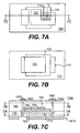
FIGS. 7A-7C illustrate yet another embodiment of an innerlayer
panel 7100, similar to the innerlayer panel 6100 illustrated in FIGS. 6A-6C.
The innerlayer panel 7100 comprises a capacitor 705 and laminate layers
770, 760, and is illustrated in a state after incorporation into a printed
wiring board.
The capacitor 705 comprises a first electrode layer 710, a second
electrode layer 720, and a dielectric 730. A trench 722 electrically isolates
the first electrode layer 710 from the second electrode layer 720.
Referring to FIG. 7A, the first electrode layer 710 comprises a plurality of
elongated electrode portions 715, and a main electrode 717. The first
electrode layer 710 can be selectively trimmed at the elongated electrode
portions 715 in order to control the capacitance provided by the capacitor
705.
Referring to FIGS. 7A and 7C, an electrode portion 715 can be
trimmed without damaging the second electrode layer 720. When one or
more electrode portions 715 are trimmed at the location indicated by the
arrow T, if the trimming laser beam passes thought the dielectric 730 the
laser beam will not damage the second electrode layer 720 because the
second electrode layer 720 does not extend over that part of the dielectric
730. The capacitor innerlayer panel 7100 can be formed in a manner
similar to the capacitor 6100.
FIG. 8A is a top plan view of an electrode arrangement comprising
interdigitated electrodes 810, 812. The electrodes 810, 812 are shown in
isolation in FIG. 8A. A complete innerlayer panel 8100, including a
capacitor 805 comprising the electrodes 810, 812, is illustrated in FIG. 81.
A printed wiring board 8000 having the innerlayer panel 8100 incorporated
therein is illustrated in FIG. 8J. The interdigitated electrode capacitor 805
is trimmable in order to adjust its capacitance.
Referring to FIG. 8A, a first electrode 810 includes a plurality of first
elongated electrode portions 812, connected to a first conductive portion
814. The second electrode 820 includes a plurality of second elongated
electrode portions 822 electrically connected to a second conductive
portion 824. The conductive portions 814, 824 act as terminations for the
electrodes 810, 820, respectively. The first elongated electrode portions
812 are interdigitated with the second elongated electrode portions 822.
The first and second elongated electrode portions 812, 822 are separated
by a space 828 having the shape of a serpentine trench. The electrode
pattern in FIG. 8A may be trimmed for fine capacitance control of the
capacitor 805 (the trimming process is shown in FIG. 8H). The trimming
process and a method of making the capacitor 805 and the innerlayer
panel 8100 are discussed below with reference to FIGS. 8B-8I.
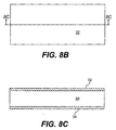
FIG. 8B is a plan view of a first stage of manufacturing the
innerlayer panel 8100. FIG. 8C is a section view in front elevation taken
on line 8C-8C in FIG. 8B. Referring to FIG. 8C, a first foil 32 is provided,
and is laminated to a first side of laminate material 30. The first foil 32
may be of a type generally available in the industry. For example, the foil
32 may be copper, copper-invar-copper, invar, nickel, nickel-coated
copper, or other metals. The foil 32 may correspond to between about 1
oz and 2 oz copper foil. Thick copper foils are preferred because they
form thick electrodes, and provide correspondingly high capacitance
densities. The laminate material 30 may be, for example, FR4 prepreg or
other organic materials. A second foil 34 may also be laminated to a
second side of the laminate material 30.
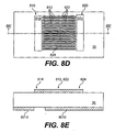
FIG. 8D is a top plan view of a next stage of manufacture. FIG. 8E
is a section view taken on line 8E-8E in FIG. 8D. Referring to FIG. 8D, a
photo-resist is applied to the first foil 32, and the foil 32 is imaged, etched
and stripped. The electrodes 810, 812, including the first and second
elongated electrode portions 812, 814, the serpentine trench 828, and the
conductive portions 814, 824 result from the etching step. The second foil
34 may also be etched to form circuitry 8010. The circuitry 8010 illustrated
in FIG. 8E can act as, for example, a power plane 8010 in the finished
printed wiring board 8000 (illustrated in FIG. 8J).
Referring to FIGS. 8F and 8G, a dielectric layer 38 is applied to the
resulting article. The dielectric layer 38 is applied to fill the serpentine
trench 828 between the elongated electrode portions 812, 822. The
dielectric layer 38 illustrated in FIG. 8F covers the electrode portions 812
and 822. However, a dielectric layer that only fills the trench 828 between
the elongated electrode portions 812, 822, without covering the tops of the
electrode portions, is sufficient. Any additional surface area of the
dielectric layer 38 provides a tolerance for registration issues. The
dielectric layer 38 can be formed from, for example, a polymer thick film
(PTF) paste. The dielectric layer 38 can be applied by, for example,
solution casting or screen printing. The dielectric layer 38 is then cured.
In an interdigitated capacitor design such as is shown in FIGS. 8F
and 8G, the capacitance is proportional to the depth of the electrodes 812,
822, the width of the dielectric-filled trench 828 between the electrodes
812, 822, and the length of the serpentine trench 828. The article shown
FIGS. 8F and 8G has a capacitance that is above a target value. The
capacitance is reduced to the target value by a trimming operation as
described below.
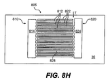
After the dielectric is cured, the dielectric layer 38 and the
elongated electrode portions 812, 822 are selectively trimmed. The
trimming process is illustrated in FIG. 8H. The dielectric layer 38 is not
shown in FIG. 8H to better illustrate the trimming process. The trimming
direction is indicated by the arrow T. A UV-YAG laser is one preferred
laser for trimming. The UV-YAG laser may selectively cut portions of
either or both of the first and second elongated conductive portions 812,
822, thereby reducing the capacitance of the capacitor 805. High
tolerance values can be achieved by the use of relatively short elongated
conductive portions 812, 822.
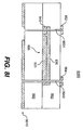
Referring to FIG. 81, a dielectric 830 is illustrated as resulting from
the dielectric layer 38 after the trimming operation. Laminations, etching
and via formation processes, for example, may be used to form circuitry
8010, 862, 864, laminates 850, 860 and circuit conductors 8001, 8002.
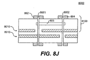
FIG. 8J is a schematic section view of the printed wiring board
8000. The printed wiring board 8000 may be formed by laminating one or
more innerlayer panels together, including the innerlayer panel 8100. The
lamination can be performed in, for example, one or more conventional
lamination pressings. In FIG. 8J, the circuit conductors 8001, 8002
correspond to the through-hole vias illustrated in FIG. 8I. The through- hole
vias 8001, 8002 are preferably drilled and plated after all laminate
layers have been pressed together. The circuitry 8010 may serve as a
power plane. A ground plane 8012 may also be included in the printed
wiring board 8000.
According to the above embodiments, high tolerances may be
achieved by selective trimming of the various electrode arrangements.
In the above embodiments, the thickness of the electrode layers
and the dielectric layers may vary. In general, the thickness of the layers
may fall in the range of about 10-50 microns.
In the above embodiments, other types of circuit conductors may be
used in place of or in addition to through-hole vias. For example,
conductive connections to peripheral edges of electrode layers may be
used in place of through-hole vias.
In the lamination processes described above, laminations can be
performed, for example, using FR4 prepreg in standard printing wiring
board processes. Type 106 epoxy prepreg may also be used. Suitable
lamination conditions are, for example, 185°C at 208 psig for 1 hour in a
vacuum chamber evacuated to about 28 inches of mercury. A silicone
rubber press pad and a smooth PTFE-filled glass release sheet may be in
contact with foils to prevent epoxy from gluing lamination plates together.
The dielectric prepreg and laminate materials can be any type of dielectric
material such as, for example, standard epoxy, high Tg epoxy, polyimide,
polytetrafluoroethylene, cyanate ester resins, filled resin systems, BT
epoxy, and other organic resins and laminates that provide insulation
between circuit layers.
A single capacitor is formed in the innerlayer panels described
above. However, the printed wiring board embodiments can include a
large number of individual capacitors of differing type and arranged in
various ways in the printed wiring boards.
The printed wiring board embodiments discussed above may
include additional innerlayer panels, laminate layers, and other layers.
Additional interconnect circuitry, other passive components, or active
components, may also be included in the printed wiring boards.
The printed wiring board embodiments discussed above may be
formed by fired-on-foil processes or by using polymeric materials. In
polymeric embodiments, Curing can be done at, for example, about
150°C.
Suitable materials for the paste used to form polymeric conductive
layers include, for example, polymer thick-film copper pastes, silver
polymer thick-film pastes, which may include copper or silver powders
dispersed into an organic vehicle. The organic vehicle can be an epoxy
solution or other solutions based on other resins. A commercially
available polymer conductive layer is CB200 available from E. I. du Pont
de Nemours and Company.
Suitable materials for the paste used to form polymer dielectric
layers include polymer thick-film dielectric pastes. Polymer thick-film
dielectric pastes are generally high dielectric constant materials, such as,
for example, barium titanate powder, dispersed into an organic vehicle
such as an epoxy resin. A commercially available high dielectric constant
polymeric dielectric layer is 7153 thick-film dielectric available from
E. I. Du Pont de Nemours and Company. Curing of the conductive and
dielectric layers can be performed at, for example, about 150°C.
The conductive layers discussed in this specification may also be
formed by, for example, electrodeposition processes or evaporation
processes. Electrodeposition processes or evaporation processes can be
used to form, for example, metallic conductive layers. The dielectric layers
may alternatively be formed by, for example, thin film sputtering or
anodizing.
One suitable thick-film dielectric material for use in fired-on-foil
embodiments has the following composition:
| Barium titanate powder | 64.18 % |
| Zirconium oxide powder | 3.78 % |
| Glass A | 11.63 % |
| Ethyl cellulose | 0.86 % |
| TEXANOL | 18.21 % |
| Barium nitrate powder | 0.84 % |
| Phosphate wetting agent | 0.5 %. |
| Glass A: |
| Germanium oxide | 21.5 % |
| Lead tetraoxide | 78.5 %. |
A suitable Glass A composition corresponded to Pb5Ge3O11, which
precipitates out during the firing, and has a dielectric constant of
approximately 70-150. A resulting dielectric after firing has a dielectric
constant of approximately 1000.
A suitable thick-film copper electrode ink for use in fired-on-foil
embodiments has the following composition:
| Copper powder | 55.1 % |
| Glass A | 1.6 % |
| Cuprous oxide powder | 5.6 % |
| Ethyl cellulose T-200 | 1.7 % |
| TEXANOL | 36.0 %. |
Thin film ceramic capacitors can be formed via a number of
processes that yield thin ceramic layers of less than, for example, 1
micron. Examples of such materials include barium titanate or alumina,
which can be deposited by sol-gel techniques or sputtering, for example.
In the fired-on-foil embodiments discussed in this specification, the
term "paste" may correspond to a conventional term used in the electronic
materials industry, and generally refers to a thick-film composition.
Typically, the metal component of the underprint paste is matched to the
metal in the metal foil. For example, if a copper foil were used, then a
copper paste could be used as the underprint. Examples of other
applications would be pairing silver and nickel foils with a similar metal
underprint paste. Thick-film pastes may be used to form both the
underprint and the passive components.
Generally, thick-film pastes comprise finely divided particles of
ceramic, glass, metal or other solids dispersed in polymers dissolved in a
mixture of plasticizer, dispersing agent and organic solvent. Preferred
capacitor pastes for use on copper foil have an organic vehicle with good
burnout in a nitrogen atmosphere. Such vehicles generally contain very
small amounts of resin, such as high molecular weight ethyl cellulose,
where only small amounts are necessary to generate a viscosity suitable
for screen-printing. Additionally, an oxidizing component such as barium
nitrate powder, blended into the dielectric powder mixture, helps the
organic component burn out in the nitrogen atmosphere. Solids are mixed
with an essentially inert liquid medium (the "vehicle"), then dispersed on a
three-roll mill to form a paste-like composition suitable for screen-printing.
Any essentially inert liquid may be used as the vehicle. For example,
various organic liquids, with or without thickening and/or stabilizing agents
and/or other common additives, may be used as the vehicle.
High K thick-film dielectric pastes generally contain at least one
high K functional phase powder and at least one glass powder dispersed
in a vehicle system composed of at least one resin and a solvent. The
vehicle system is designed to be screen-printed to provide a dense and
spatially well-defined film. The high K functional phase powders can
comprise perovskite-type ferroelectric compositions with the general
formula ABO3. Examples of such compositions include BaTiO3; SrTiO3;
PbTiO3; CaTiO3; PbZrO3; BaZrO3 and SrZrO3. Other compositions are
also possible by substitution of alternative elements into the A and/or B
position, such as Pb(Mg1/3 Nb2/3)O3 and Pb(Zn1/3 Nb2/3)O3. TiO2 and
SrBi2Ta2O9 are other possible high K materials.
Doped and mixed metal versions of the above compositions are
also suitable. Doping and mixing is done primarily to achieve the
necessary end-use property specifications such as, for example, the
necessary temperature coefficient of capacitance (TCC) in order for the
material to meet industry definitions, such as "X7R" or "Z5U" standards.
The glasses in the pastes can be, for example, Ca-Al borosilicates,
Pb-Ba borosilicates, Mg-Al silicates, rare earth borates, and other similar
glass compositions. High K glass-ceramic powders, such as lead
germanate ( Pb5Ge3O11) compositions, are preferred.
Pastes used to form conductive layers may be based on metallic
powders of either copper, nickel, silver, silver-containing precious metal
compositions, or mixtures of these compounds. Copper powder
compositions are preferred.
The embodiments described in this specification have many
applications. For example, one or more of the capacitor embodiments can
be used within organic printed circuit boards, IC packages, applications of
said structures in decoupling applications, and devices such as IC
modules and devices or handheld device motherboards.
The foregoing description illustrates and describes the preferred
embodiments of the present invention. It is to be understood that the
invention is capable of use in various other combinations, modifications,
and environments and is capable of changes or modifications within the
scope of the inventive concept as expressed herein, commensurate with
the above teachings, and/or the skill or knowledge of the relevant art.
The embodiments described hereinabove are further intended to
explain best modes known of practicing the invention and to enable others
skilled in the art to utilize the invention in such, or other, embodiments and
with the various modifications required by the particular applications or
uses of the invention. Accordingly, the detailed description is not intended
to limit the invention to the form disclosed herein. Also, it is intended that
the appended claims be construed to include alternative embodiments.