EP1517333B1 - Drapeau pour mémoire asymétrique avec drapeau indicant l'état concernant la proframmarion et l'éffacement - Google Patents
Drapeau pour mémoire asymétrique avec drapeau indicant l'état concernant la proframmarion et l'éffacement Download PDFInfo
- Publication number
- EP1517333B1 EP1517333B1 EP04018551A EP04018551A EP1517333B1 EP 1517333 B1 EP1517333 B1 EP 1517333B1 EP 04018551 A EP04018551 A EP 04018551A EP 04018551 A EP04018551 A EP 04018551A EP 1517333 B1 EP1517333 B1 EP 1517333B1
- Authority
- EP
- European Patent Office
- Prior art keywords
- state
- memory
- identifier
- flag
- value
- Prior art date
- Legal status (The legal status is an assumption and is not a legal conclusion. Google has not performed a legal analysis and makes no representation as to the accuracy of the status listed.)
- Not-in-force
Links
Images

Classifications
-
- G—PHYSICS
- G11—INFORMATION STORAGE
- G11C—STATIC STORES
- G11C16/00—Erasable programmable read-only memories
- G11C16/02—Erasable programmable read-only memories electrically programmable
- G11C16/06—Auxiliary circuits, e.g. for writing into memory
- G11C16/10—Programming or data input circuits
- G11C16/14—Circuits for erasing electrically, e.g. erase voltage switching circuits
- G11C16/16—Circuits for erasing electrically, e.g. erase voltage switching circuits for erasing blocks, e.g. arrays, words, groups
-
- G—PHYSICS
- G11—INFORMATION STORAGE
- G11C—STATIC STORES
- G11C16/00—Erasable programmable read-only memories
- G11C16/02—Erasable programmable read-only memories electrically programmable
- G11C16/06—Auxiliary circuits, e.g. for writing into memory
- G11C16/10—Programming or data input circuits
Definitions
- the invention relates to a memory device having an asymmetrical electronic memory having a plurality of memory cells with at least one state flag implemented in the memory, which optionally has a first (set, valid) state value or a second (unset, invalid) state value, and that is switchable between the first and the second state value.
- An electronic memory is usually divided into a plurality of memory cells.
- the individual memory cells are brought from a first memory state, for example a logical "1", to a second memory state, for example a logical "0", and vice versa, for which erasures and writes are performed.
- Which state of the deleted and the described memory state while a logical "1" and which is a logical "0" is usually arbitrary and is usually already determined by the manufacturer of the memory.
- a plurality of electronic memories are asymmetric in writing and erasing data, for example, by making the time required for erasing the memory (erasing time or erasing time) different from the amount of time required to write to the memory (write time or write duration).
- the power consumption during writing may be different from the power consumption when deleting.
- the programming voltage to be applied for programming is different, depending on whether the memory is written or deleted.
- the programming voltage here is to be understood as meaning the voltage actually applied to the memory cell which may be different from an external voltage generated by a voltage source which is used to generate the programming voltage.
- a state flag or equivalent flag For example, depending on the state value (flag value), writing (or reading) in the memory section may be either prohibited or allowed.
- the subject matter of the invention is a status code or flag in this sense, that is to say a code by which a status is indicated.
- flags are often used in so-called atomic writes, which are characterized by being either only complete or not at all.
- An example of such an atomic write operation is the writing of data into a smart card, for example, to update an erroneous counter or to charge an electronic purse with a payment ( Rankl, Effing, Handbuch der Chip Actually, 4th edition, Carl Hanser Verlag Kunststoff Vienna, 2002, chapter 5.10 "Atomic Processes", pp. 293-295 ). If new data is to be written into a memory section of the chip card, first the original data, which are stored in the memory section before writing, is copied into a non-volatile buffer memory of the chip card (eg into an EEPROM memory of the chip card).
- the state flag or flag has a valid state value in this case.
- the new data for example, new amount of money in the electronic purse that is equal to the originally existing amount of money reduced by the amount to be paid
- the status flag (flag ) be used to restore the memory contents of the memory portion of the smart card when needed. If the state flag of the buffer memory is set, ie "set to valid", the data from the buffer memory, ie the original data, is written back into the memory section, since previously the new data has not yet been completely programmed in. The new data must be re-registered. In the case of an electronic wallet, therefore, the amount of money that was there before the partially failed debit process (reduction of the amount of money) there was restored in the electronic purse. The load must be repeated.
- State flags are also used in a variety of other different operations except for atomic writes and reads.
- a conventional state flag consists of a single memory cell, e.g. a single bit set to zero "0" or one "1" depending on whether the state flag state flag is valid (flag set) or invalid (flag not set).
- the memory cells contain a material that can assume an amorphous and a crystalline state, one of which corresponds to the described and the other to the erased state. Because switching the material from the amorphous to the crystalline state takes different amounts of time than vice versa, the memory is asymmetrical with respect to writes and erasures.
- a memory device according to the preamble of claims 1 and 16 is known from US 5996041 known.
- the object of the invention is to provide a memory device of the type mentioned, which allows a more efficient switching of the state flag, and to provide a corresponding identification method using a state flag.
- the memory device according to the invention according to the independent claim 1, or the inventive method according to independent claim 16, has, or refers to an electronic memory having a plurality of binary memory cells.
- Each memory cell is switchable by a programming operation between an erased and a written state, wherein by an erase operation, the erased state can be produced and by a write operation of the described state can be produced.
- the memory is asymmetric with respect to writes and erasures, which means in more detail that one or more program parameters have a different (different) value in a write operation than in an erase operation.
- the programming parameters may include: the programming duration, ie the time required to perform a complete programming operation, in particular writing or erasing; the programming voltage, ie the voltage that has to be applied to the memory, in particular to each individual memory cell, in order to carry out a programming operation.
- the memory is further implemented with at least one state flag which may optionally have a first (set, valid) state value or a second (deleted, invalid, not set) state value.
- the memory device has a switching device with which the value of the state identifier can be switched between the first and the second state value, at least one programming process being performed on at least one memory cell for switching the state value.
- the switching means with which the value of the state flag can be switched ie selectively set and cleared, is implemented such that the same type of programming operation for switching from the first to the second state value and to the switching from the second to the first state value Write or delete operation is performed.
- a write operation is performed on a memory cell.
- an erase operation is performed on a memory cell.
- the memory device has the advantage that the state flag (flag) is symmetrical with respect to its setting and erasing. That In particular, the one or more programming parameters such as program duration and / or program voltage have the same value when cleared and set. As a result, no case discrimination needs to be made on whether the flag is set or cleared, so that a switch can be used with a simple structure. The switching of the state flag is thereby more efficient than in known memory devices.
- a memory device which enables a more efficient switching of the state flag.
- precisely one programming operation is carried out on exactly one memory cell for setting and for deleting the status code (flag).
- the memory may be, for example, an EEPROM or a Flash EEPROM (Flash ROM), which is asymmetric in the above sense.
- the components of the memory device according to the invention can be implemented in software form, in hardware form or partly in software form, partly in hardware form.
- the state identifier and the switching device and possibly other components are implemented in software form.
- the asymmetry with respect to write operations and deletions comprises, according to an embodiment of the invention, a write operation of a has a shorter programming time (shorter) than a deletion or vice versa.
- the switching means for switching between the first and second state values of the flag (Flag) uses the programming operation of the writing operation and the erasing operation having a shorter programming period.
- This preferred embodiment has the further advantage that the state flag only uses "fast" programming operations to switch its state value. As a result, the state indicator is particularly time-saving and therefore efficient.
- the asymmetry of writes and erasures involves a write requiring a different (higher or lower) program voltage than an erase.
- a different program voltage Preferably, when switching the state flag that programming operation is used which requires the lower programming voltage.
- This preferred embodiment has the further advantage that the state flag is particularly energy-saving when switching its state value.
- the memory device further has a reset device, with which an output state of the state flag is adjustable.
- a reset device Starting from the initial state, at least one switching operation for switching, in particular setting or clearing, of the state flag (flag) is possible.
- a plurality of successive switching operations is possible starting from the initial state in which the state value of the state flag alternately between valid and invalid, ie alternately always from invalid to valid and once from valid to invalid is switched. In doing so, According to the invention, the same type of programming operation is used for switching, regardless of whether the state flag is switched to valid or to invalid.
- the reset means is also preferably implemented to use the other programming operation of the write and erase operations to set the output state than is used to switch between the first and second state values of the flag.
- a write operation to a memory cell is used to switch the state flag (Flag) and an erase operation is used to set the output state by means of the reset device or vice versa.
- the faster programming operation is used, in which the programming time is lower, whereas for setting the initial state by means of the reset means the slower programming operation is used, in which the programming time is higher.
- the slow programming operation is applied exclusively to the reset, which is usually performed less frequently than the switching of the state flag. In the usually more frequent switching of the state flag, i. when setting and deleting, the fast programming process is used.
- the state flag (Flag) of the power-saving programming process is used, in which a lower programming voltage must be applied to the memory cell (s), whereas to set the output state by means of the reset means the more current-intensive programming operation is used, in which a higher programming voltage must be applied to the memory cell (s).
- the power-intensive programming operation is only in the rare reset the state flag (flag) in use, when switching (set, clear) of the state flag (Flag), however, the power-saving programming process is used.
- a preferred use of the memory device according to the invention is in a data carrier such as a chip card or a token, with an electronic circuit in which the memory device is implemented.
- the chip card can be a contactless or contact-type or both contactless and contact-operated chip card of any format, e.g. according to ISO 7810, e.g. ID-1 (credit card size) or ID-000 (SIM card or mini-card format) or ID-00 or GSM 11.1 or TS 102.221 or other standard, or no standard.
- the token can have any housing and any interface (contactless, contact-type, serial, USB, etc.).
- the state tag has at least one pair of two sub-tags, each sub-tag of the pair having at least one memory cell.
- the state indicator off Fig. 1 which will be described in more detail below, forms a special form of such state flag, in which in particular each sub-tag of the pair has the same number of memory cells, in particular eight.
- the part indicators Fig. 1 are formed of individual memory cells, each memory cell being one bit in size, so that each sub-tag is formed as bit field B1 or B2.
- the individual memory cells may have a size other than bits, for example, each memory cell may be two bits or one byte in size.
- the number of memory cells per subfield may also be higher or lower than eight.
- the number of memory cells per sub tag / bit field unlike in Fig. 1 shown to be different.
- the number of memory cells in both sub-flags is the same, since in this case alternating switching of the state flag in the two sub-flags / bit fields to the last memory cell is possible.
- a flash memory according to the invention with the status code with the two partial identifiers is preferably divided into pages, with one page being deleted at a time when the memory is deleted.
- Each of the two sub-flags preferably has a number of memory cells equal to an integer divisor of the page size (number of memory cells per page) in the flash memory, so that a single page can be completely filled by an integer number of sub-flags.
- the size of the partial identifier (number of memory cells in the partial identifier) is equal to an integer divisor of half the page size, so that a single page can be completely filled by an integer number of state identifiers with two partial identifiers.
- the first state value is characterized in that in each sub-flag of the pair, the same number of memory cells have the erased and / or described states, the second state value in this embodiment it is excellent that in each sub-tag of the pair, a different number of memory cells have the erased and / or described state.
- the individual memory cells of the first partial identifier form with the individual memory cells of the second partial identifier pairs of corresponding memory cells, ie the first (second, third, fourth,...) Memory cell of the first partial identifier corresponds to the first (second, third, fourth, ...) memory cell of the second part identifier.
- the first state value is distinguished in that corresponding memory cells have the same state in the two partial identifiers
- the second state value is distinguished by the fact that in the two partial identifiers in a pair of corresponding memory cells, the two corresponding memory cells have a different state.
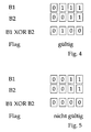
- Fig. 1 shows a state flag according to a preferred embodiment of the invention.
- the state flag (Flag) consists of two bit fields B1, B2 each with eight bits.
- the first line a) of Fig. 1 shows the state flag (Flag) in its initial state, in which it is after a reset by means of the reset means, without having been switched again after resetting. All bits have the logic value "1", so that both bit fields B1, B2 have the same number of eight “ones" and zero "zeroes".
- each pair of corresponding bits (memory cells) of the two bit fields B1, B2 has the same state, ie the first bit (from left) of the first bit field B1 has the same state as the first bit (from left) of the second bit field B2, the second bit (from left) of the first bit field B1 has the same state as the second bit (from the left) of the second bit field B2, the third bit (from the left) of the first bit field B1 has the same state as the third bit (from the left) of the second bit field B2 etc.
- the state value of the state flag (flag) is not valid, ie the flag is cleared, ie not set.
- the second line b) of Fig. 1 shows the state flag after it has been set, ie after its state value has been set to "set".
- the first bit of the first bit field B1 (framed) has been switched from “1" to "0".
- the bit field B1 now has seven ones and one zero.
- the state value of the state flag is consequently valid or set.
- the first bit of the first bit field B1 (state value "0") has a different state than the first bit of the second bit field B2 (state value "1").
- the state flag (Flag) also set according to this criterion (valid).
- the third line c) of Fig. 1 shows the state flag after it has been cleared again after being set from line b), ie, after its state value has been set to not set (cleared).
- the first bit of the second bit field B2 (framed) has been switched from “1" to "0".
- the first bit field B1 still has seven ones and one zero.
- the second bit field B2 now also has seven ones and a zero. Therefore, the two bit fields B1, B2 have the same number of ones and zeros, respectively.
- the state value of the state flag is thus invalid or not set.
- line c) of Fig. 1 the first bit of the first bit field B1 and the first bit of the second bit field B2 (again) the same state.
- the first pair of corresponding bits (memory cells) thus has (again) the same state, so that all corresponding bits (memory cells) have the same state.
- the fourth line d) of Fig. 1 shows the state flag after it has been reset, following deletion from line c).
- the second bit of the first bit field B1 (framed) has been switched from "1" to "0". Therefore, the two bit fields B1, B2 have a different number of ones. The state value of the state flag is thus invalid or not set.
- the second bit of the first bit field B1 (framed, state value "0") and the second bit of the second bit field B2 (state value "1") have a different one Status.
- the corresponding second bits of the two bit fields B1, B2 thus have a different state. All other corresponding pairs (first, third, fourth, ... eighth corresponding pair) of bits each have the same state, namely to the left of the current (here second) bit with state value "1", to the right of state value "0".
- the state flag can be set six more times and deleted seven times, ie a total of eight times, ie as many as each bit field has bits, set and deleted.
- one bit in the first bit field B1 and one bit in the second bit field B2 are alternately switched.
- the adjacent bits are switched in sequence, ie first the first bit, then the second bit, then the third bit, then the fourth bit etc.
- the last bit as in the last line o ) from Fig. 1 is shown, the last bit (framed) of the second bit field B2 switched. Only then are all bits set to "zero", and the state flag must be reset (reset) to that in line a) of Fig. 1 restore restored state.
- the memory device has a logic unit, in particular an XOR logic unit, from the configuration of the partial identifiers (bit fields).
- the logic unit is set up to link corresponding memory cells of the first and the second component identifier and to output the result of the combination as the status value of the status identifier.
- FIG. 4 and FIG. 5 illustrate the operation of a logic unit according to the invention in the form of an XOR logic unit.
- Fig. 4 shows the operation of an XOR logic unit using the example of a valid (set) flag.
- Fig. 5 shows how the XOR logic unit works using the example of an invalid (not set, deleted) flag.
- the first two lines of the FIGS. 4 and 5 each show a state flag with two bit fields B1 and B2 according to a similar embodiment of the state flag as in FIG Fig. 1 shown, but with only four bits per bit field B1, B2.
- the flag off Fig. 4 is set (valid) since the second bit of the first memory field B1 has the state value "1" and the second bit of the second memory field B2 has the state value "0", so that the two corresponding second bits have different state values.
- the bitwise XOR combination of the two bit fields results in the bit sequence shown in the third line. Since one of the four bits, here the second bit, is different from zero, the flag is considered set (valid), as shown in the fourth line. The flag would be considered set even if, in the third row, another one of the four bits, that is, the first, third or fourth bit, would be different from zero (in Fig. 4 Not shown).
- the flag off Fig. 5 is not set (invalid) since all four pairs of corresponding bits have the same state value, namely "zero" for the two corresponding first bits and the two corresponding second bits, and "one" for the two corresponding third bits and the two corresponding ones fourth bits.
- the bitwise XOR combination of the two bit fields results in the bit sequence shown in the third line. Since all bits are zero, the flag is considered not set (invalid), as shown in the fourth line.
- Fig. 2 shows, according to one embodiment of the invention, the process flow when writing (copying) new data to a file, with prior buffering of the original data that was originally present in the file.
- Fig. 3 schematically shows the temporal and spatial sequence of the copying processes in the process Fig. 2 ,
- a file contains original data. Now, new data will be copied to the file and saved there, overwriting the original data.
- a buffer is available that has a flag that allows the data in the buffer to be marked as valid or invalid.
- the original data of the file is copied into the buffer memory ( Fig. 2, Fig. 3 ).
- the flag of the buffer memory is set to valid ( Fig. 2 ). This can be done, for example, by a switching operation (2) like that in line b) of Fig. 1 are shown, in which the first bit of the first bit field B1 is switched.
- a third step (3) the new data is copied to the file and stored there ( Fig. 2, Fig. 3 ).
- a fourth step (4) the buffer memory flag is set to invalid ( Fig. 2 ). This can, for example, by a switching operation (4) as in line c) of Fig. 1 are shown, in which the first bit of the second bit field B2 is switched. If a process aborts while the flag is set, resuming the process writes the data from the buffer to the file. If, on the other hand, the flag is cleared when the process aborts, the data contained in the file will be retained when the process is resumed.
- a first step (5) the original data of the file is copied to the buffer ( Fig. 2, Fig. 3 ).
- step (6) the flag of the buffer memory is set to valid ( Fig. 2 ). This can be done, for example, by a switching process (6) like that in line d) of Fig. 1 are shown, in which the second bit of the first bit field B1 is switched.
- the memory device further additionally has a reset safety unit, which is set up to check the state flag for consistency in accordance with a predetermined structure having the state flag.
- the reset protection unit can prevent the flag from reaching an indeterminate state if, during operation, e.g. during the set or reset, an interruption occurs, in particular an interruption of the supply voltage. Which state of the state flag is consistent and which is not is predetermined by the structure of the state flag.
- the consistency preferably comprises, within each sub-tag, at most a single pair of adjacent memory cells having different state values. In this way, it is ensured that the memory cells have values as generated by a proper bitwise, sequential write in which adjacent memory cells within a sub-tag are sequentially (ie, in an order first, second, third, etc. memory cell ).
- the reset security unit is preferably further configured to cause or effect a reset of the state flag to the initial value if the check results in a lack of consistency. If the reset is effected, preferably all facilities required for this purpose are present at the memory device, and further preferably integrated in a data carrier such as a chip card or a token. If the reset is merely initiated, optionally at least a portion of the devices required to effect the reset are provided separately from the memory device and, if the memory device is integrated with a data carrier such as a smart card or a token, external to the data carrier.
- the status flag is recognized as inconsistent.
- the status code is reset to the initial value (eg "11111111").
- a logically linear arrangement of the memory cells is understood to mean that the memory cells are logically juxtaposed so that they form a linear sequence of memory cells, for example a memory word or a plurality of memory words or the like, wherein the memory cells do not necessarily have to be physically adjacent to one another.
- a write operation preferably has a write duration in the range of about 1 to about 20 ⁇ s, more preferably about typically 7 ⁇ s and a maximum of 10 ⁇ s
- an erase operation has an erase duration in the range of about 1 ms to about 50 ms, more preferably typically about 18 ms and a maximum of 25 ms, or vice versa.
- the programming voltage is preferably for writing in the voltage range of 1V to 4V, preferably at about 3.0V to 3.6V and for erasing in the voltage range of 5V to 16V, preferably at about 10V, or vice versa.
- the programming voltage is preferably equal to the voltage applied to the single memory cell voltage, which may be different from the externally applied voltage, wherein the voltage applied to the memory cell is preferably generated in a conventional manner from the externally applied voltage.
- the externally applied voltage is, for example, the output voltage of a voltage source.
- the mentioned parameter values are example values. Depending on the memory used, the parameter values may also be in other ranges.
Claims (19)
- Dispositif de mémoire avec- une mémoire électronique comportant une pluralité de cellules de mémoire binaires, chaque cellule de mémoire étant, par un processus de programmation, commutable entre un état dans lequel les données sont effacées et un état dans lequel les données figurent, l'état dans lequel les données sont effacées pouvant être produit par un processus d'effacement et l'état dans lequel les données figurent pouvant être produit par un processus d'écriture, la mémoire étant asymétrique quant aux processus d'effacement et aux processus d'écriture, cela signifiant plus précisément qu'un ou plusieurs paramètres de programmation ont une autre valeur lors d'un processus d'écriture que lors d'un processus d'effacement,
le dispositif de mémoire étant en outre équipé de- au moins un indicateur d'état (Flag B1, B2) implémenté dans la mémoire, qui peut avoir au choix une première valeur d'état positionnée ou une deuxième valeur d'état non positionnée, l'indicateur d'état (B1, B2) comprenant au moins deux indicateurs partiels, et- un dispositif de commutation, avec laquelle la valeur de l'indicateur d'état (B1, B2) est commutable entre la première et la deuxième valeur d'état, au moins un processus de programmation étant effectué à au moins une cellule de mémoire pour commuter la valeur d'état,caractérisé en ce que le dispositif de commutation est implémenté de telle sorte que, pour commuter l'indicateur d'état (B1, B2) de la première à la deuxième valeur d'état et pour commuter de la deuxième à la première valeur d'état, le même mode de processus de programmation, soit processus d'écriture, soit processus d'effacement, est effectué dans les deux cas. - Dispositif de mémoire selon la revendication 1, l'asymétrie relative aux processus d'écriture et processus d'effacement incluant qu'un processus d'écriture a une durée de programmation plus courte qu'un processus d'effacement ou inversement.
- Dispositif de mémoire selon la revendication 1 ou 2, le processus de programmation du processus d'écriture et du processus d'effacement utilisé par le dispositif de mémoire pour commuter entre la première et la deuxième valeur d'état de l'indicateur d'état (Flag B1, B2) étant celui qui a une durée de programmation plus courte.
- Dispositif de mémoire selon une des revendications de 1 à 3, l'asymétrie relative aux processus d'écriture et processus d'effacement incluant qu'un processus d'écriture a besoin d'une autre tension, notamment d'une tension plus élevée ou plus basse, qu'un processus d'effacement, notamment pour le processus de programmation à la cellule de mémoire.
- Dispositif de mémoire selon une des revendications de 1 à 4, l'indicateur d'état (B1, B2) ayant au moins une paire de deux indicateurs partiels (B1, B2), chaque indicateur partiel de la paire comportant au moins une cellule de mémoire.
- Dispositif de mémoire selon la revendication 5, chaque indicateur partiel (B1, B2) de la paire ayant le même nombre de cellules de mémoire.
- Dispositif de mémoire selon la revendication 5 ou 6, la première valeur d'état de l'indicateur d'état (Flag B1, B2) se distinguant par le fait que, dans chaque indicateur partiel de la paire d'indicateurs partiels (B1, B2), le même nombre de cellules de mémoire a l'état dans lequel les données sont effacées et / ou l'état dans lequel les données figurent, et la deuxième valeur d'état de l'indicateur d'état (Flag B1, B2) se distinguant par le fait que, dans chaque indicateur partiel de la paire d'indicateurs partiels (B1, B2), un nombre différent de cellules de mémoire a l'état dans lequel les données sont effacées et / ou l'état dans lequel les données figurent.
- Dispositif de mémoire selon une des revendications de 5 à 7, la première valeur d'état de l'indicateur d'état (Flag B1, B2) se distinguant par le fait que, dans les deux indicateurs partiels de la paire d'indicateurs partiels (B1, B2), des cellules de mémoire correspondantes ont le même état, et la deuxième valeur d'état de l'indicateur d'état (Flag B1, B2) se distinguant par le fait que, pour une paire de cellules de mémoire correspondantes dans les deux indicateurs partiels (B1, B2), les deux cellules de mémoire correspondantes ont des états différents l'un de l'autre.
- Dispositif de mémoire selon une des revendications de 5 à 8, qui comporte un boîtier logique notamment implémenté sous forme de logiciel et / ou sous forme de matériel, notamment un boîtier logique XOR, qui est équipé pour chaîner des cellules de mémoire correspondantes du premier et du deuxième indicateur partiel (B1, B2) et délivrer le résultat du chaînage en tant que valeur d'état de l'indicateur d'état (B1, B2) ou mettre à disposition le résultat du chaînage pour la poursuite du calcul de la valeur d'état.
- Dispositif de mémoire selon une des revendications de 1 à 9, qui comporte en outre un dispositif de réinitialisation, avec lequel un état initial de l'indicateur d'état (B1, B2) est réglable.
- Dispositif de mémoire selon la revendication 10, le dispositif de réinitialisation étant implémenté de telle façon que, pour régler l'état initial, il utilise l'autre processus de programmation du processus d'écriture et du processus d'effacement, et non celui qui est utilisé pour commuter entre la première et la deuxième valeur d'état de l'indicateur d'état (Flag B1, B2).
- Dispositif de mémoire selon la revendication 10 ou 11, qui comporte en outre une unité de protection de réinitialisation équipée pour vérifier l'indicateur d'état (B1, B2) quant à sa consistance en fonction d'une structure prédéterminée qu'a l'indicateur d'état.
- Dispositif de mémoire selon la revendication 12, l'unité de protection de réinitialisation étant équipée pour entraîner ou pour occasionner une remise de l'indicateur d'état (B1, B2) à la valeur initiale quand la vérification décèle une consistance manquante.
- Dispositif de mémoire selon la revendication 12 ou 13, la consistance comprenant, dans le cas d'un indicateur d'état (B1, B2) comportant deux indicateurs partiels (B1, B2) avec chacun plusieurs cellules de mémoire disposées de manière linéaire logique, qu'au maximum une seule paire de cellules de mémoire voisines ayant des valeurs d'état différentes existe à l'intérieur de chaque indicateur partiel.
- Support de données, notamment carte à puce ou jeton, comportant un circuit électronique avec un dispositif de mémoire y étant implémenté selon une des revendications de 1 à 14.
- Procédé d'indication de l'état d'une portion de mémoire contenant notamment un fichier ou un champ de données ou un contenu de mémoire similaire, au moyen d'un indicateur d'état, dans lequel- un dispositif de mémoire avec un indicateur d'état (B1, B2) y étant implémenté est mis à la disposition de la portion de mémoire, et+ au moyen d'une mémoire électronique comportant une pluralité de cellules de mémoire binaires, chaque cellule de mémoire étant, par un processus de programmation, commutable entre un état dans lequel les données sont effacées et un état dans lequel les données figurent, l'état dans lequel les données sont effacées pouvant être produit par un processus d'effacement et l'état dans lequel les données figurent pouvant être produit par un processus d'écriture, la mémoire étant asymétrique quant aux processus d'effacement et aux processus d'écriture, cela signifiant plus précisément qu'un ou plusieurs paramètres de programmation ont une autre valeur lors d'un processus d'écriture que lors d'un processus d'effacement,+ au moyen d'au moins l'indicateur d'état (Flag B1, B2) implémenté dans la mémoire, qui peut avoir au choix une première valeur d'état positionnée ou une deuxième valeur d'état non positionnée, l'indicateur d'état (B1, B2) comprenant au moins deux indicateurs partiels, et+ au moyen d'un dispositif de commutation, avec lequelle la valeur de l'indicateur d'état (B1, B2) est commutable entre la première et la deuxième valeur d'état, au moins un processus de programmation étant effectué à au moins une cellule de mémoire pour commuter la valeur d'état,- dans lequel, en fonction de l'état de la portion de mémoire, l'indicateur d'état (B1, B2) est commuté sur une première valeur d'état ou sur une deuxième valeur d'état,caractérisé en ce que, pour commuter l'indicateur d'état (B1, B2) de la première à la deuxième valeur d'état et pour commuter de la deuxième à la première valeur d'état, le même mode de processus de programmation, notamment soit le processus d'écriture, soit le processus d'effacement, est effectué dans les deux cas.
- Procédé selon la revendication 16, l'indicateur d'état (B1, B2) étant remis à une valeur initiale après commutation unique ou réitérée, la remise étant effectuée de préférence au moyen de l'autre mode de processus de programmation du processus d'écriture et du processus d'effacement, et non au moyen de celui qui est utilisé pour commuter.
- Procédé selon la revendication 17, une vérification de consistance étant en outre effectuée, lors de laquelle l'indicateur d'état (B1, B2) est vérifié quant à sa consistance en fonction d'une structure prédéterminée qu'a l'indicateur d'état (B1, B2).
- Procédé selon la revendication 18, une remise de l'indicateur d'état (B1, B2) à la valeur initiale étant entraînée ou occasionnée quand la vérification de consistance décèle une consistance manquante.
Applications Claiming Priority (2)
| Application Number | Priority Date | Filing Date | Title |
|---|---|---|---|
| DE10336225A DE10336225B3 (de) | 2003-08-07 | 2003-08-07 | Zustandskennzeichen (Flag) für einen bezüglich Löschen und Schreiben asymmetrischen Speicher |
| DE10336225 | 2003-08-07 |
Publications (2)
| Publication Number | Publication Date |
|---|---|
| EP1517333A1 EP1517333A1 (fr) | 2005-03-23 |
| EP1517333B1 true EP1517333B1 (fr) | 2009-12-30 |
Family
ID=33521553
Family Applications (1)
| Application Number | Title | Priority Date | Filing Date |
|---|---|---|---|
| EP04018551A Not-in-force EP1517333B1 (fr) | 2003-08-07 | 2004-08-05 | Drapeau pour mémoire asymétrique avec drapeau indicant l'état concernant la proframmarion et l'éffacement |
Country Status (3)
| Country | Link |
|---|---|
| EP (1) | EP1517333B1 (fr) |
| AT (1) | ATE453913T1 (fr) |
| DE (2) | DE10336225B3 (fr) |
Families Citing this family (1)
| Publication number | Priority date | Publication date | Assignee | Title |
|---|---|---|---|---|
| DE102007059142B3 (de) * | 2007-12-07 | 2008-10-30 | Giesecke & Devrient Gmbh | Verfahren zum Speichern eines Datums in einer Speichereinrichtung und Speichereinrichtung |
Family Cites Families (4)
| Publication number | Priority date | Publication date | Assignee | Title |
|---|---|---|---|---|
| SE320230B (fr) * | 1968-03-11 | 1970-02-02 | Saab Scania Ab | |
| FR2725055A1 (fr) * | 1994-09-28 | 1996-03-29 | Trt Telecom Radio Electr | Dispositif de calculs d'operations modulaires et carte a puce comportant un tel dispositif |
| KR0172366B1 (ko) * | 1995-11-10 | 1999-03-30 | 김광호 | 불휘발성 반도체 메모리 장치의 독출 및 프로그램 방법과 그 회로 |
| US20030128646A1 (en) * | 2002-01-09 | 2003-07-10 | Peter Nangle | Asymmetrical programming mechanism for non-volatile memory |
-
2003
- 2003-08-07 DE DE10336225A patent/DE10336225B3/de not_active Expired - Fee Related
-
2004
- 2004-08-05 EP EP04018551A patent/EP1517333B1/fr not_active Not-in-force
- 2004-08-05 AT AT04018551T patent/ATE453913T1/de not_active IP Right Cessation
- 2004-08-05 DE DE502004010577T patent/DE502004010577D1/de active Active
Also Published As
| Publication number | Publication date |
|---|---|
| EP1517333A1 (fr) | 2005-03-23 |
| DE10336225B3 (de) | 2005-01-13 |
| ATE453913T1 (de) | 2010-01-15 |
| DE502004010577D1 (de) | 2010-02-11 |
Similar Documents
| Publication | Publication Date | Title |
|---|---|---|
| DE4309814C2 (de) | Nichtflüchtige Halbleiterspeichervorrichtung | |
| DE69719968T2 (de) | Stabilisierkreise für mehrere digitale bits | |
| DE19983565B4 (de) | Interner Auffrisch-Modus für eine Flash-Speicherzellenmatrix | |
| EP1089219B1 (fr) | Méthode de proteger une mémoire de donnée | |
| DE10159901B4 (de) | Mikrocomputer mit eingebautem programmierbarem, nichtflüchtigem Speicher | |
| DE102005020797A1 (de) | Nichtflüchtiges Speicherbauelement und Programmierverfahren | |
| EP0195885B1 (fr) | Procédé et dispositif pour l'emmagasinage non volatil de l'état du compte d'un circuit de comptage électronique | |
| DE3318123A1 (de) | Schaltungsanordnung mit einem datenspeicher und einer ansteuereinheit zum auslesen, schreiben und loeschen des speichers | |
| DE102009033961A1 (de) | Emulation eines einmal programmierbaren Speichers | |
| EP0123177B1 (fr) | Méthode et appareil pour commander une mémoire non volatile écriture/lecture d'utilisation | |
| EP1352318B1 (fr) | Circuit integre a microprocesseur pour support de donnees portatif | |
| DE4302553A1 (en) | High security binary counting method for chip card - offsetting final state of binary number w.r.t. sequence such that contents of counter never represents number smaller than previous value | |
| DE4042161C2 (fr) | ||
| EP0070461B1 (fr) | Compteur à mémoire non volatile | |
| EP1517333B1 (fr) | Drapeau pour mémoire asymétrique avec drapeau indicant l'état concernant la proframmarion et l'éffacement | |
| DE60034103T2 (de) | System und Verfahren zur Handhabung einer Unterbrechung der Versorgungsspannung in einem nichtflüchtigen Speicher | |
| DE10321104B4 (de) | Verfahren zur Ablage von veränderlichen Daten | |
| EP1559111B1 (fr) | Procede de fonctionnement d'un ensemble memoire | |
| DE602004008170T2 (de) | Speicherschaltung mit nichtflüchtigem Identifikationsspeicher und zugehöriges Verfahren | |
| DE69820080T2 (de) | Verfahren zum schreiben von binären datenwörtern mittels elektrisch-programmierbarer und löschbarer speicherzellen | |
| EP1564754B1 (fr) | Procédé et dispositif pour gérer des données dans une mémoire non-volatile | |
| EP1308842B1 (fr) | Procédé et dispositif pour la gestion d'une mémoire | |
| DE4220877C2 (de) | Verfahren für nichtflüchtige, lösch- und programmierbare Speichereinrichtungen | |
| EP0214390A1 (fr) | Procédé et dispositif pour libérer une mémoire utilisateur à accès contrôlé | |
| DE19731954C2 (de) | Verfahren zur Erkennung von fehlprogrammierten Speicherzellen eines Speichers |
Legal Events
| Date | Code | Title | Description |
|---|---|---|---|
| PUAI | Public reference made under article 153(3) epc to a published international application that has entered the european phase |
Free format text: ORIGINAL CODE: 0009012 |
|
| AK | Designated contracting states |
Kind code of ref document: A1 Designated state(s): AT BE BG CH CY CZ DE DK EE ES FI FR GB GR HU IE IT LI LU MC NL PL PT RO SE SI SK TR |
|
| AX | Request for extension of the european patent |
Extension state: AL HR LT LV MK |
|
| 17P | Request for examination filed |
Effective date: 20050923 |
|
| AKX | Designation fees paid |
Designated state(s): AT BE BG CH CY CZ DE DK EE ES FI FR GB GR HU IE IT LI LU MC NL PL PT RO SE SI SK TR |
|
| 17Q | First examination report despatched |
Effective date: 20051121 |
|
| GRAP | Despatch of communication of intention to grant a patent |
Free format text: ORIGINAL CODE: EPIDOSNIGR1 |
|
| GRAJ | Information related to disapproval of communication of intention to grant by the applicant or resumption of examination proceedings by the epo deleted |
Free format text: ORIGINAL CODE: EPIDOSDIGR1 |
|
| GRAP | Despatch of communication of intention to grant a patent |
Free format text: ORIGINAL CODE: EPIDOSNIGR1 |
|
| GRAS | Grant fee paid |
Free format text: ORIGINAL CODE: EPIDOSNIGR3 |
|
| GRAA | (expected) grant |
Free format text: ORIGINAL CODE: 0009210 |
|
| AK | Designated contracting states |
Kind code of ref document: B1 Designated state(s): AT BE BG CH CY CZ DE DK EE ES FI FR GB GR HU IE IT LI LU MC NL PL PT RO SE SI SK TR |
|
| REG | Reference to a national code |
Ref country code: GB Ref legal event code: FG4D Free format text: NOT ENGLISH |
|
| REG | Reference to a national code |
Ref country code: CH Ref legal event code: EP |
|
| REG | Reference to a national code |
Ref country code: IE Ref legal event code: FG4D |
|
| REF | Corresponds to: |
Ref document number: 502004010577 Country of ref document: DE Date of ref document: 20100211 Kind code of ref document: P |
|
| PG25 | Lapsed in a contracting state [announced via postgrant information from national office to epo] |
Ref country code: SE Free format text: LAPSE BECAUSE OF FAILURE TO SUBMIT A TRANSLATION OF THE DESCRIPTION OR TO PAY THE FEE WITHIN THE PRESCRIBED TIME-LIMIT Effective date: 20091230 Ref country code: FI Free format text: LAPSE BECAUSE OF FAILURE TO SUBMIT A TRANSLATION OF THE DESCRIPTION OR TO PAY THE FEE WITHIN THE PRESCRIBED TIME-LIMIT Effective date: 20091230 |
|
| REG | Reference to a national code |
Ref country code: NL Ref legal event code: VDEP Effective date: 20091230 |
|
| PG25 | Lapsed in a contracting state [announced via postgrant information from national office to epo] |
Ref country code: PL Free format text: LAPSE BECAUSE OF FAILURE TO SUBMIT A TRANSLATION OF THE DESCRIPTION OR TO PAY THE FEE WITHIN THE PRESCRIBED TIME-LIMIT Effective date: 20091230 Ref country code: SI Free format text: LAPSE BECAUSE OF FAILURE TO SUBMIT A TRANSLATION OF THE DESCRIPTION OR TO PAY THE FEE WITHIN THE PRESCRIBED TIME-LIMIT Effective date: 20091230 |
|
| REG | Reference to a national code |
Ref country code: IE Ref legal event code: FD4D |
|
| PG25 | Lapsed in a contracting state [announced via postgrant information from national office to epo] |
Ref country code: RO Free format text: LAPSE BECAUSE OF FAILURE TO SUBMIT A TRANSLATION OF THE DESCRIPTION OR TO PAY THE FEE WITHIN THE PRESCRIBED TIME-LIMIT Effective date: 20091230 Ref country code: BG Free format text: LAPSE BECAUSE OF FAILURE TO SUBMIT A TRANSLATION OF THE DESCRIPTION OR TO PAY THE FEE WITHIN THE PRESCRIBED TIME-LIMIT Effective date: 20100330 Ref country code: ES Free format text: LAPSE BECAUSE OF FAILURE TO SUBMIT A TRANSLATION OF THE DESCRIPTION OR TO PAY THE FEE WITHIN THE PRESCRIBED TIME-LIMIT Effective date: 20100410 Ref country code: EE Free format text: LAPSE BECAUSE OF FAILURE TO SUBMIT A TRANSLATION OF THE DESCRIPTION OR TO PAY THE FEE WITHIN THE PRESCRIBED TIME-LIMIT Effective date: 20091230 Ref country code: NL Free format text: LAPSE BECAUSE OF FAILURE TO SUBMIT A TRANSLATION OF THE DESCRIPTION OR TO PAY THE FEE WITHIN THE PRESCRIBED TIME-LIMIT Effective date: 20091230 Ref country code: PT Free format text: LAPSE BECAUSE OF FAILURE TO SUBMIT A TRANSLATION OF THE DESCRIPTION OR TO PAY THE FEE WITHIN THE PRESCRIBED TIME-LIMIT Effective date: 20100430 |
|
| PG25 | Lapsed in a contracting state [announced via postgrant information from national office to epo] |
Ref country code: SK Free format text: LAPSE BECAUSE OF FAILURE TO SUBMIT A TRANSLATION OF THE DESCRIPTION OR TO PAY THE FEE WITHIN THE PRESCRIBED TIME-LIMIT Effective date: 20091230 Ref country code: CZ Free format text: LAPSE BECAUSE OF FAILURE TO SUBMIT A TRANSLATION OF THE DESCRIPTION OR TO PAY THE FEE WITHIN THE PRESCRIBED TIME-LIMIT Effective date: 20091230 |
|
| PG25 | Lapsed in a contracting state [announced via postgrant information from national office to epo] |
Ref country code: IE Free format text: LAPSE BECAUSE OF FAILURE TO SUBMIT A TRANSLATION OF THE DESCRIPTION OR TO PAY THE FEE WITHIN THE PRESCRIBED TIME-LIMIT Effective date: 20091230 Ref country code: CY Free format text: LAPSE BECAUSE OF FAILURE TO SUBMIT A TRANSLATION OF THE DESCRIPTION OR TO PAY THE FEE WITHIN THE PRESCRIBED TIME-LIMIT Effective date: 20091230 Ref country code: GR Free format text: LAPSE BECAUSE OF FAILURE TO SUBMIT A TRANSLATION OF THE DESCRIPTION OR TO PAY THE FEE WITHIN THE PRESCRIBED TIME-LIMIT Effective date: 20100331 |
|
| PLBE | No opposition filed within time limit |
Free format text: ORIGINAL CODE: 0009261 |
|
| STAA | Information on the status of an ep patent application or granted ep patent |
Free format text: STATUS: NO OPPOSITION FILED WITHIN TIME LIMIT |
|
| 26N | No opposition filed |
Effective date: 20101001 |
|
| PG25 | Lapsed in a contracting state [announced via postgrant information from national office to epo] |
Ref country code: DK Free format text: LAPSE BECAUSE OF FAILURE TO SUBMIT A TRANSLATION OF THE DESCRIPTION OR TO PAY THE FEE WITHIN THE PRESCRIBED TIME-LIMIT Effective date: 20091230 |
|
| BERE | Be: lapsed |
Owner name: GIESECKE & DEVRIENT G.M.B.H. Effective date: 20100831 |
|
| PG25 | Lapsed in a contracting state [announced via postgrant information from national office to epo] |
Ref country code: MC Free format text: LAPSE BECAUSE OF NON-PAYMENT OF DUE FEES Effective date: 20100831 Ref country code: IT Free format text: LAPSE BECAUSE OF FAILURE TO SUBMIT A TRANSLATION OF THE DESCRIPTION OR TO PAY THE FEE WITHIN THE PRESCRIBED TIME-LIMIT Effective date: 20091230 |
|
| REG | Reference to a national code |
Ref country code: CH Ref legal event code: PL |
|
| PG25 | Lapsed in a contracting state [announced via postgrant information from national office to epo] |
Ref country code: CH Free format text: LAPSE BECAUSE OF NON-PAYMENT OF DUE FEES Effective date: 20100831 Ref country code: LI Free format text: LAPSE BECAUSE OF NON-PAYMENT OF DUE FEES Effective date: 20100831 |
|
| PG25 | Lapsed in a contracting state [announced via postgrant information from national office to epo] |
Ref country code: BE Free format text: LAPSE BECAUSE OF NON-PAYMENT OF DUE FEES Effective date: 20100831 |
|
| PG25 | Lapsed in a contracting state [announced via postgrant information from national office to epo] |
Ref country code: AT Free format text: LAPSE BECAUSE OF NON-PAYMENT OF DUE FEES Effective date: 20100805 |
|
| PG25 | Lapsed in a contracting state [announced via postgrant information from national office to epo] |
Ref country code: LU Free format text: LAPSE BECAUSE OF NON-PAYMENT OF DUE FEES Effective date: 20100805 Ref country code: HU Free format text: LAPSE BECAUSE OF FAILURE TO SUBMIT A TRANSLATION OF THE DESCRIPTION OR TO PAY THE FEE WITHIN THE PRESCRIBED TIME-LIMIT Effective date: 20100701 |
|
| PG25 | Lapsed in a contracting state [announced via postgrant information from national office to epo] |
Ref country code: TR Free format text: LAPSE BECAUSE OF FAILURE TO SUBMIT A TRANSLATION OF THE DESCRIPTION OR TO PAY THE FEE WITHIN THE PRESCRIBED TIME-LIMIT Effective date: 20091230 |
|
| REG | Reference to a national code |
Ref country code: DE Ref legal event code: R082 Ref document number: 502004010577 Country of ref document: DE |
|
| PGFP | Annual fee paid to national office [announced via postgrant information from national office to epo] |
Ref country code: GB Payment date: 20140821 Year of fee payment: 11 |
|
| GBPC | Gb: european patent ceased through non-payment of renewal fee |
Effective date: 20150805 |
|
| PG25 | Lapsed in a contracting state [announced via postgrant information from national office to epo] |
Ref country code: GB Free format text: LAPSE BECAUSE OF NON-PAYMENT OF DUE FEES Effective date: 20150805 |
|
| REG | Reference to a national code |
Ref country code: FR Ref legal event code: PLFP Year of fee payment: 13 |
|
| REG | Reference to a national code |
Ref country code: FR Ref legal event code: PLFP Year of fee payment: 14 |
|
| REG | Reference to a national code |
Ref country code: DE Ref legal event code: R081 Ref document number: 502004010577 Country of ref document: DE Owner name: GIESECKE+DEVRIENT MOBILE SECURITY GMBH, DE Free format text: FORMER OWNER: GIESECKE & DEVRIENT GMBH, 81677 MUENCHEN, DE |
|
| PGFP | Annual fee paid to national office [announced via postgrant information from national office to epo] |
Ref country code: FR Payment date: 20170823 Year of fee payment: 14 Ref country code: DE Payment date: 20170831 Year of fee payment: 14 |
|
| REG | Reference to a national code |
Ref country code: FR Ref legal event code: TP Owner name: GIESECKE+DEVRIENT MOBILE SECURITY GMBH, DE Effective date: 20180619 |
|
| REG | Reference to a national code |
Ref country code: DE Ref legal event code: R119 Ref document number: 502004010577 Country of ref document: DE |
|
| PG25 | Lapsed in a contracting state [announced via postgrant information from national office to epo] |
Ref country code: DE Free format text: LAPSE BECAUSE OF NON-PAYMENT OF DUE FEES Effective date: 20190301 |
|
| PG25 | Lapsed in a contracting state [announced via postgrant information from national office to epo] |
Ref country code: FR Free format text: LAPSE BECAUSE OF NON-PAYMENT OF DUE FEES Effective date: 20180831 |