EP1517246A1 - Ein Verfahren zum Datentransfer und eine Datentransferschnittstelle - Google Patents
Ein Verfahren zum Datentransfer und eine Datentransferschnittstelle Download PDFInfo
- Publication number
- EP1517246A1 EP1517246A1 EP03021326A EP03021326A EP1517246A1 EP 1517246 A1 EP1517246 A1 EP 1517246A1 EP 03021326 A EP03021326 A EP 03021326A EP 03021326 A EP03021326 A EP 03021326A EP 1517246 A1 EP1517246 A1 EP 1517246A1
- Authority
- EP
- European Patent Office
- Prior art keywords
- data
- data storage
- storage drive
- block
- read
- Prior art date
- Legal status (The legal status is an assumption and is not a legal conclusion. Google has not performed a legal analysis and makes no representation as to the accuracy of the status listed.)
- Granted
Links
Images




Classifications
-
- G—PHYSICS
- G06—COMPUTING OR CALCULATING; COUNTING
- G06F—ELECTRIC DIGITAL DATA PROCESSING
- G06F3/00—Input arrangements for transferring data to be processed into a form capable of being handled by the computer; Output arrangements for transferring data from processing unit to output unit, e.g. interface arrangements
- G06F3/06—Digital input from, or digital output to, record carriers, e.g. RAID, emulated record carriers or networked record carriers
- G06F3/0601—Interfaces specially adapted for storage systems
- G06F3/0602—Interfaces specially adapted for storage systems specifically adapted to achieve a particular effect
- G06F3/061—Improving I/O performance
- G06F3/0613—Improving I/O performance in relation to throughput
-
- G—PHYSICS
- G06—COMPUTING OR CALCULATING; COUNTING
- G06F—ELECTRIC DIGITAL DATA PROCESSING
- G06F3/00—Input arrangements for transferring data to be processed into a form capable of being handled by the computer; Output arrangements for transferring data from processing unit to output unit, e.g. interface arrangements
- G06F3/06—Digital input from, or digital output to, record carriers, e.g. RAID, emulated record carriers or networked record carriers
- G06F3/0601—Interfaces specially adapted for storage systems
- G06F3/0628—Interfaces specially adapted for storage systems making use of a particular technique
- G06F3/0655—Vertical data movement, i.e. input-output transfer; data movement between one or more hosts and one or more storage devices
- G06F3/0656—Data buffering arrangements
-
- G—PHYSICS
- G06—COMPUTING OR CALCULATING; COUNTING
- G06F—ELECTRIC DIGITAL DATA PROCESSING
- G06F3/00—Input arrangements for transferring data to be processed into a form capable of being handled by the computer; Output arrangements for transferring data from processing unit to output unit, e.g. interface arrangements
- G06F3/06—Digital input from, or digital output to, record carriers, e.g. RAID, emulated record carriers or networked record carriers
- G06F3/0601—Interfaces specially adapted for storage systems
- G06F3/0668—Interfaces specially adapted for storage systems adopting a particular infrastructure
- G06F3/0671—In-line storage system
- G06F3/0683—Plurality of storage devices
-
- G—PHYSICS
- G06—COMPUTING OR CALCULATING; COUNTING
- G06F—ELECTRIC DIGITAL DATA PROCESSING
- G06F12/00—Accessing, addressing or allocating within memory systems or architectures
- G06F12/02—Addressing or allocation; Relocation
- G06F12/08—Addressing or allocation; Relocation in hierarchically structured memory systems, e.g. virtual memory systems
- G06F12/0802—Addressing of a memory level in which the access to the desired data or data block requires associative addressing means, e.g. caches
- G06F12/0866—Addressing of a memory level in which the access to the desired data or data block requires associative addressing means, e.g. caches for peripheral storage systems, e.g. disk cache
Definitions
- the present invention relates to a method for transferring data between two data storage drives.
- the present invention relates to a data transfer interface and a method for transferring data from a first data storage drive to a second data storage drive.
- Data interfaces allow a host device, like a computer system, to send and receive information for data storage devices such as hard disk drives or optical data storage media.
- a host device like a computer system
- data storage devices such as hard disk drives or optical data storage media.
- the ATA (AT-Attachment) bus of the original IBM/AT PC is still widely in use.
- the ATA bus standard has been extended with the AT Attachment Packet Interface (ATAPI) and is since then named ATA/ATAPI.
- ATA/ATAPI is an interface extension that supports connection of external devices to computer systems, in particular, to personal computers.
- the ATA/ATAPI standard defines a task set of registers used by the peripheral devices and host computer to effect the transfer of data.
- Peripheral devices require device-specific control information such as a sector, a cylinder number or a head ID to search for position information of a read/write head. This information is individually transferred and written into a register of the peripheral device.
- a communication session with a peripheral device using ATA/ATAPI proceeds through several phases.
- the host computer writes a command to a command register on the ATA/ATAPI peripheral during a command phase. Thereafter, a data phase is entered in which the data is transferred from/to the peripheral device.
- the present invention aims to reduce the time needed therefore and to provide a method for transferring data between data storage drives and to provide a data transfer interface.
- a method for transferring data between two data storage drives repetitively transfers blocks of data form a first storage drive to a second data storage drive.
- a block of data is read from the first data storage drive and stored in a memory.
- the data of a previously read block of data is transferred and written from the memory to the second data storage drive.
- a data transfer interface connecting two data storage drives to a control unit.
- the data interface includes the control unit and transfers data from a first data storage drive to a second data storage drive in form of data blocks.
- the first data storage drive includes a memory for storing blocks of data read from the first data storage drive.
- the control unit being adapted to control the data transfer process such that a reading and storing of a block of data in the memory of the first data storage drive and a transfer and writing of a previously read block of data to said second data storage drive being performed concurrently.
- the time needed for writing a block of data is shorter than the time required for reading a data block. Consequently, data can be read from the first data storage drive in a continuous manner and a maximum time saving can be achieved.
- the first data storage drive is an optical disk drive and said second data storage drive is a hard disk drive.
- a disk drive combination enables an efficient transfer of data, in particular ROM data, having a long data access time to a re-writable storage medium with short data access times.
- the accelerated copy procedure facilitates the use of optical storage media for providing large amounts of data as update information which can be transferred to a hard disk drive for easy access by a data processing system.
- the memory of the first data storage drive is a cache memory and the reading and storing operation is accomplished by a look-ahead functionality provided within the first data storage drive.
- the cache memory and the look-ahead functionality can be implemented by employing any of a plurality of commercially available disk drives providing the required memory and functionality.
- said data blocks represent video, audio, navigation and other data which usually require a huge storage capacity.
- the use of such data and the distribution on optical storage media is facilitated by employing the present invention.
- a data copying process for integrating the data on a first data storage medium into a data processing process can be accomplished in an easy manner in accordance with the present invention.
- a single data transfer interface is illustrated connecting to two data storage drives 110, 120. Both data storage drives 110 and 120 share a single connector provided at the host or control device 130. A plurality of data liens 140, a plurality of control lines 150 and read/write lines 160 jointly connect the two data storage drives 110, 120 to the host 130. When selecting a particular identifier bit in a drive/register provided in each of the data storage drives 110, 120, one of the data storage drives 110, 120 is selected for carrying out a read or write operation.
- FIG. 2 An alternative implementation for connecting the two data storage drives 110, 120 to a single host 130 is illustrated in Fig. 2. Both data storage drives 110, 120 are connected to host 130 by individual data lines 240, 250, individual data control lines 242, 252 and individual read/write command lines 244, 254.
- Fig. 1 While the data interface configuration of Fig. 1 only allows a single of the data storage drives 110, 120 to exchange data with the host 130 at a time, the configuration shown in Fig. 2 allows simultaneous communication of both data storage drives 110, 120 with the host 130.
- the data storage drives can be all kinds of storage media like optical disk drives, hard disk drives, floppy disk drives, flash memories and silicon drives.
- the types of peripheral devices connected to the data transfer interface is not limited to the explicitly mentioned data storage means.
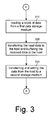
- a block of data is read from a first data storage medium (steps 310).
- the read data block is transferred to the host and buffered therein (step 320).
- the data write stage is started in step 330.
- the buffered data is transferred to the second data storage drive and written therein on a data storage media.
- the data is stored on both storage media in form of a plurality of data blocks which are individually copied between both drives.
- steps 310, 320 and 330 are performed in a repetitive manner in order to transfer all desired data.
- the process returns to step 310 after the execution of step 330 in order to start with the next block.
- Fig. 4 The sequence of the processing steps required for data copying with respect to time is shown in Fig. 4. After reading a first data block during time period 410, the obtained data is written to the second storage medium during time period 415. In a corresponding manner, the data of block 2 is read during time period 420 and written to a time period 425.
- the time period required for transferring a single data block from a first data storage drive to a second data storage drive corresponds to the accumulated of the read time period 410 and the write time period 415.
- Fig. 5 illustrates the timing diagram of a copy process in accordance with the present invention.
- the read and write operations which are conventionally performed subsequently are now performed in parallel.
- the data is transferred to the second data storage drive during a time period 512 and written thereon during a time period 514.
- the reading 510 of the data of the first block has been completed, the reading continues with the reading 512 of the data of the second block.
- the read and write procedures for each individual block are offset such that each block is written only after the data read procedure for the respective block has been completed.
- the parallel read and write operations are accomplished by employing a cache memory for buffering read data.
- the cache memory is located in the first data storage drive. Although a data transmission between the host and the connected drive is only possible to one of the data storage drives at a time, the read and write processes can be carried out concurrently.
- the read data are buffered within the first data storage drive 110, while the control unit or host 130 transfers the data from the cache memory of the first data storage drive to the second data storage drive which is instructed to write the received data on its storage medium.
- the drive can continuously read data to be stored therein. This can be achieved by employing a look-ahead functionality. This function already reads the next block of data and thus, enables an acceleration of the required read time 510.
- a particular optimization of the data exchange can be achieved when a data storage drive having a slow data access time is used as a first data storage drive, for instance a DVD drive, and a target drive having a short access time is used as the second data storage drive, for instance a hard disk drive.
- a data storage drive having a slow data access time is used as a first data storage drive, for instance a DVD drive
- a target drive having a short access time is used as the second data storage drive, for instance a hard disk drive.
- FIG. 6 the individual steps carried out during a data copying process in accordance with the present invention is illustrated.
- the processing blocks of Fig. 6 are arranged with respect to a time axis 600 in order to reflect the sequential and parallel relationships of the processing stages for subsequent data blocks.
- a block n is read from the first data storage drive and stored therein (step 612). After the reading and storing of block n is completed, a data transfer is requested by the control device and the stored data block is transferred accordingly to the host (step 614). The host then transmits the obtained data block to the target drive (step 614) while the first data storage drive already reads and stores data of a subsequent block n+1 (step 622).
- the data transmitted to the second data storage drive is written on the storage medium included therein (step 616).
- the reading and storing of data of block n + 1 may already completed before all data of the previous block n have been written to the second data storage drive. In such circumstances, small interruptions occur in the data reading process.
- the subsequent block n + 1 (which has already been read from the first data storage drive) is requested from the control device 130 and transferred thereto from the cache memory (steps 614, 624).
- the present invention accelerates a data transfer between two data storage drives by performing read and write operations in parallel. This is accomplished by buffering read data in a cache memory provided within the first data storage drive (source drive) while the data previously read are transferred and written to the second data storage drive (target drive).
Landscapes
- Engineering & Computer Science (AREA)
- Theoretical Computer Science (AREA)
- Human Computer Interaction (AREA)
- Physics & Mathematics (AREA)
- General Engineering & Computer Science (AREA)
- General Physics & Mathematics (AREA)
- Signal Processing For Digital Recording And Reproducing (AREA)
- Memory System Of A Hierarchy Structure (AREA)
- Communication Control (AREA)
Priority Applications (4)
| Application Number | Priority Date | Filing Date | Title |
|---|---|---|---|
| AT03021326T ATE345531T1 (de) | 2003-09-19 | 2003-09-19 | Ein verfahren zum datentransfer und eine datentransferschnittstelle |
| DE60309705T DE60309705T2 (de) | 2003-09-19 | 2003-09-19 | Ein Verfahren zum Datentransfer und eine Datentransferschnittstelle |
| EP03021326A EP1517246B1 (de) | 2003-09-19 | 2003-09-19 | Ein Verfahren zum Datentransfer und eine Datentransferschnittstelle |
| US10/944,130 US20050097268A1 (en) | 2003-09-19 | 2004-09-17 | System for transferring data from one storage device to another |
Applications Claiming Priority (1)
| Application Number | Priority Date | Filing Date | Title |
|---|---|---|---|
| EP03021326A EP1517246B1 (de) | 2003-09-19 | 2003-09-19 | Ein Verfahren zum Datentransfer und eine Datentransferschnittstelle |
Publications (2)
| Publication Number | Publication Date |
|---|---|
| EP1517246A1 true EP1517246A1 (de) | 2005-03-23 |
| EP1517246B1 EP1517246B1 (de) | 2006-11-15 |
Family
ID=34178460
Family Applications (1)
| Application Number | Title | Priority Date | Filing Date |
|---|---|---|---|
| EP03021326A Expired - Lifetime EP1517246B1 (de) | 2003-09-19 | 2003-09-19 | Ein Verfahren zum Datentransfer und eine Datentransferschnittstelle |
Country Status (4)
| Country | Link |
|---|---|
| US (1) | US20050097268A1 (de) |
| EP (1) | EP1517246B1 (de) |
| AT (1) | ATE345531T1 (de) |
| DE (1) | DE60309705T2 (de) |
Families Citing this family (6)
| Publication number | Priority date | Publication date | Assignee | Title |
|---|---|---|---|---|
| US7657615B1 (en) | 2002-12-08 | 2010-02-02 | Sun Microsystems, Inc. | Approach for provisioning network devices |
| US7237077B1 (en) * | 2002-12-08 | 2007-06-26 | Sun Microsystems, Inc. | Tool for disk image replication |
| US7917715B2 (en) * | 2006-01-28 | 2011-03-29 | Tallman Jr Leon C | Internet-safe computer |
| US9106721B2 (en) | 2012-10-02 | 2015-08-11 | Nextbit Systems | Application state synchronization across multiple devices |
| US9367258B2 (en) * | 2013-03-11 | 2016-06-14 | New Concepts Development Corp. | Systems and methods for managing storage space in hybrid data storage systems |
| US10105593B2 (en) * | 2014-04-08 | 2018-10-23 | Razer (Asia-Pacific) Pte. Ltd. | File prefetching for gaming applications accessed by electronic devices |
Citations (3)
| Publication number | Priority date | Publication date | Assignee | Title |
|---|---|---|---|---|
| US5446877A (en) * | 1990-11-13 | 1995-08-29 | Nakamichi Peripherals Corporation | Method and apparatus for operation of a data archival apparatus allowing for coupling of the data archival device with an ide interface |
| US5898891A (en) * | 1996-06-04 | 1999-04-27 | Micron Electronics, Inc. | Method for transferring data directly between the first and second data storage devices without transferring data to the memory array or over the input-output bus |
| US6301625B1 (en) * | 1997-11-14 | 2001-10-09 | 3Ware, Inc. | System and method for processing and tracking the completion of I/O requests in a disk array system |
Family Cites Families (6)
| Publication number | Priority date | Publication date | Assignee | Title |
|---|---|---|---|---|
| US5968147A (en) * | 1997-09-26 | 1999-10-19 | Adaptec, Inc. | Method and apparatus for improved peripheral bus utilization |
| US6791907B2 (en) * | 1999-04-22 | 2004-09-14 | Roxio, Inc. | Automobile audio system for collection, management and playback of audio data |
| JP2001165671A (ja) * | 1999-12-14 | 2001-06-22 | Pioneer Electronic Corp | ナビゲーションシステム |
| US6658525B1 (en) * | 2000-09-28 | 2003-12-02 | International Business Machines Corporation | Concurrent access of an unsegmented buffer by writers and readers of the buffer |
| TW548923B (en) * | 2001-06-12 | 2003-08-21 | Realtek Semiconductor Corp | Data register in communication system and method thereof |
| US20040250039A1 (en) * | 2003-06-05 | 2004-12-09 | Hanks D. Mitchel | System and method for using swappable storage for high data content multi-source data storage |
-
2003
- 2003-09-19 AT AT03021326T patent/ATE345531T1/de not_active IP Right Cessation
- 2003-09-19 DE DE60309705T patent/DE60309705T2/de not_active Expired - Lifetime
- 2003-09-19 EP EP03021326A patent/EP1517246B1/de not_active Expired - Lifetime
-
2004
- 2004-09-17 US US10/944,130 patent/US20050097268A1/en not_active Abandoned
Patent Citations (3)
| Publication number | Priority date | Publication date | Assignee | Title |
|---|---|---|---|---|
| US5446877A (en) * | 1990-11-13 | 1995-08-29 | Nakamichi Peripherals Corporation | Method and apparatus for operation of a data archival apparatus allowing for coupling of the data archival device with an ide interface |
| US5898891A (en) * | 1996-06-04 | 1999-04-27 | Micron Electronics, Inc. | Method for transferring data directly between the first and second data storage devices without transferring data to the memory array or over the input-output bus |
| US6301625B1 (en) * | 1997-11-14 | 2001-10-09 | 3Ware, Inc. | System and method for processing and tracking the completion of I/O requests in a disk array system |
Also Published As
| Publication number | Publication date |
|---|---|
| DE60309705T2 (de) | 2007-03-29 |
| US20050097268A1 (en) | 2005-05-05 |
| EP1517246B1 (de) | 2006-11-15 |
| DE60309705D1 (de) | 2006-12-28 |
| ATE345531T1 (de) | 2006-12-15 |
Similar Documents
| Publication | Publication Date | Title |
|---|---|---|
| US4905184A (en) | Address control system for segmented buffer memory | |
| US20020178331A1 (en) | Prestaging data into cache in preparation for data transfer operations | |
| JPH0793219A (ja) | 情報処理装置 | |
| US6292878B1 (en) | Data recorder and method of access to data recorder | |
| CN103226525B (zh) | 存储器装置、计算装置和数据传输方法 | |
| EP1517247A1 (de) | Datenübertragungsschnittstelle | |
| EP1517246B1 (de) | Ein Verfahren zum Datentransfer und eine Datentransferschnittstelle | |
| KR20060017816A (ko) | 주 메모리와 기억 장치 사이에서 데이터를 전송하는 방법및 장치 | |
| US8386725B2 (en) | USB host controller and controlling method for USB host controller | |
| US20040128457A1 (en) | Disk drive with copy function | |
| JP2007102436A (ja) | ストレージ制御装置およびストレージ制御方法 | |
| US7424556B1 (en) | Method and system for sharing a receive buffer RAM with a single DMA engine among multiple context engines | |
| KR920007949B1 (ko) | 컴퓨터 주변장치 제어기 | |
| JPH09128159A (ja) | 記憶装置 | |
| JP2007058816A (ja) | データ記録再生装置及びその制御方法 | |
| JP2001209577A (ja) | 情報記録再生装置 | |
| JP2000306389A (ja) | 不揮発性半導体メモリを用いた記憶装置 | |
| JPH08297917A (ja) | データコピーシステム | |
| US7957229B2 (en) | Optical disc controller and optical disc drive system using error correction codes | |
| JPH08195030A (ja) | ディスク装置のデータ転送方法 | |
| JPS63213018A (ja) | 外部記憶制御装置 | |
| JPH04255960A (ja) | ディスクドライブ並列操作方法 | |
| JP3524954B2 (ja) | ディスク制御装置 | |
| JPH08106363A (ja) | マルチディスク装置 | |
| JP2001222381A (ja) | パーシャルライト処理を行うディスク制御装置、ディスクサブシステム、ディスク制御装置の制御方法、及びプログラムを記録した記録媒体。 |
Legal Events
| Date | Code | Title | Description |
|---|---|---|---|
| PUAI | Public reference made under article 153(3) epc to a published international application that has entered the european phase |
Free format text: ORIGINAL CODE: 0009012 |
|
| AK | Designated contracting states |
Kind code of ref document: A1 Designated state(s): AT BE BG CH CY CZ DE DK EE ES FI FR GB GR HU IE IT LI LU MC NL PT RO SE SI SK TR |
|
| AX | Request for extension of the european patent |
Extension state: AL LT LV MK |
|
| 17P | Request for examination filed |
Effective date: 20050923 |
|
| AKX | Designation fees paid |
Designated state(s): AT BE BG CH CY CZ DE DK EE ES FI FR GB GR HU IE IT LI LU MC NL PT RO SE SI SK TR |
|
| GRAP | Despatch of communication of intention to grant a patent |
Free format text: ORIGINAL CODE: EPIDOSNIGR1 |
|
| GRAS | Grant fee paid |
Free format text: ORIGINAL CODE: EPIDOSNIGR3 |
|
| GRAA | (expected) grant |
Free format text: ORIGINAL CODE: 0009210 |
|
| AK | Designated contracting states |
Kind code of ref document: B1 Designated state(s): AT BE BG CH CY CZ DE DK EE ES FI FR GB GR HU IE IT LI LU MC NL PT RO SE SI SK TR |
|
| PG25 | Lapsed in a contracting state [announced via postgrant information from national office to epo] |
Ref country code: LI Free format text: LAPSE BECAUSE OF FAILURE TO SUBMIT A TRANSLATION OF THE DESCRIPTION OR TO PAY THE FEE WITHIN THE PRESCRIBED TIME-LIMIT Effective date: 20061115 Ref country code: FI Free format text: LAPSE BECAUSE OF FAILURE TO SUBMIT A TRANSLATION OF THE DESCRIPTION OR TO PAY THE FEE WITHIN THE PRESCRIBED TIME-LIMIT Effective date: 20061115 Ref country code: AT Free format text: LAPSE BECAUSE OF FAILURE TO SUBMIT A TRANSLATION OF THE DESCRIPTION OR TO PAY THE FEE WITHIN THE PRESCRIBED TIME-LIMIT Effective date: 20061115 Ref country code: IT Free format text: LAPSE BECAUSE OF FAILURE TO SUBMIT A TRANSLATION OF THE DESCRIPTION OR TO PAY THE FEE WITHIN THE PRESCRIBED TIME-LIMIT;WARNING: LAPSES OF ITALIAN PATENTS WITH EFFECTIVE DATE BEFORE 2007 MAY HAVE OCCURRED AT ANY TIME BEFORE 2007. THE CORRECT EFFECTIVE DATE MAY BE DIFFERENT FROM THE ONE RECORDED. Effective date: 20061115 Ref country code: RO Free format text: LAPSE BECAUSE OF FAILURE TO SUBMIT A TRANSLATION OF THE DESCRIPTION OR TO PAY THE FEE WITHIN THE PRESCRIBED TIME-LIMIT Effective date: 20061115 Ref country code: CZ Free format text: LAPSE BECAUSE OF FAILURE TO SUBMIT A TRANSLATION OF THE DESCRIPTION OR TO PAY THE FEE WITHIN THE PRESCRIBED TIME-LIMIT Effective date: 20061115 Ref country code: CH Free format text: LAPSE BECAUSE OF FAILURE TO SUBMIT A TRANSLATION OF THE DESCRIPTION OR TO PAY THE FEE WITHIN THE PRESCRIBED TIME-LIMIT Effective date: 20061115 Ref country code: SI Free format text: LAPSE BECAUSE OF FAILURE TO SUBMIT A TRANSLATION OF THE DESCRIPTION OR TO PAY THE FEE WITHIN THE PRESCRIBED TIME-LIMIT Effective date: 20061115 Ref country code: SK Free format text: LAPSE BECAUSE OF FAILURE TO SUBMIT A TRANSLATION OF THE DESCRIPTION OR TO PAY THE FEE WITHIN THE PRESCRIBED TIME-LIMIT Effective date: 20061115 Ref country code: NL Free format text: LAPSE BECAUSE OF FAILURE TO SUBMIT A TRANSLATION OF THE DESCRIPTION OR TO PAY THE FEE WITHIN THE PRESCRIBED TIME-LIMIT Effective date: 20061115 Ref country code: BE Free format text: LAPSE BECAUSE OF FAILURE TO SUBMIT A TRANSLATION OF THE DESCRIPTION OR TO PAY THE FEE WITHIN THE PRESCRIBED TIME-LIMIT Effective date: 20061115 |
|
| REG | Reference to a national code |
Ref country code: GB Ref legal event code: FG4D |
|
| REG | Reference to a national code |
Ref country code: CH Ref legal event code: EP |
|
| REF | Corresponds to: |
Ref document number: 60309705 Country of ref document: DE Date of ref document: 20061228 Kind code of ref document: P |
|
| REG | Reference to a national code |
Ref country code: IE Ref legal event code: FG4D |
|
| PG25 | Lapsed in a contracting state [announced via postgrant information from national office to epo] |
Ref country code: DK Free format text: LAPSE BECAUSE OF FAILURE TO SUBMIT A TRANSLATION OF THE DESCRIPTION OR TO PAY THE FEE WITHIN THE PRESCRIBED TIME-LIMIT Effective date: 20070215 Ref country code: BG Free format text: LAPSE BECAUSE OF FAILURE TO SUBMIT A TRANSLATION OF THE DESCRIPTION OR TO PAY THE FEE WITHIN THE PRESCRIBED TIME-LIMIT Effective date: 20070215 Ref country code: SE Free format text: LAPSE BECAUSE OF FAILURE TO SUBMIT A TRANSLATION OF THE DESCRIPTION OR TO PAY THE FEE WITHIN THE PRESCRIBED TIME-LIMIT Effective date: 20070215 |
|
| PG25 | Lapsed in a contracting state [announced via postgrant information from national office to epo] |
Ref country code: ES Free format text: LAPSE BECAUSE OF FAILURE TO SUBMIT A TRANSLATION OF THE DESCRIPTION OR TO PAY THE FEE WITHIN THE PRESCRIBED TIME-LIMIT Effective date: 20070226 |
|
| PG25 | Lapsed in a contracting state [announced via postgrant information from national office to epo] |
Ref country code: PT Free format text: LAPSE BECAUSE OF FAILURE TO SUBMIT A TRANSLATION OF THE DESCRIPTION OR TO PAY THE FEE WITHIN THE PRESCRIBED TIME-LIMIT Effective date: 20070416 |
|
| ET | Fr: translation filed | ||
| NLV1 | Nl: lapsed or annulled due to failure to fulfill the requirements of art. 29p and 29m of the patents act | ||
| REG | Reference to a national code |
Ref country code: CH Ref legal event code: PL |
|
| PLBE | No opposition filed within time limit |
Free format text: ORIGINAL CODE: 0009261 |
|
| STAA | Information on the status of an ep patent application or granted ep patent |
Free format text: STATUS: NO OPPOSITION FILED WITHIN TIME LIMIT |
|
| 26N | No opposition filed |
Effective date: 20070817 |
|
| PG25 | Lapsed in a contracting state [announced via postgrant information from national office to epo] |
Ref country code: MC Free format text: LAPSE BECAUSE OF NON-PAYMENT OF DUE FEES Effective date: 20070930 Ref country code: GR Free format text: LAPSE BECAUSE OF FAILURE TO SUBMIT A TRANSLATION OF THE DESCRIPTION OR TO PAY THE FEE WITHIN THE PRESCRIBED TIME-LIMIT Effective date: 20070216 |
|
| PG25 | Lapsed in a contracting state [announced via postgrant information from national office to epo] |
Ref country code: IE Free format text: LAPSE BECAUSE OF NON-PAYMENT OF DUE FEES Effective date: 20070919 |
|
| PG25 | Lapsed in a contracting state [announced via postgrant information from national office to epo] |
Ref country code: EE Free format text: LAPSE BECAUSE OF FAILURE TO SUBMIT A TRANSLATION OF THE DESCRIPTION OR TO PAY THE FEE WITHIN THE PRESCRIBED TIME-LIMIT Effective date: 20061115 |
|
| PG25 | Lapsed in a contracting state [announced via postgrant information from national office to epo] |
Ref country code: CY Free format text: LAPSE BECAUSE OF FAILURE TO SUBMIT A TRANSLATION OF THE DESCRIPTION OR TO PAY THE FEE WITHIN THE PRESCRIBED TIME-LIMIT Effective date: 20061115 Ref country code: LU Free format text: LAPSE BECAUSE OF NON-PAYMENT OF DUE FEES Effective date: 20070919 |
|
| PG25 | Lapsed in a contracting state [announced via postgrant information from national office to epo] |
Ref country code: TR Free format text: LAPSE BECAUSE OF FAILURE TO SUBMIT A TRANSLATION OF THE DESCRIPTION OR TO PAY THE FEE WITHIN THE PRESCRIBED TIME-LIMIT Effective date: 20061115 Ref country code: HU Free format text: LAPSE BECAUSE OF FAILURE TO SUBMIT A TRANSLATION OF THE DESCRIPTION OR TO PAY THE FEE WITHIN THE PRESCRIBED TIME-LIMIT Effective date: 20070516 |
|
| PGFP | Annual fee paid to national office [announced via postgrant information from national office to epo] |
Ref country code: GB Payment date: 20130927 Year of fee payment: 11 Ref country code: FR Payment date: 20130919 Year of fee payment: 11 |
|
| PGFP | Annual fee paid to national office [announced via postgrant information from national office to epo] |
Ref country code: IT Payment date: 20130924 Year of fee payment: 11 |
|
| GBPC | Gb: european patent ceased through non-payment of renewal fee |
Effective date: 20140919 |
|
| REG | Reference to a national code |
Ref country code: FR Ref legal event code: ST Effective date: 20150529 |
|
| PG25 | Lapsed in a contracting state [announced via postgrant information from national office to epo] |
Ref country code: GB Free format text: LAPSE BECAUSE OF NON-PAYMENT OF DUE FEES Effective date: 20140919 |
|
| PG25 | Lapsed in a contracting state [announced via postgrant information from national office to epo] |
Ref country code: IT Free format text: LAPSE BECAUSE OF NON-PAYMENT OF DUE FEES Effective date: 20140919 Ref country code: FR Free format text: LAPSE BECAUSE OF NON-PAYMENT OF DUE FEES Effective date: 20140930 |
|
| REG | Reference to a national code |
Ref country code: DE Ref legal event code: R082 Ref document number: 60309705 Country of ref document: DE Representative=s name: MAUCHER JENKINS PATENTANWAELTE & RECHTSANWAELT, DE |
|
| PGFP | Annual fee paid to national office [announced via postgrant information from national office to epo] |
Ref country code: DE Payment date: 20220616 Year of fee payment: 20 |
|
| P01 | Opt-out of the competence of the unified patent court (upc) registered |
Effective date: 20230526 |
|
| REG | Reference to a national code |
Ref country code: DE Ref legal event code: R071 Ref document number: 60309705 Country of ref document: DE |