EP1517177A2 - Method of producing a pattern and photomask used in the same - Google Patents
Method of producing a pattern and photomask used in the same Download PDFInfo
- Publication number
- EP1517177A2 EP1517177A2 EP04030778A EP04030778A EP1517177A2 EP 1517177 A2 EP1517177 A2 EP 1517177A2 EP 04030778 A EP04030778 A EP 04030778A EP 04030778 A EP04030778 A EP 04030778A EP 1517177 A2 EP1517177 A2 EP 1517177A2
- Authority
- EP
- European Patent Office
- Prior art keywords
- layer
- photocatalyst
- pattern
- characteristic
- modifiable
- Prior art date
- Legal status (The legal status is an assumption and is not a legal conclusion. Google has not performed a legal analysis and makes no representation as to the accuracy of the status listed.)
- Withdrawn
Links
Images


Classifications
-
- G—PHYSICS
- G03—PHOTOGRAPHY; CINEMATOGRAPHY; ANALOGOUS TECHNIQUES USING WAVES OTHER THAN OPTICAL WAVES; ELECTROGRAPHY; HOLOGRAPHY
- G03F—PHOTOMECHANICAL PRODUCTION OF TEXTURED OR PATTERNED SURFACES, e.g. FOR PRINTING, FOR PROCESSING OF SEMICONDUCTOR DEVICES; MATERIALS THEREFOR; ORIGINALS THEREFOR; APPARATUS SPECIALLY ADAPTED THEREFOR
- G03F1/00—Originals for photomechanical production of textured or patterned surfaces, e.g., masks, photo-masks, reticles; Mask blanks or pellicles therefor; Containers specially adapted therefor; Preparation thereof
- G03F1/38—Masks having auxiliary features, e.g. special coatings or marks for alignment or testing; Preparation thereof
-
- G—PHYSICS
- G03—PHOTOGRAPHY; CINEMATOGRAPHY; ANALOGOUS TECHNIQUES USING WAVES OTHER THAN OPTICAL WAVES; ELECTROGRAPHY; HOLOGRAPHY
- G03F—PHOTOMECHANICAL PRODUCTION OF TEXTURED OR PATTERNED SURFACES, e.g. FOR PRINTING, FOR PROCESSING OF SEMICONDUCTOR DEVICES; MATERIALS THEREFOR; ORIGINALS THEREFOR; APPARATUS SPECIALLY ADAPTED THEREFOR
- G03F7/00—Photomechanical, e.g. photolithographic, production of textured or patterned surfaces, e.g. printing surfaces; Materials therefor, e.g. comprising photoresists; Apparatus specially adapted therefor
- G03F7/0005—Production of optical devices or components in so far as characterised by the lithographic processes or materials used therefor
- G03F7/0007—Filters, e.g. additive colour filters; Components for display devices
-
- B—PERFORMING OPERATIONS; TRANSPORTING
- B82—NANOTECHNOLOGY
- B82Y—SPECIFIC USES OR APPLICATIONS OF NANOSTRUCTURES; MEASUREMENT OR ANALYSIS OF NANOSTRUCTURES; MANUFACTURE OR TREATMENT OF NANOSTRUCTURES
- B82Y30/00—Nanotechnology for materials or surface science, e.g. nanocomposites
-
- G—PHYSICS
- G03—PHOTOGRAPHY; CINEMATOGRAPHY; ANALOGOUS TECHNIQUES USING WAVES OTHER THAN OPTICAL WAVES; ELECTROGRAPHY; HOLOGRAPHY
- G03F—PHOTOMECHANICAL PRODUCTION OF TEXTURED OR PATTERNED SURFACES, e.g. FOR PRINTING, FOR PROCESSING OF SEMICONDUCTOR DEVICES; MATERIALS THEREFOR; ORIGINALS THEREFOR; APPARATUS SPECIALLY ADAPTED THEREFOR
- G03F1/00—Originals for photomechanical production of textured or patterned surfaces, e.g., masks, photo-masks, reticles; Mask blanks or pellicles therefor; Containers specially adapted therefor; Preparation thereof
- G03F1/62—Pellicles, e.g. pellicle assemblies, e.g. having membrane on support frame; Preparation thereof
-
- G—PHYSICS
- G03—PHOTOGRAPHY; CINEMATOGRAPHY; ANALOGOUS TECHNIQUES USING WAVES OTHER THAN OPTICAL WAVES; ELECTROGRAPHY; HOLOGRAPHY
- G03F—PHOTOMECHANICAL PRODUCTION OF TEXTURED OR PATTERNED SURFACES, e.g. FOR PRINTING, FOR PROCESSING OF SEMICONDUCTOR DEVICES; MATERIALS THEREFOR; ORIGINALS THEREFOR; APPARATUS SPECIALLY ADAPTED THEREFOR
- G03F7/00—Photomechanical, e.g. photolithographic, production of textured or patterned surfaces, e.g. printing surfaces; Materials therefor, e.g. comprising photoresists; Apparatus specially adapted therefor
- G03F7/0005—Production of optical devices or components in so far as characterised by the lithographic processes or materials used therefor
- G03F7/001—Phase modulating patterns, e.g. refractive index patterns
-
- G—PHYSICS
- G03—PHOTOGRAPHY; CINEMATOGRAPHY; ANALOGOUS TECHNIQUES USING WAVES OTHER THAN OPTICAL WAVES; ELECTROGRAPHY; HOLOGRAPHY
- G03F—PHOTOMECHANICAL PRODUCTION OF TEXTURED OR PATTERNED SURFACES, e.g. FOR PRINTING, FOR PROCESSING OF SEMICONDUCTOR DEVICES; MATERIALS THEREFOR; ORIGINALS THEREFOR; APPARATUS SPECIALLY ADAPTED THEREFOR
- G03F7/00—Photomechanical, e.g. photolithographic, production of textured or patterned surfaces, e.g. printing surfaces; Materials therefor, e.g. comprising photoresists; Apparatus specially adapted therefor
- G03F7/004—Photosensitive materials
- G03F7/09—Photosensitive materials characterised by structural details, e.g. supports, auxiliary layers
- G03F7/11—Photosensitive materials characterised by structural details, e.g. supports, auxiliary layers having cover layers or intermediate layers, e.g. subbing layers
-
- G—PHYSICS
- G03—PHOTOGRAPHY; CINEMATOGRAPHY; ANALOGOUS TECHNIQUES USING WAVES OTHER THAN OPTICAL WAVES; ELECTROGRAPHY; HOLOGRAPHY
- G03F—PHOTOMECHANICAL PRODUCTION OF TEXTURED OR PATTERNED SURFACES, e.g. FOR PRINTING, FOR PROCESSING OF SEMICONDUCTOR DEVICES; MATERIALS THEREFOR; ORIGINALS THEREFOR; APPARATUS SPECIALLY ADAPTED THEREFOR
- G03F7/00—Photomechanical, e.g. photolithographic, production of textured or patterned surfaces, e.g. printing surfaces; Materials therefor, e.g. comprising photoresists; Apparatus specially adapted therefor
- G03F7/20—Exposure; Apparatus therefor
- G03F7/2002—Exposure; Apparatus therefor with visible light or UV light, through an original having an opaque pattern on a transparent support, e.g. film printing, projection printing; by reflection of visible or UV light from an original such as a printed image
- G03F7/2014—Contact or film exposure of light sensitive plates such as lithographic plates or circuit boards, e.g. in a vacuum frame
-
- Y—GENERAL TAGGING OF NEW TECHNOLOGICAL DEVELOPMENTS; GENERAL TAGGING OF CROSS-SECTIONAL TECHNOLOGIES SPANNING OVER SEVERAL SECTIONS OF THE IPC; TECHNICAL SUBJECTS COVERED BY FORMER USPC CROSS-REFERENCE ART COLLECTIONS [XRACs] AND DIGESTS
- Y10—TECHNICAL SUBJECTS COVERED BY FORMER USPC
- Y10S—TECHNICAL SUBJECTS COVERED BY FORMER USPC CROSS-REFERENCE ART COLLECTIONS [XRACs] AND DIGESTS
- Y10S430/00—Radiation imagery chemistry: process, composition, or product thereof
- Y10S430/148—Light sensitive titanium compound containing
Definitions
- the present invention relates to a method of producing a pattern-formed structure, which structure is less likely to deteriorate as time elapses after the characteristic thereof is modified by using a photocatalyst, because no pyotocatalyst exists in the resulting pattern-formed structure.
- the present invention also relates to a photomask which can be used in the aforementioned method of producing a pattern-formed structure.
- a method of producing a pattern-formed structure by photolithography such as a method which includes the processes of: carrying out pattern-exposure of a photoresist layer provided by coating on a base material; developing the photoresist after the exposure; and effecting etching of the developed photoresist layer, and a method which includes the processes of: employing a functional substance as the photoresist; and directly forming the aimed pattern by exposure of the photoresist.
- the inventors of the present invention and other researchers have studied a method of producing a pat tern-formed structure in which method a pattern is formed by using a substance whose wetting property is modified by the action of a photocatalyst.
- the produced pattern-formed structure itself structurally includes the photocatalyst therein, whereby, depending the type of the pattern-formed structure, a problem arises in that the product may deteriorate due to the photocatalyst contained therein.
- the present invention is provided in order to solve the above-described problems.
- the main object of the present invention is to provide a method of producing a pattern-formed structure, in which method a highly precise pattern formation is possible in production of a pattern-formed structure, no post-exposure treatment is required and no photocatalyst is contained inside the produced pattern-formed structure, whereby there is no concern that the obtained pattern-formed structure deteriorates.
- a method of producing a pattern-formed structure comprises the processes of: preparing a substrate for a pattern-formed structure having a characteristic-modifiable layer whose characteristic at a surface thereof can be modified by the action of photocatalyst; arranging the substrate for a pattern-formed structure and a photocatalyst-containing-layer side substrate having a photocatalyst-containing layer formed on a base material, the photocatalyst-containing layer containing photocatalyst, such that the characteristic-modifiable layer faces the photocatalyst-containing layer with a gap of no larger than 200 ⁇ m therebetween; and irradiating energy to the characteristic-modifiable layer from a predetermined direction, and modifying characteristic of a surface of the characteristic-modifiable layer, thereby forming a pattern at the characteristic-modifiable layer.
- a pattern having various properties can be formed in a highly precise manner, without necessity of any specific treatment after irradiation of energy. Further, as the photocatalyst-containing-layer side substrate is removed form the pattern-formed structure after irradiation of energy, the pattern-formed structure itself includes no photocatalyst-containing layer, whereby there is no possibility that the pattern-formed structure deteriorates as time elapses by the action of the photocatalyst.
- the gap or space between the photocatalyst-containing layer and the characteristic-modifiable layer is set within the above-described range, a pattern-formed structure having a pattern produced as a result of modification of characteristic thereof can be obtained in an efficient and highly precise manner.
- the photocatalyst-containing layer and the characteristic-modifiable layer are preferably disposed such that the gap therebetween is in a range of 0.2 to 10 ⁇ m.
- the gap between the photocatalyst-containing layer and the characteristic-modifiable layer is set in a range of 0.2 to 10 ⁇ m, a pattern-formed structure having a pattern produced as a result of modification of characteristic thereof can be obtained by irradiation of energy in a relatively short time.
- the photocatalyst-containing-layer side substrate is preferably constituted of the base material and a photocatalyst-containing layer formed, in a pattern-like configuration, on the base material.
- a pattern having a different characteristic can be formed on the characteristic-modifiable layer, without using a photomask.
- the type of energy to be irradiated is not particularly restricted to energy provided in parallel and the direction of irradiating energy is not particularly restricted, either. Accordingly, in this appect, the degree of freedom in the types of the energy source and the arrangement thereof is significantly increased, which advantageous.
- the photocatalyst-containing-layer side substrate is constituted of the base material, the photocatalyst-containing layer formed on the base material, and a light-shielding portion formed in a pattern-like configuration, and the irradiation of energy at the aforementioned pattern forming process is carried out from the photocatalyst-containing-layer side substrate.
- Providing the light-shielding portion in the photocatalyst-containing-layer side substrate as described above renders use of a photomask or the like during energy irradiation obsolete. Accordingly, the process of aligning the photocatalyst-containing-layer side substrate with a photomask, or the like, is no longer required, contributing to simplifying the whole production processes.
- the light-shielding portion is formed, in a pattern-configuration, on the base material and the photocatalyst-containing layer is formed on the light-shielding portion.
- the photocatalyst-containing layer is formed on the base material and the light-shielding portion is formed, in a pattern-configuration, on the photocatalyst-containing layer.
- the light-shielding portion is disposed at a position close to the characteristic-modifiable layer, in terms of enhancing precision of the resulting characteristic pattern. Therefore, it is preferable that the light-shielding portion is disposed at the above-described position. Further, in a case in which the light-shielding portion is provided on the photocatalyst-containing layer, the light-shielding portion can serve as a spacer when the photocatalyst-containing layer is disposed with respect to the characteristic-modifiable layer in the aforementioned pattern forming process, which is advantageous.
- a spacer having thickness in a range of 0.2 to 10 ⁇ m is formed, in a patter-like configuration, on the photocatalyst-containing layer and exposure is effected in a state in which the spacer is in contact with the characteristic-modifiable layer.
- a spacer is provided in a pattern-like configuration on the photocatalyst-containing layer and exposure is effected in a state in which the spacer is in contact with the characteristic-modifiable layer.
- the distance between the photocatalyst-containing layer and the characteristic-modifiable layer can be easily kept in a range of 0.2 to 10 ⁇ m.
- these portions do not cause any modification to the corresponding portions of the characteristic-modifiable layer upon irradiation of energy. Accordingly, the same pattern as that of the spacer can be formed on the characteristic-modifiable layer as a result of the characteristic modification thereof.
- the spacer is preferably a light-shielding portion made of a light-shielding material.
- the spacer serves as a light-shielding portion, a highly precise pattern can be formed by effecting irradiation of energy in a state in which the light-shielding portion is in close contact with the characteristic-modifiable layer.
- the present invention also provides a method of producing a pattern-formed structure, comprising the processes of: preparing a photocatalyst-containing-layer side substrate in which a photocatalyst-containing layer is formed on a photomask by way of a primer layer, the photomask being formed by providing a light-shielding portion, in a pattern-like configuration, on a transparent base material; preparing a substrate for a pattern-formed structure having a characteristic-modifiable layer whose characteristic can be modified by the action of photocatalyst contained at least in the photocatalyst-containing layer; arranging the photocatalyst-containing-layer side substrate and the substrate for a pattern-formed structure: such that the photocatalyst-containing layer and the substrate for a pattern-formed structure are in contact with each other; or such that the characteristic-modifiable layer faces the photocatalyst-containing layer with a gap therebetween, the gap being narrow enough to allow the action of the photocatalys
- a pattern can be produced with high sensitivity and in a highly precise manner, without necessity of carrying out any specific treatment after irradiation of energy.
- the characteristic-modifiable-layer side substrate itself does not include any photocatalyst-containing layer. Therefore, there arises no concern that the characteristic-modifiable-layer side substrate deteriorates as time elapses by the action of the photocatalyst.
- the residuals or the like generated at the light-shielding portion at the time of patterning and existing thereafter at the light-shielding portion or the opening portion between one light-shielding portion and the other do not affect the action of the photocatalyst, as a result of the excellent effect of the primer layer. Accordingly, the sensitivity of the photocatalyst can be enhanced and a pattern, produced as a result of modification of characteristic, can be obtained even by irradiation of energy in a relatively short time.
- the gap which is narrow enough to allow the action of the photocatalyst of the photocatalyst-containing layer to effect on the characteristic-modifiable layer is in a range of 0.2 to 10 ⁇ m.
- the gap between the photocatalyst-containing layer and the characteristic-modifiable layer is in a range of 0.2 to 10 ⁇ m, a pattern-formed body having a pattern produced as a result of modification of characteristic thereof can be obtained by irradiation of energy in a relatively short time.
- the photocatalyst-containing layer is a layer made of photocatalyst.
- the photocatalyst-containing layer is made of only photocatalyst, the efficiency at which the characteristic of the characteristic-modifiable layer is modified can be enhanced, whereby a pattern-formed structure can be efficiently produced.
- the photocatalyst-containing layer is a layer formed by providing a photocatalyst in a formof a film on a base material by a vacuum film making method.
- a photocatalyst-containing layer having constant film thickness and less irregularities at the surface thereof can be produced, whereby formation of the characteristic pattern at the characteristic-modifiable layer surface can be performed evenly and in a higly efficient manner.
- the photocatalyst-containing layer is a layer containing a photocatalyst and a binder.
- a binder in such a manner, the photocatalyst-containing layer can be formed relatively easily, whereby a pattern-formed structure can be produced at a low cost.
- the photocatalyst is at least one type of compound selected from the group consisting of titanium oxide (TiO 2 ), zinc oxide (ZnO), tin oxide (SnO 2 ), strontium titanate (SrTiO 3 ), tungsten oxide (WO 3 ), bismuth oxide (Bi 2 O 3 ) and iron oxide (Fe 2 O 3 ).
- the photocatalyst is titanium oxide (TiO 2 ). Titanium dioxide, having high band gap energy, acts effectively as a photocatalyst, is chemically stable, has no toxicity, and is easily available.
- the substrate for a pattern-formed structure is constituted, at least, of a substrate and the characteristic-modifiable layer provided on said substrate.
- a characteristic-modifiable layer generally has various characteristics, it is preferable that the characteristic-modifiable layer is formed as a thin film on the substrate, in terms of strength, cost efficiency and functional aspects.
- the characteristic-modifiable layer is a wetting-property-modifiable layer whose wetting property can be modified, such that a contact angle formed by a liquid on said wetting-property-modifiable layer is decreased upon irradiation of energy by the action of the photocatalyst in the photocatalyst-containing layer.
- the characteristic of the characteristic-modifiable layer include various characteristics, and one important example thereof is the change in the wetting property.
- the characteristic-modifiable layer as a wetting-property-modifiable layer
- a pattern-formed structure having a pattern produced as a result of modification of the wetting-property thereof by the action of the photocatalyst can be obtained.
- various types of functional elements including a color filter and a microlens, can be formed as described below.
- the contact angle formed on said wetting-property-modifiable layer by a liquid whose surface tension is 40 mN/m is no smaller than 10° at an unexposed portion of the layer and no larger than 9° at an exposed portion.
- the portion which is not subjected to energy irradiation is a portion which is required to exhibit liquid-repellency and the portion which is subjected to energy irradiation is a portion which is required to exhibit lyophilicity. Therefore,thewetting property as described above is necessary in the wetting-property-modifiable layer.
- said wetting-property-modifiable layer is a layer containing organopolysiloxane.
- the organopolysiloxane is a polysiloxane containing the fluoroalkyl group.
- a wetting-property-modifiable layer can exhibit a large magnitude of change in the wetting property when energy is irradiated in a state in which the photocatalyst-containing layer is in contact therewith.
- the organopolysiloxane is an organopolysiloxane obtained as a result of hydrolysis condensation or cohydrolysis condensation of at least one type of silicon compound generally represented by a formula Y n SiX (4-n) , wherein Y represents a group selected from the group consisting of the alkyl group, the fluoroalkyl group, the vinyl group, the amino group, the phenyl group and the epoxy group, X represents the alkoxyl group or the halogen group, and n represents an integer of 0 to 3.
- the substrate for a pattern-formed structure is a self-supporting film, and at least one surface thereof is a film-like wetting-property-modifiable layer whose wetting property can be modified, such that a contact angle formed by a liquid on said wetting-property-modifiable layer is decreased upon irradiation of energy, by the action of the photocatalyst in the photocatalyst-containing layer.
- a pattern having different wetting characteristic can be obtained simply by effecting energy irradiation in a state in which one surface of a commercially available film, made of a predetermined material, is in contact with the photocatalyst-containing layer, which is advantageous in terms of cost reduction.
- the characteristic-modifiable layer is a decomposable and removable layer which is decomposed and removed by the action of the photocatalyst contained in the photocatalyst-containing layer.
- the characteristic-modifiable layer is a decomposable and removable layer which is decomposed and removed by the action of the photocatalyst contained in the photocatalyst-containing layer.
- the decomposable and removable layer as a photoresist and effecting exposure in a state in which the decomposable and removable layer is in contact with the photocatalyst-containing-layer side substrate, a pattern can be formed at the photoresist without necessityof carrying out the conventional development process.
- Other applications of various types are also possible in the structure of the present aspect.
- a contact angle formed by a liquid on the decomposable and removable layer is different from a contact angle formed by the liquid on the substrate which has been exposed as a result of decomposition and removal of the decomposable and removable layer.
- the base material is exposed at the surface as a result of decomposition and removal of the decomposable and removable layer by the action of the photocatalyst.
- the decomposable and removable layer remains at the portion which is not been subjected to energy irradiation.
- the decomposable and removable layer is made of a material having liquid repellency and the base material is made of a material having excellent affinity with a liquid (lyophilicity), for example, a portion of the decomposable and removable layer, at which portion a functional portion is to be formed, can be removed by irradiating energy in advance to the portion and thereby causing the photocatalyst to effect thereon.
- the energy-irradiated portion becomes a recessed portion which serves as an area having excellent lyophilicity, while the portion which is not subjected to energy irradiation becomes a projected portion which serves as a liquid-repellent area. Accordingly, the composition for the functional portion can be attached, easily and precisely, to the recessed portion in which the functional portion is to be provided and which serves as the area having excellent lyophilicity.
- the functional portion can be formed more precisely than the aforementioned case in which the characteristic-modifiable layer is a wetting-property-modifiable layer and there is no necessity of carrying out the post-treatment such as the developing or washing process after irradiation of energy. Therefore, the production process as a whole can be easily rendered a simpler state, whereby a functional element which is cheap and has a highly precise functional portion can be obtained.
- the decomposable and removable layer is selected from the group consisting of a Self-Assembled Monolayer Film, a Langmuir-Blodgett's Film and a Layer-by-Layer Self-Assembled Film. These materials are decomposed and removed by the action of the photocatalys contained in the photocatalyst-containing layer, so as to effect various functions.
- the irradiation of energy is carried out when the photocatalyst-containing layer is being heated.
- the sensitivity of the photocatalys is enhanced, whereby modification of the characteristic at the characteristic-modifiable layer can be efficiently carried out.
- the present invention discloses a photomask, comprising: a transparent base material; a light-shielding portion formed, in a patter-like configuration, on the transparent base material; a primer layer formed on the transparent base material and the light-shielding portion; and a photocatalyst-containing layer formed on the primer layer.
- the present invention discloses a photomask, comprising: a transparent base material; a photocatalyst-containing layer formed on the transparent base material; and a light-shielding portion formed, in a pattern-like configuration, on the photocatalyst-containing layer, such that the shielding portion has thickness of 0.2 to 10 ⁇ m.
- the present invention also discloses a photomask, comprising: a transparent base material; a light-shielding portion formed, in a pattern-like configuration, on the transparent base material, such that the shielding portion has thickness of 0.2 to 10 ⁇ m; and a photocatalyst-containing layer formed on the transparent base material and the light-shielding portion.
- a photomask comprising: a transparent base material; a light-shielding portion formed, in a pattern-like configuration, on the transparent base material, such that the shielding portion has thickness of 0.2 to 10 ⁇ m; and a photocatalyst-containing layer formed on the transparent base material and the light-shielding portion.
- the present invention discloses a functional element, comprising: a pattern-formed structure produced by the method of producing a pattern-formed structure according to the aforementioned method of producing a pattern-formed structure; and a functional portion provided at said pattern-formed structure.
- Examples of the functional element described in the aforementioned functional element include a functional element made of metal.
- the functional element can be applied to a highly precise electric circuit board and the like.
- the present invention discloses a color filter, in which the functional portion of the aforementioned functional element, is a pixel portion.
- a color filter includes highly minute pixel portions formed in a highly precise manner, and thus has an extremely high quality.
- patterns having various characteristics can be formed in a highly precise manner, without necessity to carry out any specific post-treatment after energy irradiation. Further, as the photocatalyst-containing-layer side substrate is removed from the pattern-formed structure after energy irradiation, the pattern-formed structure itself is free of the photocatalyst-containing layer. Accordingly, there is no concern that the pattern-formed structure deteriorates as time elapses due to the action of the photocatalyst.
- the gap between the photocatalyst-containing layer and the characteristic-modifiable layer is set within the above-mentioned range, there is achieved an excellent effect that a pattern-formed structure, having a pattern produced as a result of efficient and excellently precise modification of characteristic thereof, can be obtained.
- a method of producing a pattern-formed structure of the present invention will be first described and then a photomask which can be used in this method of producing a pattern-formed structure will be described.
- the method of producing a pattern-formed structure of the present invention comprises the processes of:
- a pattern-formed structure is produced by: disposing the photocatalyst-containing layer and the characteristic-modifiable layer with a predetermined distance or gap therebetween; irradiating energy from a predetermined direction, so that the characteristic of a portion of the characteristic-modifiable layer, which portion faces the photocatalyst-containing layer and has been exposed, is modified by the action of the photocatalyst in the photocatalyst-containing layer and a pattern is formed at the portion of the characteristic-modifiable layer as a result of the modification of the characteristic of the layer.
- a pattern having different characteristic can be formed by a production process which includes less number of processes the conventional method, i.e., in a cost-efficient manner.
- the characteristic of the characteristic-modifiable layer is first modified by the action of the photocatalyst contained in the photocatalyst-containing layer and then the pattern-formed-structure side substrate is rendered to a pattern-formed structure by removing the photocatalyst-containing-layer side substrate.
- the resulting pattern-formed structure does not contain the photocatalyst therein. Therefore, any inconvenience such as deterioration of the obtained pattern-formed structure as time elapses by the action of the photocatalyst can be reliably prevented.
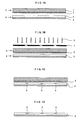
- Fig. 1 shows one example of the method of producing a pattern-formed structure of the present invention.
- a photocatalyst-containing-layer side substrate 3 formed by providing a photocatalyst-containing-layer 2 on a base material 1, and a substrate for a pattern-formed structure 6 formed by providing a characteristic-modifiable layer 5 on a substrate 4, are each prepared (refer to Fig. 1A, process of preparing a substrate for a pattern-formed structure).
- the photocatalyst-containing-layer side substrate 3 and the substrate for a pattern-formed structure 6 are disposed such that the photocatalyst-containing layer 2 faces the characteristic-modifiable layer 5 with a gap or space of a predetermined length therebetween.
- ultraviolet 8 is irradiated from the photocatalyst-containing-layer side substrate 3 side by way of a photomask 7 on which a required pattern has been drawn.
- a pattern constituted of an area 9 whose characteristic has been modified is formed at the surface of the characteristic-modifiable layer 5 (the pattern-forming process).
- a photocatalyst-containing layer formed in a pattern-like configuration or a photocatalyst-containing-layer side substrate including a light-shielding portion formed therein may also be used. In these additional examples, exposure is effected on the whole surface of the substrate for a pattern-formed structure, without using the photomask 7.
- a photocatalyst-containing-layer side substrate used in the below-described pattern forming process is first prepared.
- the photocatalyst-containing-layer side substrate includes a base material and a photocatalyst-containing layer containing a photocatalyst formed on the base material.
- the photocatalyst-containing-layer side substrate includes at least a photocatalyst-containing layer and the base material.
- a film-like photocatalyst-containing layer is formed on a base material by a predetermined method.
- a photocatalyst-containing-layer side substrate including a light-shielding portion formed in a pattern-like configuration can also be used.
- the structure of the photocatalyst-containing layer used in the present invention is not particularly restricted as long as the photocatalyst contained in the photocatalyst-containing layer is capable of modifying the characteristic of the characteristic-modifiable layer.
- the photocatalyst-containing layer may be constituted of a photocatalyst and a binder or constituted of only a photocatalyst of film-like form.
- the wetting property of the photocatalyst-containing layer surface may be either lyophilic or liquid-repellent.
- the photocatalyst-containing layer used in the present invention may be provided on the whole surface of the base material 1, for example, as shown in Fig. 1A.
- the photocatalyst-containing layer 2 may be formed, in a pattern-like configuration, on the base material 1, as shown in Fig. 2.
- the pattern irradiation process using a photomask or the like is no longer required upon energy irradiation in a state in which the photocatalyst-containing layer and the characteristic-modifiable layer are disposed with a gap or space of a predetermined length therebetween, as described below, in the pattern forming process.
- a pattern generated as a result of modification of the characteristic at the characteristic-modifiable layer can be formed by simple energy irradiation on the whole surface of the photocatalyst-containing layer.
- the method of patterning the photocatalyst-containing layer is not particularly restricted, and the photolithography method, for example, may be employed.
- energy irradiation may be effected from any direction, as long as energy is irradiated at the portion where the photocatalyst-containing layer faces the characteristic-modifiable layer.
- the type of irradiated energy is not limited to energy which is applied in a form of parallel light (and the like), which is advantageous.
- Examples of the photocatalyst used in the present invention include titanium dioxide (TiO 2 ), zinc oxide (ZnO), tinoxide (SnO 2 ), strontium titanate (SrTiO 3 ), tungsten oxide (WO 3 ), bismuth oxide (Bi 2 O 3 ) and iron oxide (Fe 2 O 3 ) known as photo-semiconductors.
- TiO 2 titanium dioxide
- ZnO zinc oxide
- SrTiO 3 strontium titanate
- WO 3 tungsten oxide
- Bi 2 O 3 bismuth oxide
- Fe 2 O 3 iron oxide
- One type, or more than one type in combination, of these compounds may be selected for use.
- titanium dioxide is especially preferable for use because titanium dioxide has high band gap energy, is chemically stable, has no toxicity, and is easily available.
- the two types of titanium dioxide i.e., anatase-type titanium dioxide and rutile type titanium dioxide, can be each applicable to the present invention. Anatase-type titanium dioxide is more preferable.
- the excitation wavelength of anatase-type titanium dioxide is 380 nm or less.
- anatase-type titaniumdioxide as described above examples include anatase-type titania sol of hydrochloric acid peptisation type ("STS-02", the average particle diameter is 7 nm, manufactured by Ishihara Sangyo and "ST-K01", manufactured by Ishihara Sangyo), anatase-type titania sol of nitrate acid peptisation type ("TA-15", the average particle diameter is 12 nm, manufactured by Nissan Chemical Industries, Ltd.), and the like.
- STS-02 the average particle diameter is 7 nm, manufactured by Ishihara Sangyo and "ST-K01", manufactured by Ishihara Sangyo
- TA-15 the average particle diameter is 12 nm, manufactured by Nissan Chemical Industries, Ltd.
- the average particle diameter of the photocatalyst to be used is preferably no larger than 50 nm and more preferably no larger than 20 nm.
- the photocatalyst-containing layer of the present invention may be constituted of only the photocatalyst, as described above. However, the photocatalyst-containing layer may be formed as a mixture of the photocatatlys and a binder.
- the photocatalyst is constituted of only the photocatalyst, the efficiency in modification of the characteristic of the characteristic-modifiable layer is improved, which is advantageous in terms of cost reduction because the time required for the treatment can be shortened, for example.
- the photocatalyst-containing layer is constituted of the photocatalyst and the binder, the structure has an advantage that the photocatalyst-containing layer can be formed easily.
- Examples of the method of forming a photocatalyst-containing layer constituted of only the photocatalyst include the spattering method, the CVD method, and a method using a vacuum-film-producing method such as the vacuum deposition method.
- a photocatalyst-containing layer By forming a photocatalyst-containing layer by the vacuum-film-producing method, a photocatalyst-containing layer which is in a form of a uniform film and includes only the photocatalyst can be produced, whereby the characteristic of the characteristic-modifiable layer can be modified evenly.
- the characteristic of the characteristic-modifiable layer can be modified efficiently as compared with the case in which the photocatalyst-containing layer includes a binder.
- Examples of the method of forming a photocatalyst-containing layer constituted of only the photocatalyst include the method of forming amorphous titania on a base material and causing the amorphous titania to phase-change to the crystalline titania by sintering (in the case in which titanium dioxide is used as the photocatalyst).
- the amorphous titania used in the aforementioned method can be obtained, for example, by hydrolysis, dehydrating condensation of inorganic salts of titanium such as titanium tetrachloride, titanium sulfate, or hydrolysis, dehydrating condensation of organic titanium compounds such as tetraethoxytitanium, tetraisopropoxytitatnium, tetra-n-propoxytitanium, tetrabutoxytitanium, tetramethoxytitanium, in the presence of an acid.
- the obtained amorphous titania is denatured to atanase-type titania by sintering at 400 to 500 °C or rutile-type titania by sintering at 600 to 700 °C.
- a binder having a main skeleton whose bonding energy is high enough to prevent itself from being decomposed due to the above-described photo-excitation of the photocatalyst is preferable.
- organopolysiloxane can be raised.
- the above-described photocatalyst-containing layer can be formed by: preparing a coating solution by dispersing the photocatalyst and organopolysiloxane as the binder in a solvent, optionally with other additives; and coating the coating solution on a base material.
- an alcohol-based organic solvent such as ethanol, isopropanol is preferable.
- the coating process may be carried out by any of known coating methods such as spin coating, spray coating, dip coating, roll coating and bead coating.
- the photocatalyst-containing layer can be formed by carrying out the hardening process by irradiating ultraviolet.
- an amorphous silica precursor can also be used as the binder.
- This amorphous silica precursor is preferably a silicon compound represented by the general formula SiX 4 (wherein X is a halogen, the methoxy group, the ethoxy group or the acetyl group) or silanol as a hydrolysate thereof, or polysiloxane whose molecular weight is no larger than 3000.
- a photocatalyst-containing layer can be formed by: evenly dispersing the amorphous silica precursor and the particles of the photocatalyst in non-aqueous solvent; effecting hydrolysis of the components by the moisture in the air, thereby forming silanol on the base material; and effecting dehydrating condensation of silanol at the room temperature.
- the binder of the aforementioned respective types may be used solely or as a combination of two or more types.
- the content of the photocatalyst in the photocatalyst-containing layer may be set in a range of 5 to 60 weight %, and preferably in a range of 20 to 40 weight %.
- the thickness of the photocatalyst-containing layer is preferably in a range of 0.05 to 10 ⁇ m.
- the photocatalyst-containing layer may also contain a surfactant, in addition to the above-mentioned photocatalyst and the binder.
- a surfactant include: a hydrocarbon-based non-ionic surfactant such as NIKKOL BL, BC, BO, BB series manufactured by NIKKO CHEMICALS; a fluorine or silicone-based non-ion surfactant such as ZONYL FSN, FSO manufactured by DuPont Co., Ltd., Surflon S-141, 145 manufactured by Asahi Glass, Megafac-141, 144 manufactured by Dainippon Ink & Chemicals, Futargent F-200, F251 manufactured by Neos Co., Ltd., Unidyne DS-401, 402 manufactured by Daikin Industries, and Frorard FC-170, 176 manufactured by 3M Co., Ltd; a cationic surfactant; an anionic surfactant; and an ampholytic surfactant.
- the photocatalyst-containing layer may further include, in addition to the above-mentioned surfactants, oligomer or polymer of polyvinyl alcohol, unsaturated polyester, acrylic resin, polyethylene, diarylphthalate, ethylenepropylenediene monomer, epoxy resin, phenol resin, polyurethane, melamine resin, polycarbonate, polyvinyl chloride, polyamide, polyimide, styrenebutadiene rubber, chloroprene rubber, polypropylene, polybutylene, polystyrene, polyvinyl acetate, polyester, polybutadiene, polybenzimidazol, polyacrylonitril, epichlorohydrine, polysulfide, and polyisoprene.
- surfactants oligomer or polymer of polyvinyl alcohol, unsaturated polyester, acrylic resin, polyethylene, diarylphthalate, ethylenepropylenediene monomer, epoxy resin, phenol resin, polyurethane, melamine resin, polycarbon
- the photocatalyst-containing-layer side substrate 3 includes at least the base material 1 and the photocatalyst-containing layer 2 formed on the base material 1.
- the material constituting the base material in use is appropriately selected, in consideration of the direction in which energy is irradiated in the pattern forming process described below, whether or not the obtained patter-formed structure needs to be transparent and the like.
- the energy irradiation must (i.e., inevitably) be carried out from the side of the photocatalyst-containing-layer side substrate. That is, energy is irradiated in a state in which the photomask 7 is disposed on the side of the photocatalyst-containing-layer side substrate 3, as shown in Fig. 1B.
- the base material is required to be transparent.
- the pattern-formed structure is transparent, it is possible to irradiate energy in a state in which a photomask is disposed on the side of the substrate for a pattern-formed structure.
- energy must be irradiated from the side of the substrate for a pattern-formed structure.
- the base material does not need to be transparent.
- the base material used in the present invention may be a flexible material such as a film made of a resin or an inflexible material such as a glass substrate.
- the type of the base material is appropriately selected in accordance with the energy irradiation method in the pattern forming process described below.
- the material of the base material used in the photocatalyst-containing-layer side substrate of the present invention is not particularly restricted.
- a material having a predetermined strength and exhibiting excellent adhesion property of the surface thereof to the photocatalyst-containing layer is preferably employed.
- the base material include glass, ceramic, metal, plastics and the like.
- a primer layer may be formed on the base material such that the adhesion between the base material surface and the photocatalyst-containing layer is enhanced.
- the primer layer include a silane-based or titanium-based coupling agent.
- a light-shielding portion formed in a pattern-like configuration may be formed in the photocatalyst-containing-layer side substrate used in the present invention.
- a photocatalyst-containing-layer side substrate having a light-shielding portion is used, either the use of a photomask or the drawing irradiation by laser beam is no longer required at the time of energy irradiation. Accordingly, alignment of the photocatalyst-containing-layer side substrate with the photomask is no longer required, whereby the production process can be made simpler and the expensive device needed for the drawing irradiation by laser beam can be rendered unnecessary, which is advantageous in terms of cost reduction.
- the photocatalyst-containing-layer side substrate having the above-mentioned light-shielding portion can be realized by one of the two embodiments, depending on the position at which the light-shielding portion is formed.
- a photocatalyst-containing-layer side substrate 3 includes a base material 1, a light-shielding portion 13 formed on the base material 1, and a photocatalyst-containing layer 2 formed on the light-shielding portion 13.
- a photocatalyst-containing-layer side substrate 3 includes a base material 1, a photocatalyst-containing layer 2 formed on the base material 1, and a light-shielding portion formed on the photocatalyst-containing layer 2.
- the light-shielding portion is disposed in the vicinity of the photocatalyst-containing layer and the characteristic-modifiable layer facing with a gap therebetween, whereby the influence of the scattering of energy inside the base material can be reduced. As a result, the pattern irradiation of energy can be performed in an extremely accurate manner.
- the light-shielding portion is formed on the photocatalyst-containing layer, by setting the film thickness of the light-shielding portion at the same length as the predetermined distance to be maintained between the photocatalyst-containing layer and the characteristic-modifiable layer, the light-shielding portion can be used as a spacer for keeping the aforementioned distance between the two layers constant when the two layers are disposed so as to face each other.
- the photocatalyst-containing layer and the characteristic-modifiable layer are disposed such that these two layers face each other with a predetermined distance or gap therebetween, by disposing the light-shielding portion and the characteristic-modifiable layer so that these two layers closely contact with each other, the aforementioned gap of the predetermined length can be reliably obtained in an accurate manner.
- a pattern can be precisely formed on the characteristic-modifiable layer by effecting energy irradiation, in this aforementioned state, from the side of the photocatalyst-containing-layer side substrate.
- the method of forming the light-shielding portion as described above is not particularly restricted, and any appropriate method may be selectively employed in accordance with the characteristic of the formation surface of the light-shielding portion or the blocking property thereof with respect to the necessitated energy.
- Examples of the method of forming the light-shielding portion include the spattering method and a method of forming a metal thin film such as chrome having the thickness of 1000 to 2000 ⁇ by the vacuum deposition method or the like and patterning the obtained thin film.
- a conventionally known patterning method such as spattering can be employed.
- Examples of the patterning method also include a method of forming, in a pattern-like configuration, a layer constituted of a resin binder and light-shielding particles, such as carbon fine particles, metal oxides, inorganic pigments, organic pigments, contained in the resin binder.
- the resin binder to be used include: polyimide resin, acrylic resin, epoxy resin, polyacryl amide, polyvinyl alcohol, gelatin, casein, cellulose (the respective types of these resins may be used singly or as a mixture of two or more types); a photosensitive resin; and a resin composition of the O/W emulsion type (such as a resin composition obtained by making a reactive silicone in an emulsion state).
- the thickness of such a light-shielding portion made of resin may be set in a range of 0.5 to 10 ⁇ m.
- the method of patterning the light-shielding portion made of resin include the conventionally known methods such as the photolithography method and the printing method.
- the photocatalyst-containing-layer side substrate includes.a base material, a light-shielding portion formed in a pattern-like configuration on the base material, and the photocatalyst-containing layer formed on the light-shielding portion, it is preferable that a primer layer is provided between the light-shielding portion and the photocatalyst-containing layer.
- the primer layer serves to prevent diffusion of impurities from the light-shielding portion and the opening portion formed in the light-shielding portion (the impurities such as metal, metal ion, residuals generated at the time of patterning the light-shielding portion, in particular) which impurities could be a factor of inhibiting modification of the characteristic of the characteristic-modifiable layer by the photocatalyst. Accordingly, by providing a primer layer, the treatment for effecting modification of the characteristic proceeds in a highly sensitive manner, whereby a pattern can be obtained at a high resolution.
- the primer layer serves to prevent, the impurities present in the light-shielding portion and the opening portion formed in the light-shielding portion, from affecting the effect of the photocatalyst. Therefore, the primer layer is preferably formed at the whole surface of the light-shielding portion, covering the opening portion thereof, as well.
- Fig. 5 shows one example of the photocatalyst-containing-layer side substrate in which a primer layer as described above has been formed.
- the light-shielding portion 13 is formed at one surface of the base material 1, and a primer layer 10 is formed on the same surface of the base material 1 as the light-shielding portion 13 has been formed.
- the photocatalyst-containing layer 2 is formed at the surface of the primer layer 10.
- the structure in which the light-shielding portion is formed, in a patter-like configuration, on the base material is a standard photomask structure. Accordingly, the structure of Fig. 5 is a modification of the standard structure, in which the photocatalyst-containing layer is formed on the photomask by way of a primer layer.
- the primer layer of the present invention is not particularly restricted as long as the primer layer has a structure which prevents the photocatalyst-containing layer from making a physically direct contact with the photomask. In other words, it suffices as long as the light-shielding portion of the photomask is prevented, by the primer layer, from making contact with the photocatalyst-containing layer.
- the material constituting the primer layer is not particularly restricted.
- An inorganic material which is not easily decomposed by the action of the photocatalyst is preferable.
- a specific example thereof is amorphous silica.
- the precursor of the amorphous silica is a silicon compound represented by the general formula SiX 4 (wherein X is a halogen, the methoxy group, the ethoxy group or the acetyl group) and the amorphous silica is silanol as a hydrolysate of the precursors or polysiloxane whose molecular weight is no larger than 3000.
- the thickness of the primer is preferably in a range of 0.001 to 1 ⁇ m, and more preferably in a range of 0.001 to 0.1 ⁇ m.
- the substrate for a pattern-formed structure 6, which is to be disposed at a position opposite to the aforementioned photocatalyst-containing-layer side substrate 3, is prepared, as shown in Fig. 1.
- the type of the substrate for a pattern-formed structure is not particularly restricted as long as the substrate has at least a characteristic-modifiable layer. However, it is preferable that the characteristic-modifiable layer is formed on the substrate, in terms of the strength thereof. Other protective layers or the like may be formed, if necessary, but the characteristic-modifiable layer must be exposed at the whole surface (or at some portions of the surface) on at least one side of the substrate for a pattern-formed structure.
- a substrate for a pattern-formed structure represents a substrate in a state in which a pattern, generated as a result of characteristic modification at certain sites, has not been formed at the characteristic-modifiable layer thereof.
- the substrate for a pattern-formed structure is subjected to exposure and a pattern, generated as a result of characteristic modification at certain sites, has been formed at the characteristic-modifiable layer, the resulting structure is regarded as "a patter-formed structure".
- the characteristic-modifiable layer in the present invention may be prepared as any type of layer, as long as the property or characteristic of the layer is modified by the action of the photocatalyst.
- the characteristic-modifiable layer may be prepared as a layer which is colored by the action of the photocatalyst, by mixing a photochromic mateiral such as spiropyran or an organic colorant which is decomposed by the action of the photocatalyst in the characteristic-modifiable layer.
- the characteristic-modifiable layer may be prepared as a layer in which the attaching property to various substances is enhanced at the exposed portions thereof due to the introduction of a polar group or the roughened state of the surface caused by the photocatalytic effect.
- a pattern exhibiting excellent attaching property can be formed by the pattern exposure.
- a pattern of a metal thin film can be formed by: depositing a metal component on the pattern-formed structure as described above; forming a thin film of metal; and peeling the metal thin film by using an adhesive or a chemical, by utilizing difference in attaching property between the pattern portion and the non-patterned portion of the attaching-property-modifiable layer.
- a pattern of a metal thin film can be formed without forming a pattern at a photoresist, whereby a print wiring board or an electric circuit element and the like, having a more minute and precise pattern than the pattern produced by the printing method, can be formed.
- the above-mentioned characteristic-modifiable layer may be formed by either a dry-type method such as the vacuum deposition method or a wet-type method such as spin coating or dip coating methods.
- the type of the characteristic-modifiable layer is not particularly restricted as long as the layer has various characteristics which are modified by the action of the photocatalyst.
- two particular examples a wetting-property-modifiable layer in which a wetting-property-based pattern is formed as a result of modification of the wetting property of the characteristic-modifiable layer by the action of the photocatalyst; and a decomposable and removable layer in which the characteristic-modifiable layer is decomposed and removed by the action of the photocatalyst, whereby a pattern is formed by the resulting projections and recesses, are especially preferable because these two examples clearly exhibit the advantageous effect of the present invention in the relationship with the resulting functional element or the like.
- the type of the wetting-property-modifiable layer in the present invention is not particularly restricted as long as the wetting property at the surface thereof is modifiable by the action of the aforementioned photocatalyst.
- the characteristic-modifiable layer as the wetting-property-modifiable layer whose wetting property at the surface thereof is modified such that a contact angle formed by a liquid on the surface thereof is decreased by exposure (the term "exposure” represents not only irradiation of light but also irradiation of energy, in the present invention)
- the wetting property of the characteristic-modifiable layer surface can be easily modified in a pattern-like configuration by energy irradiation by way of the light-shielding portion, whereby a pattern constituted of lyophilic areas in which a contact angle formed by a liquid is relatively small can be formed.
- a composition for a functional portion to the lyophilic areas, a functional element can be easily formed. In short, a functional element can be produced efficiently, which is advantageous in terms of cost reduction.
- a lyophilic area represents an area in which a contact angle formed by a liquid is relatively small.
- the lyophilic area is an area which exhibits excellent wetting property for ink for coloring pixel portions (colored layers) as the composition for the functional portion.
- the lyophilic area is an area which exhibits excellent wetting property for the composition forming a microlens.
- a liquid-repellent area represents an area in which a contact angle formed by a liquid is relatively large and thus the wetting property thereof for the above-mentioned composition for the functional portion is relatively poor.
- a contact angle formed on the surface of the unexposed area by a liquid having surface tension of 40 mN/m is to be no smaller than 10°, and it is preferable that a contact angle formed on the same surface by a liquid having surface tension of 30 mN/m is no smaller than 10°, and it is more preferable that a contact angle formed on the same surface by a liquid having surface tension of 20 mN/m is no smaller than 10°.
- the unexposed portion is required to exhibit excellent liquid-repellency. If a contact angle formed by a liquid in the unexposed portion is too small, the liquid-repellency of the portion may not be sufficiently high, whereby there is a possibility that the composition for forming the functional portion remains at the portion, which is not desirable.
- the wetting-property-modifiable layer decreases the magnitude of a contact angle formed by a liquid thereon after being subjected to exposure.
- a contact angle formed on the exposed surface of the wetting-property-modifiable layer by a liquid having surface tension of 40 mN/m is to be no larger than 9°, and it is preferable that a contact angle formed on the same surface by a liquid having surface tension of 50 mN/m is no larger than 10°, and it is more preferable that a contact angle formed on the same surface by a liquid having surface tension of 60 mN/m is no larger than 10°.
- the composition for forming the functional portion may not spread properly at the area, whereby there may arise a problem of undesirably discontinuous distribution of the functional portion and the like.
- a contact angle is obtained as the result of measurement in which a contact angle, formed by a liquid having various surface tension, is measured (30 seconds after dropping drops of the liquid from a microsyringe) by using a contact angle analyzer ("CA-Z type” manufactured by Kyowa Kaimen Kagaku Co., Ltd.) or from the graph plotted based on the results.
- CA-Z type manufactured by Kyowa Kaimen Kagaku Co., Ltd.
- the wetting-index standard solution manufactured by Junsei Kagaku Co., Ltd. was used as the liquids having various surface tension.
- the wetting-property-modifiable layer may be formed as a layer containing fluoride in which the fluoride content of the layer is decreased by energy irradiation thereto, due to the photocatalytic effect, as compared with the fluoride content before the energy irradiation.
- a pattern constituted of the portions at which the fluoride content is low can be formed easily, by pattern-irradiating energy to the wetting-property-modifiable layer.
- fluoride has extremely low surface energy
- the surface of a substance whose fluoride content is relatively high exhibits a relatively low critical surface tension. Therefore, the critical surface tension at a portion whose fluoride content is relatively low is larger than the critical surface tension at the surface of a portion whose fluoride content is relatively high.
- the portion whose fluoride content is relatively low is more lyophilic than the portion whose fluoride content is relatively high. Accordingly, formation of a pattern constituted of portions whose fluoride content is relatively low as compared with the surrounding surface unit formation of a pattern constituted of lyophilic portions in a liquid-repellent area.
- a pattern constituted of lyophilic portions can be easily formed within a liquid-repellent area, by pattern-irradiating energy to the wetting-property-modifiable layer. Therefore, a functional portion can be easily formed only in the lyophilic area, whereby a functional element of excellent quality can be produced at a relatively low cost.
- the fluoride content in the low-fluoride, lyophilic area formed by energy irradiation is, when the fluoride content at the non-energy irradiated portion is expressed as 100, no higher than 10, and preferably no higher than 5, and more preferably no higher than 1.
- the fluoride content in the above-mentioned range, a significantly large difference in the wetting property can be created between the energy-irradiated portion and the non-energy irradiated portion. Accordingly, by forming a functional portion on such a wetting-property-modifiable layer, the functional portion can be formed accurately only in the lyophilic area whose fluoride content has been decreased, whereby a functional element can be obtained in a highly precise manner. It should be noted that rate of decrease in the fluoride content is calculated on the basis of weight.
- Measurement of the fluoride content in the wetting-property-modifiable layer can be carried out by using various conventional methods, such as X-ray Photoelectron Spectroscopy, ESCA (Electron Spectroscopy for Chemical Analysis), fluorescent X-ray Spectroscopy and Mass Spectroscopy.
- the method is not particularly restricted as long as the method allows the quantitative measurement of the fluoride content at a sample surface.
- the type of the material used in the above-mentioned wetting-property-modifiable layer is not particularly restricted, as long as: the characteristic (i.e., the wetting property) of the wetting-property-modifiable layer is modified by exposure, due to the action of the photocatalyst present in the photocatalyst-containing layer which is in contact with the wetting-property-modifiable layer; and the material contains a component having a main chain which is less likely to deteriorate or be decomposed by the action of the photocatalyst. Examples of such a material include:
- the material is preferably organopolysiloxane obtained as a result of hydrolysis condensation or cohydrolysis condensation of at least one type of silicon compound represented by the general formula: Y n SiX (4-n) wherein Y represents a group selected from the group consisting of the alkyl group, the fluoroalkyl group, the vinyl group, the amino group, the phenyl group and the epoxy group, X represents the alkoxyl group, the acetyl group or the halogen group, and n represents an integer of 0 to 3.
- the number of the carbon atom of the group represented by Y is preferably in a range of 1 to 20.
- the alkoxy group represented by X is preferably the methoxy group, the ethoxy group, the propoxy group or the butoxy group.
- Organopolysiloxane containing the fluoroalkyl group can be preferably used.
- Specific examples thereof include hydrolysis condensates or cohydrolysis condensates of one type, or more than two types in combination, of the fluoroalkylsilane described below.
- those conventionally known as the fluorine-based silane coupling agent can be used.
- the liquid-repellency of the unexposed portion of the wetting-property-modifiable layer is significantly enhanced.
- the functional element is a color filter
- the unexposed portion of the wetting-property-modifiable layer excellently prevents the composition for the functional portion, such as ink for coloring pixel portions, from attaching thereto.
- examples of the reactive silicone of the aforementioned (2) include a compound having a skeleton represented by the general formula below.
- n is an integer of 2 or more
- R 1 , R 2 represents a C 1 -C 10 group selected from the group consisting of substituted or unsubstituted alkyl, alkenyl, aryl and cyanoalkyl groups.
- No more than 40 %, in mole ratio, of the whole compound is constituted of vinyl, phenyl or phenyl halide.
- the compound in which R 1 and R 2 are the methyl group is preferable because the surface energy thereof can be reduced to the smallest level. It is preferable that the compound contains no less than 60 %, in mole ratio, of the methyl group.
- the molecular chain includes at least one reactive group such as the hydroxyl group at the chain end or a side chain.
- a stable organosilicone compound such as dimethylpolysiloxane, which does not effect a cross-linking reaction, may further be added to the above-mentioned organopolysiloxane.
- various materials such as organopolysiloxane can be used as the material of the wetting-property-modifiable layer.
- making the wetting-property-modifiable layer contain fluorine is effective for forming a wetting-property-based pattern. Therefore, it is preferable that making, a material which is less likely to deteriorate orbe discomposed by the action of the photocatalyst, contain fluorine, or more specifically, making an organopolysiloxane material contain fluorine to produce a wetting-property-modifiable layer, is preferable.
- Examples of the method of making the organopolysiloxane material contain fluoride include: a method of making a fluorine compound be bound, with relatively low bonding energy, to the main agent having generally a high bonding energy; a method of mixing a fluorine compound, which is bound with relatively low bonding energy, into a wetting-property-modifiable layer.
- the fluorine bonding site at which the bonding energy is relatively low is first decomposed upon irradiation of energy, whereby fluorine can be removed from the wetting-property-modifiable layer.
- Examples of the first method i.e., the method of making a fluorine compound be bound, with relatively low bonding energy, to the main agent having generally a high bonding energy include the method of introducing the fluoroalkyl group as a substituent into the organopolysiloxane.
- organopolysiloxane having high strength can be obtained by hydrolysis and polycondensation of chlorosilane or alkoxysilane by utilizing a sol-gel reaction.
- organopolysiloxane is obtained as a result of hydrolysis condensation or cohydrolysis condensation of at least one type of silicon compound represented by the general formula: Y n SiX (4-n) wherein Y represents a group selected from the group consisting of the alkyl group, the fluoroalkyl group, the vinyl group, the amino group, the phenyl group and the epoxy group, X represents the alkoxyl group, the acetyl group or the halogen group, and n represents an integer of 0 to 3.
- organopolysiloxane including the fluoroalkyl group as the substituent can be obtained.
- the carbon bonding site of the fluoralkyl group is decomposed, upon irradiation of energy, by the action of the photocatalyst present in the photocatalyst-containing layer which is in contact with the wetting-property-modifiable layer, whereby the fluorine content of the energy-irradiated portion of the wetting-property-modifiable layer can be reduced.
- the type of the silicon compound having the fluoroalkyl group used here is not particularly restricted as long as the silicon compound has a fluoroalkyl group.
- a silicon compound which has at least one fluoroalkyl group and the number of the carbon atoms of each fluoroalkyl group is in a range of 4 to 30 (preferably in a range 6 to 20 and more preferably in a range of 6 to 16) is preferably used. Specific examples of such a silicon compound are as described above.
- the silicon compound having a C 6 -C 8 fluoroalkyl group, that is, fluoroalkylsilane is preferable.
- the silicon compound having the above-mentioned fluoroalkyl group may be mixed with the silicon compound not having the above-mentioned fluoroalkyl group and the cohydrolysis condensates thereof may be used as the organopolysiloxane.
- one type or more than one type of the silicon compound having the above-mentioned fluoroalkyl group may be used so that the hydrolysis condensate or cohydrolysis condensate thereof is used as the organopolysiloxane.
- the mole ratio of the silicon compound having the fluoroalkyl group with respect to all the silicon compounds constituting the organopolysiloxane is preferably 0.01 mol % or more, or more preferably 0.1 mol %.
- the content (mole ratio) of the fluroalkyl group contained in the organopolysiloxane is within the above-mentioned range, the liquid-repellency at the wetting-property-modifiable layer can be enhanced, whereby the difference in the wetting property between the liquid-repellent portion and the energy-irradiated, lyophilic area can be increased.
- organopolysiloxane is obtained by cross-linking of a reactive silicone which exhibits excellent liquid-repellency.
- this method as is in the method of the aforementioned (1), by designing at least one of R 1 , R 2 in the aforementioned general formula as a substituent group containing fluorine such as the fluoroalkyl group, it is possible to make the wetting-property-modifiable layer contain fluorine. Further, in this method, the portion of the fluoroalkyl group whose bonding energy is lower than that of the siloxane bonding is decomposed upon irradiation of energy. Accordingly, the fluorine content at the surface of the wetting-property-modifiable layer can be decreased by irradiation of energy.
- examples of the latter method i.e., the method of introducing (mixing) a fluorine compound whose bonding energy is lower than the bonding energy of the binder include: a method of mixing a fluorine-based surfactant (in a case in which a low molecular weight fluorine compound is introduced) ; and mixing a fluorine resin which is highly compatible with the binder resin (in a case in which a high molecular weight fluorine compound is introduced).
- the wetting-property-modifiable layer of the present invention may further include a surfactant.
- a surfactant include: a hydrocarbon-based non-ionic surfactant such as NIKKOL BL, BC, BO, BB series manufactured by NIKKO CHEMICALS; a fluorine or silicone-based non-ion surfactant such as ZONYL FSN, FSO manufactured by DuPont Co., Ltd., Surflon S-141, 145 manufactured by Asahi Glass, Megafac-141, 144 manufactured by Dainippon Ink & Chemicals, Futargent F-200, F251 manufactured by Neos Co., Ltd., Unidyne DS-401, 402 manufactured by Daikin Industries, and Frorard FC-170, 176 manufactured by 3M Co., Ltd; a cationic surfactant; an anionic surfactant; and an ampholytic surfactant.
- a hydrocarbon-based non-ionic surfactant such as
- the wetting-property-modifiable layer may further include, in addition to the above-mentioned surfactants, oligomer or polymer of polyvinyl alcohol, unsaturated polyester, acrylic resin, polyethylene, diarylphthalate, ethylenepropylenediene monomer, epoxy resin, phenol resin, polyurethane, melamine resin, polycarbonate, polyvinyl chloride, polyamide, polyimide, styrenebutadiene rubber, chloroprene rubber, polypropylene, polybutylene, polystyrene, polyvinyl acetate, polyester, polybutadiene, polybenzimidazol, polyacrylonitril, epichlorohydrine, polysulfide, and polyisoprene.
- surfactants oligomer or polymer of polyvinyl alcohol, unsaturated polyester, acrylic resin, polyethylene, diarylphthalate, ethylenepropylenediene monomer, epoxy resin, phenol resin, polyurethane, melamine
- the wetting-property-modifiable layer as described above can be formed by: preparing a coating solution by dispersing the above-mentioned components, and optionally other additives, to a solvent; and applying the coating solution, by coating, to a substrate.
- a solvent an alcohol-based organic solvent such as ethanol, isopropanol is preferable.
- the coating process may be carried out by any of known coating methods such as spin coating, spray coating, dip coating, roll coating and bead coating.
- the wetting-property-modifiable layer can be formed by carrying out the hardening process by irradiating ultraviolet.
- the thickness of the wetting-property-modifiable layer is preferably in a range of 0.001 to 1 ⁇ m, and more preferably in a range of 0.01 to 0.1 ⁇ m, in consideration of the rate of modification of the wetting property effected by the photocatalyst.
- the wetting property of the exposed portion of the wetting-property-modifiable layer can be rendered lyophilic by the action of the photocatalyst present in the photocatalyst-containing layer being in contact with the wetting-property-modifiable layer (or more specifically, by oxidization, decomposition and the like, induced by the photocatalytic effect, of the organic group and the additives as a part of the aforementioned components).
- the type of the wetting-property-modifiable layer used in the present invention is not particularly restricted as long as the wetting property of the layer is modified by the action of the photocatalyst as described above.
- a layer which does not contain photocatalyst is especially preferable.
- the wetting-property-modifiable layer which contains no photocatalyst there is no possibility that the wetting-property-modifiable layer, when the layer is used as a functional element, deteriorates as time elapses and thus the layer can be used for a long period without any trouble.
- wetting-property-modifiable layer is generally formed on a substrate.
- the wetting-property-modifiable layer may be formed of a self-supporting material, so as not to include a substrate.
- the material of the wetting-property-modifiable layer used in the present invention include a material in which a contact angle, formed by a liquid having the same surface tension as that of the composition for the functional portion applied at a later stage, changes by at least 1°, preferably at least 5°, and more preferably at least 10°, by irradiating energy in a state in which the photocatalyst-containing layer is in contact with the wetting-property-modifiable layer.
- wetting-property-modifiable layer is made of a material which transmits the irradiated energy.
- Such a material examples include polyethylene, polycarbonate, polypropylene, polystyrene, polyester, polyvinylfluoride, acetal resin, nylon, ABS, PTFE, methacryl resin, phenol resin, polyvinylidene fluoride, polyoxymethylene, polyvinyl alcohol, polyvinyl chloride, polyethylene terephthalate, silicone and the like.
- the decomposable and removable layer is a layer whose exposed portion is decomposed and removed, at time of exposure, by the action of the photocatalyst in the photocatalyst-containing layer.
- the exposed portion of the decomposable and removable layer is decomposed and removed by the action of the photocatalyst. Therefore, a pattern constituted of a portion having the decomposable and removable layer and a portion not having the decomposable and removable layer i.e., a pattern having recesses and projections can be formed without carrying out the development or washing process. Accordingly, a member which necessitates a recess-projection pattern, such as a printing plate of various types, can be easily formed by this method.
- this decomposable and removable layer by applying this decomposable and removable layer to a screen by coating and effecting pattern-exposure in a state in which the screen is in contact with the photocatalyst-containing-layer side substrate, thereby decomposing and removing the decomposable and removable layer of the exposed portion, an original plate for screen printing can be formed without carrying out the development and/or washing process.
- the decomposable and removable layer is made of a material having photoresist characteristic, a pattern of the photoresist can be easily formed by effecting pattern exposure in a state in which the decomposable and removable layer is in contact with the photocatalyst-containing-layer side substrate. Accordingly, such a decomposable and removable layer can be employed as a photoresist which does not necessitate either development or washing process, in the semiconductor producing process and the like.
- the decomposable and removable layer is oxidized and decomposed by the action of the photocatalyst at the time of exposure and eventually vaporized. That is, the decomposable and removable layer is removed without carrying out any specific post-treatment such as developing and/or washing process. However, the washing process and the like may be carried out, depending on the material of the decomposable and removable layer.
- a pattern can be formed by not only creating recess and projections at the layer surface but also utilizing the difference in the surface characteristic between the decomposable and removable layer and the base material exposed as a result of decomposition and removal of the layer.
- a surface characteristic include various characteristics like the attaching property and the color-developing property.
- the wetting property is raised, in particular, as the useful surface characteristic. Forming a pattern on the basis of the difference in the wetting property is preferable in terms of the effectiveness when an element is finally formed.
- the decomposable and removable layer is designed such that a contact angle formed by a liquid on the decomposable and removable layer is different from a contact angle formed by the same liquid on the substrate exposed as a result of decomposition-removal of the decomposable and removable layer. It is especially preferable that a contact angle formed by a liquid on the decomposable and removable layer is larger than a contact angle formed by the same liquid on the substrate.
- the liquid-repellency as expressed as a contact angle formed by a liquid having the same surface tension as that of the composition for the functional portion applied by coating at a later stage, is to be at least 30°, preferably at least 40°, and more preferably at least 50°.
- the material which can be preferably used for the decomposable and removable layer include a functional thin film i.e., a Self-Assembled Monolayer Film, a Langmuir-Blodgett's Film and a Layer-by-Layer Self-Assembled Film.
- a fluorine-base resin can also be used for the decomposable and removable layer.
- a Self-Assembled Monolayer Film is a monolayer generated as a result of adsorption and bonding of suitable molecules on a suitable substrate surface (self-assembling of molecules).
- Examples of a material capable of forming a self-assembled layer include surfactant molecules such as fatty acids, organic silicon molecules such as alkyltrichlorosilanes and alkylalkoxides, organic sulfur molecules such as alkanethiols, and organic phosphoric molecules such as alkylphosphates.
- surfactant molecules such as fatty acids
- organic silicon molecules such as alkyltrichlorosilanes and alkylalkoxides
- organic sulfur molecules such as alkanethiols
- organic phosphoric molecules such as alkylphosphates.
- the common characteristics, in general, in the molecule structures of the above-mentioned compounds is that each type of molecule has a relatively long alkyl chain and a functional group located at one molecular end, which functional group interacts the substrate surface.
- the alkyl chain portion is the source of the intermolecular force at the time of packing of molecules in the two-dimensional manner.
- a Self-Assembled Monolayer Film include those composed of various molecules, such as: a Self-Assembled Monolayer Film having a functional group like the amino group or the carboxyl group at the other end of the molecule; a Self-Assembled Monolayer Film whose alkylene chain portion is the oxyethylene chain; a Self-Assembled Monolayer Film whose alkylene chain portion is the fluorocabon chain; a Self-Assembled Monolayer Film whose alkylene chain portion is a composite chain of the oxyethylene chain and the fluorocarbon chain.
- a composite-type Self-Assembled Monolayer Film constituted of plural types of molecular species is also acceptable.
- the present invention includes these two structures (the polymer brush etc.,) into the category of Self-Assembled Monolayer Film.
- the Langmuir-Blodgett's Film used in the present invention after being formed on a substrate, is not so significantly different in shape thereof from the above-mentioned Self-Assembled Monolayer Film.
- the unique feature of the Langmuir-Blodgett's Film resides in the method of forming the film and the excellent, two-dimensional molecular packing property (excellent orientation, excellent order) resulted from the method.
- the molecules for forming the Langmuir-Blodgett's Film are in general developed on a gas-liquid interface first and the developed film is condensed by trough, whereby the developed film is modified to a condensed film which has been highly packed.
- the condensed film is transferred to an appropriate substrate for use.
- a Langmuir-Blodgett's Film of various types can be formed by the method schematically described herein. Further, not only low-molecular weight materials, but also macro molecular materials and colloidal particles may also be used as the film material. Regarding the recent cases in which various materials have been applied, detailed description can be found in the text "Prospect of Nanotechnology created by Soft-based Nanodevice", Macro Molecule, vol. 50, September, 644-647 (2001).
- the Layer-by-Layer Self-Assembled Film is generally a film formed by successively, in the laminating manner, providing a material having at least two positively or negatively charged functional groups on a substrate by adsorption and bonding.
- a material having many functional groups is advantageous in terms of the strength and durability of the film, ionic polymers (high polymer electrolytes) are often used as the material, recently.
- Particles having surface charge such as protein, metal or oxide, what is called “colloidal particles” are also often used as a film-forming substance. More recently, films which make the best use of the interactions weaker than the ionic bond, such as hydrogen bond, coordinate bond, hydrophobic interaction, have been reported.
- the Layer-by-Layer Self-Assembled Film is, when the simplest process for formation thereof is taken as an example, a layer formed by repeating, predetermined times, the cycle of: adsorption of the material having positive (negative) charge; washing; adsorption of the material having negative (positive) charge; and washing.
- the Layer-by-Layer Self-Assembled Film there is no necessity of carrying out an operation of development, condensation and transfer, as is required in the Langmuir-Blodgett's Film.
- the Layer-by-Layer Self-Assembled Film generally does not exhibit the two-dimensional, excellent orientation and order as the Langmuir-Blodgett's Film has.
- the Layer-by-Layer Self-Assembled Film and the production process thereof have a lot of advantages which the conventional film-forming methods lack, which advantages include that a flawless and dense layer can be easily formed and that a layer can be formed evenly even on a surface having minute recesses andprojections, the inner surface of a tube, a sphere surface and the like.
- the thickness of the decomposable and removable layer is not particularly restricted as long as the layer thickness is thin enough to be decomposed and removed by the energy irradiated in the energy irradiating process described below.
- the specific layer thickness is preferably in a range of 0.001 to 1 ⁇ m, and more preferably in a range of 0.01 to 0.1 ⁇ m, although the thickness may significantly vary depending on the type of the irradiated energy and the material of the decomposable and removable layer.
- the characteristic-modifiable layer is preferably formed on a substrate 4, as shown in Fig. 1, in order to gain sufficient strength thereof and ensure good performance of the eventually obtained functional element.
- the substrate include, depending on the state of application of the pattern-formed structure or the functional element produced by using the pattern-formed structure, glass, metal such as aluminum and an alloy thereof, plastic, woven cloth, and unwoven cloth.
- the photocatalyst-containing layer and the characteristic-modifiable layer are then disposed so as to have a gap therebetween of no larger than 200 ⁇ m, but not to be in contact with each other. Thereafter, a pattern forming process is carried out in which energy is irradiated from a predetermined direction.
- the photocatalyst-containing layer and the characteristic-modifiable layer so as to have a gap or space of a predetermined distance therebetween, oxygen, water and active oxygen species generated by the action of the photocatalyst can be easily removed/attached. Specifically, if the gap between the photocatalyst-containing layer and the characteristic-modifiable layer is narrower than the above-mentioned range, there is a possibility that removal/attachment of the aforementioned active oxygen species is disturbed and thus the rate of modification of the characteristic is slowed, which is not desirable.
- the gap between the photocatalyst-containing layer and the characteristic-modifiable layer is wider than the above-mentioned range, the generated active oxygen species is significantly prevented from reaching the characteristic-modifiable layer and thus the rate of modification of the characteristic may be slowed, which is not desirable, either.
- the above-mentioned gap is preferably in a range of 0.2 to 10 ⁇ m, and more preferably in a range of 1 to 5 ⁇ m, in order to achieve very good pattern precision and sufficiently high sensitivity of the photocatalyst, which results in highly efficient modification of the characteristic.
- the gap or distance of the above-mentioned range is especially effective in a substrate for a pattern-formed structure having a small area, in which the above-mentioned gap can be controlled with high precision.
- the above-mentioned gap between the two layers is set preferably in a range of 10 to 100 ⁇ m, and more preferably in a range of 50 to 75 ⁇ m.
- the setting of the gap, at the aligning device in the exposure device, between a photocatalyst-containing-layer side substrate and a substrate for a pattern-formed structure is preferably in a range of 10 to 200 ⁇ m, and more preferably in a range of 25 to 75 ⁇ m.
- a method of using a spacer can be raised.
- an even gap or space can be maintained between the two layers.
- the action of the photocatalyst does not reach the surface of the portion of the characteristic-modifiable layer at which portion the spacer is in contact with the characteristic-modifiable layer. Therefore, by designing the spacer so as to have the same pattern as the above-mentioned pattern, a predetermined pattern can be formed on the characteristic-modifiable layer.
- the spacer may be formed as one independent or separate member.
- the spacer is formed on the surface of the photocatalyst-containing layer of the photocatalyst-containing-layer side substrate, so as to function as both spacer and light-shielding portion.
- the spacer has the function of the light-shielding portion.
- the spacer may be formed of the material not to have the functionof shielding the irradiated energy, because the spacer is enough to have the function not to affect the portion of the characteristic-modifiable layer underneath the spacer.
- energy irradiation represents any conception of energy irradiation which can cause the photocatalyst-containing layer to modify the characteristic of the characteristic-modifiable layer and is not restricted to irradiation of visual light.
- the wavelength of light used in such exposure is generally set in a range of 400 nm or less, and preferably in a range of 380 nm or less, because the preferable photocatalyst used in the photocatalyst-containing layer is titanium dioxide as described above and light having wavelength within the aforementioned range is preferable as energy for activating the photocatalytic effect by titanium dioxide.
- Examples of the light source which can be used for such exposure include mercury lamp, metal halide lamp, xenon lamp, eximer lamp and other light source of various types.
- the method of carrying out drawing irradiation according to a pattern by using a laser such as eximer, YAG or the like is also acceptable.
- the amount of energy irradiation during exposure is set at the amount of irradiation which is necessary for causing the photocatalyst in the photocatalyst-containing layer to act on the surface of the characteristic-modifiable layer, thereby to modify the characteristic at the surface of the characteristic-modifiable layer.
- the photocatalyst-containing layer is heated during exposure because the sensitivity can be increased and thus modification of the characteristic canbeeffectedefficiently. Specifically, itispreferable that heating of the photocatalyst-containing layer is carried out in a range of 30° to 80°.
- the direction in which exposure is performed is determined in consideration of the pattern forming method (whether or not the light-shielding portion is formed on the photocatalyst-containing-layer side substrate) and whether the photocatalyst-containing-layer side substrate or the substrate for a pattern-formed structure is transparent or not.
- the light-shielding portion in a case in which the light-shielding portion is formed in the photocatalyst-containing-layer side substrate, exposure needs to be done from the side of the photocatalyst-containing-layer side substrate and the photocatalyst-containing-layer side substrate needs to be transparent with respect to energy.
- the direction in which exposure is effected may be from either the side of the photocatalyst-containing-layer side substrate or the side of the substrate for a pattern-formed structure.
- exposure may be effected from any direction, as described above, as long as energy is irradiated to the facing portions of the photocatalyst-containing layer and the characteristic-modifiable layer.
- energy may be irradiated from any direction, as long as energy is irradiated to the facing portions of the photocatalyst-containing layer and the characteristic-modifiable layer.
- the substrate on which the photomask has been arranged i.e., the photocatalyst-containing-layer side substrate or the substrate for a pattern-formed structure
- the substrate on which the photomask has been arranged i.e., the photocatalyst-containing-layer side substrate or the substrate for a pattern-formed structure
- the photocatalyst-containing-layer side substrate is removed from the position at which the photocatalyst-containing-layer side substrate was facing the characteristic-modifiable layer, whereby a pattern constituted of the characteristic-modified area 9 in which the characteristic has been modified is formed on the characteristic-modifiable layer 5 as shown in Fig. 1D.
- the type of the modification of the characteristic of the characteristic-modifiable layer surface in the pattern forming process can be classified into two main categories.
- One type of the modification is to modify the characteristic at the surface of the characteristic-modifiable layer, and the other type of the modification is to remove some portions thereof.
- the compound at the characteristic-modifiable layer surface is modified by the action of the photocatalys, whereby the chemical and/or physical characteristics of the compound are changed.
- the resistivity value at the surface is to be changed, such a change can be achieved bymodifying the chemical activity of the surface, modifying the adhesion property at the surface or by other methods.
- the above-mentioned wetting-property-modifiable layer is one typical example thereof.
- the cases in which the characteristic-modifiable layer is removed by the action of the photocatalyst induced by energy irradiation are also included into modification of the characteristic of the characteristic-modifiable layer of the present invention.
- these cases include: the case in which the characteristic-modifiable layer on the substrate is removed only at the energy-irradiated portions thereof; the case in which recesses are formed at the characteristic-modifiable layer surface only at the energy-irradiated portions thereof; the case in which removal of the characteristic-modifiable layer surface occurs locally as a result of energy irradiation, whereby recesses and projections are created at the surface; and the like.
- the typical example of these cases is the above-mentioned decomposable and removable layer.
- a pattern-formed structure can be obtained by forming a pattern, produced as a result of modification of the characteristic, on the above-mentioned substrate for a pattern-formed structure. Then, functional elements of various types can be produced by attaching a composition for forming a functional portion to the obtained pattern of the pattern-formed structure.
- Such functional elements have the characteristic in that the functional portion thereof is formed according to the above-mentioned pattern of the pattern-formed structure.
- a functional portion represents that the portion can effect various functions including: optical functions (such as light-selective absorption, reflection, polarization, light-selective transmittance, non-linear optical character, luminescence like fluorescence or phosphorescence, and photochromism); magnetic functions (such as hard magnetic, soft magnetic, non-magnetic functions, magnetism-transmittance); electric/electronic functions (such as electrical conductivity, insulation, piezoelectricity, pyroelectricity, dielectric function); chemical functions (such as adsorption, desorpion, catalytic function, hydrophilicity, ion-conductivity, oxidizing/reducing function, electrochemical characteristic, electrochromic); mechanical functions (such as wear resistance); thermal functions (heat transmitting property, adiathermancy, infrared radiation); and biodynamical functions (such as biocompatibility, anti-thrombogenic function).
- optical functions such as light-selective absorption, reflection, polarization, light-selective transmitt
- the arrangement of the functional portion as described above to the site corresponding to the pattern of the pattern-formed structure is carried out by a method utilizing difference in the wetting property or the adhesion property between the lyophilic and liquid-repellent areas.
- the composition for the functional portion when the composition for the functional portion is coated on the pattern-formed structure, the composition for the functional portion is attached only to the lyophilic area which exhibits excellent wetting property, whereby the functional portion can be arranged easily only at the pattern of the lyophilic area of the pattern-formed structure.
- the type of the composition for the functional portion used in the present invention significantly varies depending on the function and the forming method of the functional element.
- the composition of the functional portion is a metal.
- a composition which has not been diluted by a solvent typically represented by UV-hardening monomer
- a composition which has been diluted by a solvent i.e., in a form of liquid
- the solvent is preferably that which exhibits high surface tension such as water or ethyleneglycol.
- a composition having the lower viscosity is the more preferable because the more quickly a pattern can be formed.
- the solvent is low volatile.
- composition for the functional portion used in the present invention may directly constitute the functional portion by being attached and arranged on the pattern-formed structure.
- the composition for the functional portion may constitute the functional portion by being arranged on the pattern-formed structure and then treatedwith a chemical, ultraviolet, heat or the like.
- the composition for the functional portion containing a component which is hardened by ultraviolet, heat, electron beam or the like as a binder is preferable because the functional portion can be formed quickly by carrying out the hardening process.
- a functional portion can be formed on the pattern of the lyophilic-area at the surface of the pattern-formed structure, by coating the composition for the functional portion on the pattern-formed structure surface by using a coating unit such as dip coating, roll coating, blade coating and spin coating or a nozzle-discharge unit such as ink-jet.
- a coating unit such as dip coating, roll coating, blade coating and spin coating
- a nozzle-discharge unit such as ink-jet.
- a functional element having a pattern of a metal film as the functional portion thereof can be obtained.
- a functional element having a desired metal pattern on the wetting-property-modifiable layer can be obtained by: treating only the lyophilic area at the wetting-property-modifiable layer surface of the pattern-formed structure with preparation liquid for chemical plating, by utilizing the difference in the wetting property; and immersing the treated pattern-formed structure in a chemical plating solution.
- a pattern of metal can be formed without necessity of forming a resist pattern. Therefore, by this method, a printed wiring board or an electric circuit element can be produced as a functional element.
- a functional portion may be formed according to a pattern, by arranging the composition for the functional portion on the whole surface of the characteristic-modifiable layer and then removing the composition at unnecessary portions by utilizing difference in the wetting property between the liquid-repellent and lyophilic areas.
- a pattern of a functional portion can be obtained by utilizing difference in the adhesion property between the lyophilic and liquid repellent areas of the wetting-property-modifiable layer, for example, by removing the composition at the unnecessary portions by peeling closely attaching a sticky tape to the wetting-property-modifiable layer and then peeling the tape off, air blowing, or post-treatment such as a treatment by a solvent.
- composition for the functional portion on the whole surface of the wetting-property-modifiable layer of the pattern-formed structure of the present invention.
- methods of effecting such an arrangement include the vacuum film-forming method such as PVD, CVD.
- the functional element obtained in a such manner include a color filter, a microlens, a print wiring board, an electric circuit element and the like.
- a color filter is used in a liquid crystal display and the like.
- a color filter a plurality of pixel portions such as red, green and blue are formed on a glass substrate or the like in a highly precise pattern.
- the pixel portions (the functional portions) can be easily formed by attaching ink (the composition for the functional portion) to the above-mentioned lyophilic area of the pattern-formed structure, by way of an ink-jet device or the like, and hardening the ink.
- ink the composition for the functional portion
- a color filter can be produced in a highly elaborate and precise manner by a production process including fewer number of processes.
- the light-shielding portion of the aforementioned pattern-formed structure can be used as it is as a black matrix in the color filter. Accordingly, by forming pixel portions (colored portions) as a functional portion on the aforementioned pattern-formed structure of the present invention, a color filter can be obtained without necessity of forming a black matrix separately.
- the photomask of the present invention can be realized by at least three embodiments.
- a photomask of the first embodiment includes a transparent base material, a light-shielding portion pattern having thickness of 0.2 to 10 ⁇ m and formed, in a pattern-like configuration, on the transparent base material, and a photocatalyst-containing layer formed on the transparent base material and the light-shielding portion pattern.
- a specific example thereof is shown in Fig. 3.
- the photocatalyst-containing-layer side substrate which includes the light-shielding portion can be used as a photomask, due to the functional feature thereof.
- a photomask of the second embodiment includes a transparent base material, a photocatalyst-containing layer formed on the transparent base material, and a light-shielding portion pattern having thickness of 0.2 to 10 ⁇ m and formed, in a pattern-like configuration, on a photocatalyst-containing layer.
- a specific example thereof is shown in Fig. 4.
- a photomask of the third embodiment includes a transparent base material, a light-shielding portion formed, in a pattern-like configuration, on the transparent base material, a primer layer formed on the transparent base material and the light-shielding portion, and the photocatalyst-containing layer formed on the primer layer.
- a specific example thereof is shown in Fig. 5.
- a titanium oxide coating agent for photocatalyst (TKC301, manufactured by TEIKA Co., Ltd.) was applied by coating.
- the substrate was dried at 350 °C for 3 hours, whereby a photomask including a photocatalyst-containing layer (the photocatalyst-containing-layer side substrate) was obtained.
- the photomask and the substrate for a pattern-formed structure obtained as described above were closely attached to each other and ultraviolet was irradiated by an extra-high pressure mercury lamp at the illumination intensity of 20 mW/cm 2 (365 nm) from the photomask side, whereby a wetting-property based pattern was formed at the surface of the wetting-property-modifiable layer.
- the contact angle formed by water at the unexposed portion of the wetting-property-modifiable layer was 72° and it took 120 seconds for the contact angle formed by water at the exposed portion of the wetting-property-modifiable layer to decrease to 10° or smaller.
- the width of the unexposed portion at the wetting-property-modifiable layer surface was 95 ⁇ m and the width of the exposed portion at the wetting-property-modifiable layer surface was 105 ⁇ m.
- a pattern formation was carried out in the substantially same manner as that of example 1, except that the thickness of the chrome-made pattern-formed structure was 0.1 ⁇ m. As a result, it took 370 seconds for the contact angle formed by water at the exposed portion of the wetting-property-modifiable layer to decrease to 10° or smaller.
- a pattern formation was carried out in the substantially same manner as that of example 1, except that the light-shielding portion pattern of example 1 was replaced with a light-shielding portion pattern having thickness of 20 ⁇ m and made of a resin binder in which carbon black had been dispersed. As a result, it took 560 seconds for the contact angle formed by water at the exposed portion of the wetting-property-modifiable layer to decrease to 10° or smaller.
- a pattern formation was carried out in the substantially same manner as that of example 1, except that the photomask and the wetting-property-modifiable layer were not closely attached to each other, but a gap (10 ⁇ m) was set between the wetting-property-modifiable layer and the photocatalyst-containing layer formed on the light-shielding portion pattern. As a result, it took 120 seconds for the contact angle formed by water at the exposed portion of the wetting-property-modifiable layer to decrease to 10° or smaller.
- the width of the unexposed portion at the wetting-property-modifiable layer surface was 80 ⁇ m and the width of the exposed portion at the wetting-property-modifiable layer surface was 120 ⁇ m.
- a coating solution for primer layer which had been prepared by mixing the components of the composition described below and stirring the mixture at 25 °C for 24 hours, was applied by coating.
- the photomask was heated at 120 °C for 20 minutes, whereby a primer layer having thickness of 0.1 ⁇ m was formed.
- an inorganic coating agent for photocatalyst (ST-K01, manufactured by Ishihara Sangyo) was applied by coating on the primer layer.
- the photomask was then heated at 150 °C for 20 minutes such that a photocatalyst-containing layer having thickness of 0.15 ⁇ m was formed, whereby a photomask containing the photocatalyst (the photocatalyst-containing-layer side substrate) was formed.
- a coating solution for fluorine-based silicone which had been prepared by mixing the components of the composition described below and stirring the mixture at 25 °C for 24 hours, was applied by coating on a glass substrate.
- the glass substrate was then dried at 120 °C for 15 minutes, whereby a characteristic-modifiable layer having thickness of 0.05 ⁇ m was formed.
- the photomask and the substrate for a pattern-formed structure obtained as described above were closely attached to each other and ultraviolet was irradiated by an extra-high pressure mercury lamp at the illumination intensity of 20 mW/cm 2 (365 nm) from the photomask side, whereby a wetting-property based pattern was formed at the surface of the characteristic-modifiable layer.
- the contact angle formed by water at the unexposed portion of the characteristic-modifiable layer was 106° and it took 120 seconds for the contact angle formed by water at the exposed portion of the characteristic-modifiable layer to decrease to 10° or smaller.
- the width of the unexposed portion at the characteristic-modifiable layer surface was 49 ⁇ m and the width of the exposed portion at the characteristic-modifiable layer surface was 51 ⁇ m.
- a pattern formation was carried out in the substantially same manner as that of example 5, except that a photomask containing the photocatalyst was formed without including a primer layer. As a result, it took 240 seconds for the contact angle formed by water at the exposed portion of the characteristic-modifiable layer to decrease to 10° or smaller.
- the width of the unexposed portion at the characteristic-modifiable layer surface was 40 ⁇ m and the width of the exposed portion at the characteristic-modifiable layer surface was 60 ⁇ m.
- a coating solution for primer layer which had been prepared by mixing the components of the composition described below and stirring the mixture at 25 °C for 24 hours, was applied by coating.
- the photomask was heated at 120 °C for 20 minutes, whereby a primer layer having thickness of 0.1 ⁇ m was formed.
- an inorganic coating agent for photocatalyst (ST-K03, manufactured by Ishihara Sangyo) was applied by coating on the primer layer.
- the photomask was then heated at 150 °C for 20 minutes such that a photocatalyst-containing layer having thickness of 0.15 ⁇ m was formed, whereby a photomask containing the photocatalyst (the photocatalyst-containing-layer side substrate) was formed.
- a coating solution for fluorine-based silicone which had been prepared by mixing the components of the composition described below and stirring the mixture at 25 °C for 24 hours, was applied by coating on a glass substrate of 370 ⁇ 470 mm. The glass substrate was then heated at 120 °C for 15 minutes, whereby a characteristic-modifiable layer having thickness of 0.05 ⁇ m was formed.
- the photomask and the substrate for a pattern-formed structure prepared as described above were closely attached to each other so as to have a gap of 60 ⁇ m therebetween by using a large-size automatic exposure device (MA-6000 series, manufactured by Dainippon KaKen Co., Ltd.).
- Ultraviolet was irradiated at the illumination intensity of 20 mW/cm 2 (365 nm) from the photomask side, whereby a wetting-property based pattern was formed at the surface of the characteristic-modifiable layer.
- the gaps actually measured at four sites between the photomask and the substrate for a pattern-formed structure were all within a range of 53 to 64 ⁇ m.
- the contact angle formed by a wetting property standard reagent (40 mN/m) at the unexposed portion of the wetting-property-modifiable layer was 75° and it took 150 seconds for the contact angle formed by the wetting property standard reagent (40 mN/m) at the exposed portion of the characteristic-modifiable layer to decrease to 9° or smaller.
- the width of the unexposed portion at the wetting-property-modifiable layer surface was 49 ⁇ m and the width of the exposed portion at the wetting-property-modifiable layer surface was 51 ⁇ m.
- a pattern formation was carried out in the substantially same manner as that of example 6, except that the gap between the photomask and the substrate for a pattern-formed structure was set at 150 ⁇ m.
- the gaps actually measured at four sites between the photomask and the substrate for a pattern-formed structure were all within a range of 145 to 152 ⁇ m.
- the width of the unexposed portion at the wetting-property-modifiable layer surface was 47 ⁇ m and the width of the exposed portion at the wetting-property-modifiable layer surface was 53 ⁇ m.
- a pattern formation was carried out in the substantially same manner as that of example 6, except that the gap between the photomask and the substrate for a pattern-formed structure was set at 250 ⁇ m. As a result, it took 360 seconds for the contact angle formedby the wetting property standard reagent (40 mN/m) at the exposed portion of the characteristic-modifiable layer to decrease to 9° or smaller.
- the width of the unexposed portion at the wetting-property-modifiable layer surface was 15 ⁇ m and the width of the exposed portion at the wetting-property-modifiable layer surface was 85 ⁇ m.
- a pattern formation was carried out in the substantially same manner as that of example 6, except that the gap between the photomask and the substrate for a pattern-formed structure was set at 5 ⁇ m.
- the photocatalyst-containing layer and the characteristic-modifiable layer were in contact with each other at some portions. As a result, there was generated unevenness in the degree of modification of the wetting property in the characteristic-modifiable layer, whereby a unique pattern was not be obtained.
- a coating solution for primer layer which had been prepared by mixing the components of the composition described below and stirring the mixture at 25 °C for 24 hours, was applied by coating.
- the photomask was heated at 120 °C for 20 minutes, whereby a primer layer having thickness of 0.1 ⁇ m was formed.
- an inorganic coating agent for photocatalyst (ST-K03, manufactured by Ishihara Sangyo) was applied by coating on the primer layer.
- the photomask was then heated at 150 °C for 20 minutes such that a photocatalyst-containing layer having thickness of 0.15 ⁇ m was formed, whereby a photomask containing the photocatalyst (the photocatalyst-containing-layer side substrate) was formed.
- a substrate formed by vapor-depositing gold on a glass substrate was immersed for 24 hours in a Self-Assembled Film composition which had been prepared by dissolving octadecanethiol in hexane, whereby a decomposable and removable layer was formed on the glass substrate by way of gold.
- the photomask and the substrate for a pattern-formed structure prepared as described above were closely attached to each other and ultraviolet was irradiated by an extra-high pressure mercury lamp at the illumination intensity of 20 mW/cm 2 (365 nm) from the photomask side, whereby a wetting-property based pattern was formed at the surface of the characteristic-modifiable layer.
- the width of the unexposed portion at the characteristic-modifiable layer surface was 49 ⁇ m and the width of the exposed portion at the characteristic-modifiable layer surface was 51 ⁇ m.
Landscapes
- General Physics & Mathematics (AREA)
- Physics & Mathematics (AREA)
- Engineering & Computer Science (AREA)
- Chemical & Material Sciences (AREA)
- Nanotechnology (AREA)
- Structural Engineering (AREA)
- Architecture (AREA)
- Composite Materials (AREA)
- Crystallography & Structural Chemistry (AREA)
- Materials Engineering (AREA)
- Condensed Matter Physics & Semiconductors (AREA)
- Optical Filters (AREA)
- Materials For Photolithography (AREA)
- Catalysts (AREA)
- Photosensitive Polymer And Photoresist Processing (AREA)
- Exposure Of Semiconductors, Excluding Electron Or Ion Beam Exposure (AREA)
Abstract
Description

| 0.1 N hydrochloric acid (aq) | 50 g |
| Tetramethoxysilane | 100 g |
| 0.2 N hydrochloric acid (aq) | 25 g |
| Fluoroalkylsilane | 15 g |
| Tetramethoxysilane | 50 g |
| 0.1 N hydrochloric acid (aq) | 50 g |
| Tetramethoxysilane | 100 g |
| 0.2 N hydrochloric acid (aq) | 25 g |
| Fluoroalkylsilane | 15 g |
| Tetramethoxysilane | 50 g |
| 0.1 N hydrochloric acid (aq) | 50 g |
| Tetramethoxysilane | 100 g |
Claims (3)
- A photomask, comprising:a transparent base material;a light-shielding portion defining a pattern on the transparent base material;a primer layer formed on the transparent base material and the light-shielding portion; anda photocatalyst-containing layer formed on the primer layer.
- A photomask, comprising:a transparent base material;a photocatalyst-containing layer formed on the transparent base material; anda light-shielding portion defining a pattern on the photocatalyst-containing layer, such that the shielding portion has thickness from 0.2 to 10 µm.
- A photomask, comprising:a transparent base material;a light-shielding portion defining a pattern configuration on the transparent base material, such that the shielding portion has thickness from 0.2 to 10 µm; anda photocatalyst-containing layer formed on the transparent base material and the light-shielding portion.
Applications Claiming Priority (7)
| Application Number | Priority Date | Filing Date | Title |
|---|---|---|---|
| JP2001096012 | 2001-03-29 | ||
| JP2001096012 | 2001-03-29 | ||
| JP2001355410 | 2001-11-20 | ||
| JP2001355410 | 2001-11-20 | ||
| JP2002020947 | 2002-01-30 | ||
| JP2002020947 | 2002-01-30 | ||
| EP02252352A EP1246011B1 (en) | 2001-03-29 | 2002-03-28 | Method of producing a pattern |
Related Parent Applications (1)
| Application Number | Title | Priority Date | Filing Date |
|---|---|---|---|
| EP02252352A Division EP1246011B1 (en) | 2001-03-29 | 2002-03-28 | Method of producing a pattern |
Publications (2)
| Publication Number | Publication Date |
|---|---|
| EP1517177A2 true EP1517177A2 (en) | 2005-03-23 |
| EP1517177A3 EP1517177A3 (en) | 2008-02-20 |
Family
ID=27346397
Family Applications (3)
| Application Number | Title | Priority Date | Filing Date |
|---|---|---|---|
| EP02252352A Expired - Lifetime EP1246011B1 (en) | 2001-03-29 | 2002-03-28 | Method of producing a pattern |
| EP04030777A Expired - Lifetime EP1517180B1 (en) | 2001-03-29 | 2002-03-28 | Method of producing a pattern |
| EP04030778A Withdrawn EP1517177A3 (en) | 2001-03-29 | 2002-03-28 | Method of producing a pattern and photomask used in the same |
Family Applications Before (2)
| Application Number | Title | Priority Date | Filing Date |
|---|---|---|---|
| EP02252352A Expired - Lifetime EP1246011B1 (en) | 2001-03-29 | 2002-03-28 | Method of producing a pattern |
| EP04030777A Expired - Lifetime EP1517180B1 (en) | 2001-03-29 | 2002-03-28 | Method of producing a pattern |
Country Status (6)
| Country | Link |
|---|---|
| US (4) | US6803175B2 (en) |
| EP (3) | EP1246011B1 (en) |
| KR (2) | KR100877708B1 (en) |
| CN (1) | CN1379284A (en) |
| DE (2) | DE60235923D1 (en) |
| TW (1) | TWI320875B (en) |
Families Citing this family (70)
| Publication number | Priority date | Publication date | Assignee | Title |
|---|---|---|---|---|
| EP1376226B1 (en) * | 1997-08-08 | 2010-10-13 | Dai Nippon Printing Co., Ltd. | Structure for pattern formation, method for pattern formation, and application thereof |
| US6952025B2 (en) * | 2000-06-08 | 2005-10-04 | Showa Denko K.K. | Semiconductor light-emitting device |
| FR2838746B1 (en) * | 2002-04-17 | 2004-07-09 | Corning Inc | CROSSLINKABLE, CROSSLINKED PHOTOCHROMIC COMPOSITIONS; PREPARATION; SUBSTRATES COATED WITH SAID COMPOSITIONS, LENSES IN SAID CROSSLINKED COMPOSITIONS |
| JP2003309344A (en) * | 2002-04-18 | 2003-10-31 | Dainippon Printing Co Ltd | Method for producing conductive pattern base material |
| US20030215723A1 (en) * | 2002-04-19 | 2003-11-20 | Bearinger Jane P. | Methods and apparatus for selective, oxidative patterning of a surface |
| US7118943B2 (en) * | 2002-04-22 | 2006-10-10 | Seiko Epson Corporation | Production method of a thin film device, production method of a transistor, electro-optical apparatus and electronic equipment |
| US7390597B2 (en) * | 2002-06-13 | 2008-06-24 | Dai Nippon Printing Co., Ltd. | Method for manufacturing color filter |
| TWI249651B (en) * | 2002-06-14 | 2006-02-21 | Asml Netherlands Bv | EUV lithographic projection apparatus comprising an optical element with a self-assembled monolayer, optical element with a self-assembled monolayer, method of applying a self-assembled monolayer, device manufacturing method and device manufactured there |
| US7655365B2 (en) * | 2002-07-01 | 2010-02-02 | Dai Nippon Printing Co., Ltd. | Wettability variable substrate and wettability variable layer forming composition |
| TWI272641B (en) * | 2002-07-16 | 2007-02-01 | Semiconductor Energy Lab | Method of manufacturing a semiconductor device |
| JP4165692B2 (en) * | 2002-08-05 | 2008-10-15 | 大日本印刷株式会社 | Method for manufacturing electroluminescent device |
| TWI256732B (en) * | 2002-08-30 | 2006-06-11 | Sharp Kk | Thin film transistor, liquid crystal display apparatus, manufacturing method of thin film transistor, and manufacturing method of liquid crystal display apparatus |
| JP2004146796A (en) * | 2002-09-30 | 2004-05-20 | Seiko Epson Corp | Film pattern forming method, thin film manufacturing apparatus, conductive film wiring, electro-optical device, electronic equipment, and non-contact card medium |
| JP4373085B2 (en) | 2002-12-27 | 2009-11-25 | 株式会社半導体エネルギー研究所 | Semiconductor device manufacturing method, peeling method, and transfer method |
| TWI330269B (en) * | 2002-12-27 | 2010-09-11 | Semiconductor Energy Lab | Separating method |
| TWI265762B (en) | 2003-01-14 | 2006-11-01 | Sharp Kk | Wiring material, wiring substrate and manufacturing method thereof, display panel, fine particle thin film material, substrate including thin film layer and manufacturing method thereof |
| JP4332360B2 (en) * | 2003-02-28 | 2009-09-16 | 大日本印刷株式会社 | Wetting pattern forming coating liquid and pattern forming body manufacturing method |
| WO2004079450A1 (en) * | 2003-03-06 | 2004-09-16 | Yissum Research Development Company Of The Hebrew University Of Jerusalem | Method for manufacturing a patterned structure |
| JP2004311957A (en) * | 2003-03-26 | 2004-11-04 | Seiko Epson Corp | Device, manufacturing method thereof, electro-optical device, and electronic apparatus |
| JP4289924B2 (en) * | 2003-04-07 | 2009-07-01 | 大日本印刷株式会社 | Pattern forming body |
| WO2004099874A1 (en) * | 2003-04-16 | 2004-11-18 | Nikon Corporation | Pattern decision method and system, mask manufacturing method, focusing performance adjusting method, exposure method and device, program, and information recording medium |
| KR100832286B1 (en) * | 2003-10-17 | 2008-05-26 | 다이니폰 인사츠 가부시키가이샤 | Method of constructing artificial cell tissue and base material therefor |
| JP4554913B2 (en) * | 2003-11-14 | 2010-09-29 | 大日本印刷株式会社 | Patterning substrate and cell culture substrate |
| US20060019390A1 (en) * | 2004-01-28 | 2006-01-26 | Dai Nippon Printing Co., Ltd. | Patterning substrate and cell culture substrate |
| US20050255594A1 (en) * | 2004-01-28 | 2005-11-17 | Dai Nippon Printing Co., Ltd. | Patterning substrate and cell culture substrate |
| US20060183219A1 (en) * | 2004-01-28 | 2006-08-17 | Dai Nippon Printing Co., Ltd. | Patterning substrate and cell culture substrate |
| US7919305B2 (en) | 2004-02-19 | 2011-04-05 | Dai Nippon Printing Co., Ltd. | Method for manufacturing cell culture substrate |
| JP4858166B2 (en) * | 2004-03-10 | 2012-01-18 | 大日本印刷株式会社 | Patterning substrate for vascular cell culture |
| JP4456393B2 (en) | 2004-03-26 | 2010-04-28 | 大日本印刷株式会社 | Cell culture substrate manufacturing method and cell culture substrate manufacturing apparatus |
| JP4451193B2 (en) * | 2004-04-12 | 2010-04-14 | 大日本印刷株式会社 | Method for producing pattern forming body |
| US7550769B2 (en) * | 2004-06-11 | 2009-06-23 | Semiconductor Energy Laboratory Co., Ltd. | Light emitting element, light emitting device and semiconductor device |
| JP4059231B2 (en) * | 2004-07-07 | 2008-03-12 | セイコーエプソン株式会社 | Color filter, method for manufacturing the same, electro-optical device, and electronic apparatus |
| JP4340199B2 (en) * | 2004-07-09 | 2009-10-07 | セイコーエプソン株式会社 | Method for manufacturing organic electroluminescence device |
| US20070264590A1 (en) * | 2004-09-24 | 2007-11-15 | Showa Denko K.K. | Patterning Process, Film Forming Process, Electroluminescence Device Manufacturing Process, Electroluminescence Device, and Electroluminescence Display Apparatus |
| DE602005022218D1 (en) * | 2004-12-01 | 2010-08-19 | Fujifilm Corp | Structure for increasing the repulsion effect and manufacturing method thereof, liquid ejection head and manufacturing method thereof, and stain resistant film |
| US7588864B2 (en) * | 2004-12-06 | 2009-09-15 | Macronix International Co., Ltd. | Mask, method of manufacturing mask, and lithographic process |
| JP5007127B2 (en) * | 2004-12-28 | 2012-08-22 | 光正 小柳 | Integrated circuit device manufacturing method and manufacturing apparatus using self-organizing function |
| DE102005001671B4 (en) * | 2005-01-13 | 2010-06-10 | Qimonda Ag | Photolithography arrangement |
| JP4580799B2 (en) * | 2005-03-29 | 2010-11-17 | 大日本印刷株式会社 | Conductive variable composition, conductive variable laminate, conductive pattern forming body, and organic electroluminescent device |
| JP4728676B2 (en) * | 2005-03-30 | 2011-07-20 | 富士通セミコンダクター株式会社 | Photomask manufacturing method and semiconductor device manufacturing method using the photomask |
| US20060240344A1 (en) * | 2005-04-20 | 2006-10-26 | Affymetrix, Inc. | Method of manufacture of polymer arrays |
| US9249386B2 (en) | 2005-06-06 | 2016-02-02 | Dai Nippon Printing Co., Ltd. | Substrate for cell transfer |
| US20070128738A1 (en) * | 2005-06-23 | 2007-06-07 | Hironori Kobayashi | Pattern formed body and method for manufacturing same |
| JP4752349B2 (en) * | 2005-06-23 | 2011-08-17 | 大日本印刷株式会社 | Pattern forming body and manufacturing method thereof |
| JP4892894B2 (en) * | 2005-08-31 | 2012-03-07 | 株式会社島津製作所 | Manufacturing method of light or radiation detection unit, and light or radiation detection unit manufactured by the manufacturing method |
| JP2007079368A (en) * | 2005-09-16 | 2007-03-29 | Dainippon Printing Co Ltd | Method for manufacturing pattern forming body and photomask for vacuum ultraviolet light |
| GB2430201A (en) * | 2005-09-20 | 2007-03-21 | Seiko Epson Corp | Substrate surface with different hydrophilic or oleophilic areas |
| DE102005046863A1 (en) * | 2005-09-30 | 2007-06-14 | Man Roland Druckmaschinen Ag | printing form |
| JP2007266124A (en) * | 2006-03-27 | 2007-10-11 | Fujifilm Corp | Wiring substrate manufacturing method and liquid discharge head manufactured thereby |
| US7599213B2 (en) * | 2006-05-01 | 2009-10-06 | Seagate Technology Llc | Low surface energy coatings in probe recording |
| US7838195B2 (en) * | 2006-06-08 | 2010-11-23 | E. I. Du Pont De Nemours And Company | Planar test substrate for non-contact printing |
| KR100891703B1 (en) * | 2007-03-30 | 2009-04-03 | 주식회사 엘지화학 | Method for producing a film with a micropattern formed and a film produced therefrom |
| US7851110B2 (en) * | 2007-04-20 | 2010-12-14 | Photronics, Inc. | Secure photomask with blocking aperture |
| TWI350944B (en) * | 2007-08-03 | 2011-10-21 | Univ Yuan Ze | Photoresist and a pattern-forming process using the same |
| KR20100094475A (en) | 2007-10-26 | 2010-08-26 | 이 아이 듀폰 디 네모아 앤드 캄파니 | Process and materials for making contained layers and devices made with same |
| US8192393B2 (en) * | 2008-10-07 | 2012-06-05 | Christcot Medical Company | Method and apparatus for inserting a rectal suppository |
| GB2466263B (en) * | 2008-12-18 | 2010-12-15 | Eastman Kodak Co | Method of differentiation of unexposed and exposed planographic printing plates |
| JP5278591B2 (en) * | 2010-02-26 | 2013-09-04 | 株式会社ニコン | Pattern formation method |
| EA023102B1 (en) | 2010-07-27 | 2016-04-29 | ЭйДжиСи ОТОМОУТИВ АМЕРИКАС Ар ЭНД Ди ИНК. | Window assembly for a vehicle and method of manufacturing said assembly |
| JP5424267B2 (en) * | 2010-08-06 | 2014-02-26 | 株式会社ブイ・テクノロジー | Micro lens exposure system |
| KR101006925B1 (en) * | 2010-10-14 | 2011-01-10 | (주)대한중전기 | Sludge Removal Device of Pump |
| CN103238111B (en) * | 2010-12-10 | 2016-12-07 | 旭硝子株式会社 | Negative light-sensitive resin combination, spaced walls used for optical elements and manufacture method thereof, there is the manufacture method of the optical element of this spaced walls and refuse ink agent solution |
| KR20160070141A (en) * | 2013-10-15 | 2016-06-17 | 헤레우스 도이칠란트 게엠베하 운트 코. 카게 | Security feature based on a polymer layer comprising a first area and a further area |
| EP2873520B1 (en) * | 2013-10-15 | 2017-08-02 | Heraeus Deutschland GmbH & Co. KG | Security feature based on a polymer layer comprising a first area and a further area |
| JP2015204351A (en) * | 2014-04-14 | 2015-11-16 | セイコーエプソン株式会社 | Method for installing photosensitive film, method for manufacturing semiconductor device, electro-optical device, and electronic apparatus |
| US10052622B2 (en) * | 2016-02-12 | 2018-08-21 | GM Global Technology Operations LLC | Method of forming a self-cleaning film system |
| US11448956B2 (en) * | 2019-09-05 | 2022-09-20 | Taiwan Semiconductor Manufacturing Co., Ltd. | EUV mask |
| CN110681215B (en) * | 2019-10-17 | 2021-10-15 | 河海大学 | A kind of photocatalytic composite filter with water purification function and preparation method thereof |
| CN112339464B (en) * | 2020-10-30 | 2022-03-11 | 河北师范大学 | Method for generating pictures and texts on surface of copper foil by utilizing illumination |
| CN119763428B (en) * | 2024-12-03 | 2026-02-06 | 中国科学技术大学 | A method for preparing an anti-counterfeiting label and the anti-counterfeiting label itself. |
Family Cites Families (20)
| Publication number | Priority date | Publication date | Assignee | Title |
|---|---|---|---|---|
| JPH0715536B2 (en) * | 1983-01-28 | 1995-02-22 | キヤノン株式会社 | Display panel |
| US5362591A (en) * | 1989-10-09 | 1994-11-08 | Hitachi Ltd. Et Al. | Mask having a phase shifter and method of manufacturing same |
| JP3304579B2 (en) * | 1993-12-28 | 2002-07-22 | 大日本印刷株式会社 | Manufacturing method of color filter |
| KR970009825B1 (en) * | 1993-12-31 | 1997-06-18 | 현대전자산업 주식회사 | Half-tone phase shift mast and fabrication method |
| US5455131A (en) * | 1994-04-25 | 1995-10-03 | Goldstar Electron Co., Ltd. | Method for fabrication of lithography mask |
| US5609995A (en) * | 1995-08-30 | 1997-03-11 | Micron Technology, Inc. | Method for forming a thin uniform layer of resist for lithography |
| EP1376226B1 (en) * | 1997-08-08 | 2010-10-13 | Dai Nippon Printing Co., Ltd. | Structure for pattern formation, method for pattern formation, and application thereof |
| JPH11115335A (en) | 1997-10-09 | 1999-04-27 | Fuji Photo Film Co Ltd | Lithographic printing plate precursor and method for preparing lithographic printing plate using the same |
| US6231988B1 (en) * | 1997-09-18 | 2001-05-15 | Fuji Photo Film Co., Ltd. | Lithographic printing plate precursor and method of preparing lithographic printing plate using the same |
| US6232034B1 (en) * | 1997-12-26 | 2001-05-15 | Fuji Photo Film Co., Ltd. | Lithographic printing plate precursor and method for the preparation of lithographic printing plate employing the same |
| JPH11245533A (en) | 1997-12-26 | 1999-09-14 | Fuji Photo Film Co Ltd | Original plate for lithographic printing, and manufacture of lithographic printing plate using the same |
| JP2000228468A (en) | 1999-02-05 | 2000-08-15 | Mitsubishi Electric Corp | Semiconductor chip and semiconductor device |
| JP3679943B2 (en) * | 1999-03-02 | 2005-08-03 | 大日本印刷株式会社 | Method for producing pattern forming body |
| JP2000284468A (en) * | 1999-03-31 | 2000-10-13 | Canon Inc | MASK STRUCTURE, EXPOSURE METHOD AND EXPOSURE APPARATUS USING THE MASK STRUCTURE, SEMICONDUCTOR DEVICE PRODUCED USING THE MASK STRUCTURE, AND SEMICONDUCTOR DEVICE MANUFACTURING METHOD |
| JP3237667B2 (en) * | 1999-11-12 | 2001-12-10 | 富士ゼロックス株式会社 | Novel film deposition method using photocatalyst, method for producing color filter using this method, electrolytic solution used therefor, and production apparatus |
| JP3715189B2 (en) * | 2000-09-21 | 2005-11-09 | 株式会社ルネサステクノロジ | Phase shift mask |
| JP2002284468A (en) | 2001-03-23 | 2002-10-03 | Mitsubishi Electric Corp | Elevator car curtain hook device |
| JP4236081B2 (en) * | 2001-10-16 | 2009-03-11 | 大日本印刷株式会社 | Method for producing pattern forming body |
| JP4201173B2 (en) * | 2001-11-20 | 2008-12-24 | 大日本印刷株式会社 | Method for producing pattern forming body |
| JP2003336589A (en) * | 2002-05-20 | 2003-11-28 | Nippon Soken Inc | Positive displacement fluid machine |
-
2002
- 2002-03-27 KR KR1020020016718A patent/KR100877708B1/en not_active Expired - Fee Related
- 2002-03-28 EP EP02252352A patent/EP1246011B1/en not_active Expired - Lifetime
- 2002-03-28 DE DE60235923T patent/DE60235923D1/en not_active Expired - Lifetime
- 2002-03-28 US US10/108,796 patent/US6803175B2/en not_active Expired - Fee Related
- 2002-03-28 EP EP04030777A patent/EP1517180B1/en not_active Expired - Lifetime
- 2002-03-28 EP EP04030778A patent/EP1517177A3/en not_active Withdrawn
- 2002-03-28 DE DE60234402T patent/DE60234402D1/en not_active Expired - Lifetime
- 2002-03-29 CN CN02108419A patent/CN1379284A/en active Pending
- 2002-03-29 TW TW091106337A patent/TWI320875B/en not_active IP Right Cessation
-
2003
- 2003-03-13 US US10/388,288 patent/US6800405B2/en not_active Expired - Lifetime
- 2003-03-13 US US10/387,753 patent/US6811945B2/en not_active Expired - Lifetime
-
2004
- 2004-08-18 US US10/922,217 patent/US7846647B2/en not_active Expired - Fee Related
-
2008
- 2008-06-24 KR KR1020080059558A patent/KR100935629B1/en not_active Expired - Fee Related
Also Published As
| Publication number | Publication date |
|---|---|
| TWI320875B (en) | 2010-02-21 |
| US6811945B2 (en) | 2004-11-02 |
| US6800405B2 (en) | 2004-10-05 |
| EP1246011A2 (en) | 2002-10-02 |
| US20030008217A1 (en) | 2003-01-09 |
| US20050019703A1 (en) | 2005-01-27 |
| KR100935629B1 (en) | 2010-01-07 |
| KR20080066644A (en) | 2008-07-16 |
| EP1517180A2 (en) | 2005-03-23 |
| KR20020077143A (en) | 2002-10-11 |
| US20030162132A1 (en) | 2003-08-28 |
| US6803175B2 (en) | 2004-10-12 |
| US20030194617A1 (en) | 2003-10-16 |
| EP1517177A3 (en) | 2008-02-20 |
| KR100877708B1 (en) | 2009-01-07 |
| EP1517180B1 (en) | 2010-04-07 |
| EP1246011B1 (en) | 2009-11-18 |
| US7846647B2 (en) | 2010-12-07 |
| DE60234402D1 (en) | 2009-12-31 |
| EP1246011A3 (en) | 2003-11-12 |
| DE60235923D1 (en) | 2010-05-20 |
| EP1517180A3 (en) | 2008-02-20 |
| CN1379284A (en) | 2002-11-13 |
Similar Documents
| Publication | Publication Date | Title |
|---|---|---|
| US6803175B2 (en) | Method of producing pattern-formed structure and photomask used in the same | |
| JP4201162B2 (en) | Method for manufacturing pattern formed body and photomask used therefor | |
| US7695887B2 (en) | Method for producing pattern-forming body | |
| US20100230137A1 (en) | Method for manufacturing conductive pattern forming body | |
| JP4383095B2 (en) | Method for producing pattern forming body | |
| JP4245329B2 (en) | Method for producing functional element | |
| US7439196B2 (en) | Method for manufacturing pattern formed structure | |
| JP4844568B2 (en) | Method for producing pattern forming body | |
| JP2005186005A (en) | Photocatalyst-containing layer substrate and method for producing pattern formed body | |
| JP4459682B2 (en) | Manufacturing method of color filter | |
| JP4612994B2 (en) | Pattern forming body, pattern forming body manufacturing method, and color filter | |
| JP4632339B2 (en) | Manufacturing method of color filter for transflective liquid crystal display device | |
| JP4401087B2 (en) | Method for producing pattern forming body | |
| JP2004061629A (en) | Method for manufacturing functional element | |
| JP4374210B2 (en) | Method for producing pattern forming body | |
| JP4184022B2 (en) | Functional element | |
| JP4408392B2 (en) | Method for producing pattern forming body | |
| JP2004138811A (en) | Manufacturing method of color filter | |
| JP4321048B2 (en) | Pattern forming body | |
| JP2003139975A (en) | Optical waveguide and method of manufacturing the same |
Legal Events
| Date | Code | Title | Description |
|---|---|---|---|
| PUAI | Public reference made under article 153(3) epc to a published international application that has entered the european phase |
Free format text: ORIGINAL CODE: 0009012 |
|
| 17P | Request for examination filed |
Effective date: 20041224 |
|
| AC | Divisional application: reference to earlier application |
Ref document number: 1246011 Country of ref document: EP Kind code of ref document: P |
|
| AK | Designated contracting states |
Kind code of ref document: A2 Designated state(s): DE FR GB |
|
| PUAL | Search report despatched |
Free format text: ORIGINAL CODE: 0009013 |
|
| AK | Designated contracting states |
Kind code of ref document: A3 Designated state(s): DE FR GB |
|
| RIC1 | Information provided on ipc code assigned before grant |
Ipc: G03F 7/00 20060101ALI20080116BHEP Ipc: G03F 7/20 20060101ALI20080116BHEP Ipc: B41C 1/10 20060101ALI20080116BHEP Ipc: G03F 7/004 20060101AFI20080116BHEP |
|
| AKX | Designation fees paid |
Designated state(s): DE FR GB |
|
| 17Q | First examination report despatched |
Effective date: 20090403 |
|
| STAA | Information on the status of an ep patent application or granted ep patent |
Free format text: STATUS: THE APPLICATION IS DEEMED TO BE WITHDRAWN |
|
| 18D | Application deemed to be withdrawn |
Effective date: 20121107 |