EP1515598A1 - Abschirmvorrichtung für eine Leiterplatte und deren Herstellungsverfahren - Google Patents
Abschirmvorrichtung für eine Leiterplatte und deren Herstellungsverfahren Download PDFInfo
- Publication number
- EP1515598A1 EP1515598A1 EP04445001A EP04445001A EP1515598A1 EP 1515598 A1 EP1515598 A1 EP 1515598A1 EP 04445001 A EP04445001 A EP 04445001A EP 04445001 A EP04445001 A EP 04445001A EP 1515598 A1 EP1515598 A1 EP 1515598A1
- Authority
- EP
- European Patent Office
- Prior art keywords
- cover
- shield
- roof
- circuit board
- shaped
- Prior art date
- Legal status (The legal status is an assumption and is not a legal conclusion. Google has not performed a legal analysis and makes no representation as to the accuracy of the status listed.)
- Granted
Links
Images
Classifications
-
- H—ELECTRICITY
- H05—ELECTRIC TECHNIQUES NOT OTHERWISE PROVIDED FOR
- H05K—PRINTED CIRCUITS; CASINGS OR CONSTRUCTIONAL DETAILS OF ELECTRIC APPARATUS; MANUFACTURE OF ASSEMBLAGES OF ELECTRICAL COMPONENTS
- H05K9/00—Screening of apparatus or components against electric or magnetic fields
- H05K9/0007—Casings
- H05K9/002—Casings with localised screening
- H05K9/0022—Casings with localised screening of components mounted on printed circuit boards [PCB]
- H05K9/0024—Shield cases mounted on a PCB, e.g. cans or caps or conformal shields
- H05K9/0026—Shield cases mounted on a PCB, e.g. cans or caps or conformal shields integrally formed from metal sheet
-
- H—ELECTRICITY
- H05—ELECTRIC TECHNIQUES NOT OTHERWISE PROVIDED FOR
- H05K—PRINTED CIRCUITS; CASINGS OR CONSTRUCTIONAL DETAILS OF ELECTRIC APPARATUS; MANUFACTURE OF ASSEMBLAGES OF ELECTRICAL COMPONENTS
- H05K9/00—Screening of apparatus or components against electric or magnetic fields
- H05K9/0007—Casings
- H05K9/002—Casings with localised screening
- H05K9/0022—Casings with localised screening of components mounted on printed circuit boards [PCB]
- H05K9/0024—Shield cases mounted on a PCB, e.g. cans or caps or conformal shields
- H05K9/003—Shield cases mounted on a PCB, e.g. cans or caps or conformal shields made from non-conductive materials comprising an electro-conductive coating
Definitions
- the present invention relates to a shield for circuit boards, and more particularly a shield, suitably manufactured from a one piece metal cover in which shielding portions have been formed by shaping walls depending from a roof of the cover.
- the invention also relates to the corresponding manufacturing method.
- PCB printed circuit board
- metal cans soldered to the circuit board. These cans may have lids that are snapped on for repair reasons. If the need for rework of the components is limited, solid cans without lids can be used.
- Other technologies, like metallized plastic cans with dispensed gaskets are also available and have previously been used.
- shield cans consume space on the circuit board. They also add extra thickness to the complete PCB solution as they act as a lid on top of the components. Especially soldered cans with removable lids tend to grow in height as they consist of two parts, walls and lid, that are overlapping each other resulting in double material thickness.
- Shield cans without lids are often deep-drawn out of one piece of material.
- the internal shielding walls are then formed directly in the sheet metal. Due to the manufacturing process (need for radiuses in the comers, draft angles, poor tolerances, etc) there is considerable waste of PCB area.
- One-piece cans can also have internal walls that are made of a separate piece of material and joined together with the can by spot welding. This method wastes less PCB area but is on the other hand more complex and expensive.
- the present invention solves among other things this problem by replacing individual shield cans with a cover, covering the circuit board and forming a shield by shaping shielding walls to be depending from the roof of the cover and located relative to components to be shielded.
- the present invention provides a shield for a circuit board comprising at least one shield portion shaped from a cover adapted to cover at least part of the circuit board.
- the cover has exterior walls and a roof, wherein the shield portion comprises an interior shielding wall shaped to depend from the roof.
- a hole may be formed in the roof where the interior shielding wall is depending.
- the shielding wall is shaped by cutting and bending material from the roof.
- the cover is adapted to cover substantially the whole circuit board.
- the cover may be made of metallized plastic or metal.
- the present invention provides a method of forming a shield for a circuit board, comprising the steps of shaping at least one shield portion from a cover adapted to cover at least part of the circuit board.
- the cover has exterior walls and a roof, wherein the shield portion is shaped by forming an interior shielding wall depending from the roof.
- a hole may be formed in the roof where the interior shielding wall is depending.
- the shielding wall may be shaped by cutting and bending material from the roof.
- the cover is made of metallized plastic or metal.
- the cover may be soldered to the board.
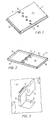
- Fig. 1 there is shown an embodiment of a shield in accordance with the present invention.
- the shield is made from a one piece cover 1 mounted on a printed circuit board 2, e.g. in a mobile telephone or other electronic equipment.
- the cover 1 covers substantially the whole circuit board 2. This is the most space efficient solution since the walls 6 of the cover 1 require space on the circuit board for attachment, e.g. by soldering or gluing. It is also possible that the cover is only covering part of the circuit board, the cover in this case only covering some components and the rest of the circuit board being unshielded or carrying other shields.
- the shields are formed by shielding portions 3 depending from the roof 5, in Figs. 2 and 3 shown as tabs 3 upstanding from the inside of the roof.
- the spacing of the tabs 3 are calculated to get a proper shielding performance.
- the tabs will be located in correct positions relative to the components in question.
- a component may be totally surrounded by shielding walls by placing the tabs in a square around the component.
- the internal shielding walls 3 can be made by cutting out sections from the roof 5 of the cover and bending the section down to form a wall. This will leave openings in the roof, in the embodiment shown as square holes 4. These holes do not pose a problem, but will allow air to circulate inside the cover 1.
- the manufacturing method is especially suitable when using a cover made of a one-piece metal sheet.
- the materials may be manufactured in metallized plastics by injection moulding a plastic shield to a cover having the desired shape and metallizing the cover.
- the cover may be removably attached to the circuit board 2, or permanently fixed by soldering, fusing or gluing etc.
- the present invention has several advantages over the prior art individual shielding cans.
- the shield may be manufactured by means of a simple and cheap metal stamping process.
- the shield saves height because there is only one layer of material.
- the shield provides a very space efficient design of the internal shielding walls, resulting in less waste of PCB area.
Landscapes
- Engineering & Computer Science (AREA)
- Microelectronics & Electronic Packaging (AREA)
- Shielding Devices Or Components To Electric Or Magnetic Fields (AREA)
Priority Applications (6)
| Application Number | Priority Date | Filing Date | Title |
|---|---|---|---|
| EP04445001A EP1515598B1 (de) | 2003-09-12 | 2004-01-02 | Abschirmvorrichtung für eine Leiterplatte und deren Herstellungsverfahren |
| PCT/EP2004/051923 WO2005027610A2 (en) | 2003-09-12 | 2004-08-26 | Shield for circuit board and method of manufacturing same |
| JP2006525811A JP4499724B2 (ja) | 2003-09-12 | 2004-08-26 | 回路基板のシールド及びその製造方法 |
| KR1020067004768A KR20060119940A (ko) | 2003-09-12 | 2004-08-26 | 회로 기판용 실드 및 실드의 제조 방법 |
| TW093125533A TWI340624B (en) | 2003-09-12 | 2004-08-26 | Shield for circuit board and method of manufacturing same |
| BRPI0414233-0A BRPI0414233A (pt) | 2003-09-12 | 2004-08-26 | blindagem para placa de circuito e método de formar a mesma |
Applications Claiming Priority (3)
| Application Number | Priority Date | Filing Date | Title |
|---|---|---|---|
| EP03077870 | 2003-09-12 | ||
| EP03077870 | 2003-09-12 | ||
| EP04445001A EP1515598B1 (de) | 2003-09-12 | 2004-01-02 | Abschirmvorrichtung für eine Leiterplatte und deren Herstellungsverfahren |
Publications (2)
| Publication Number | Publication Date |
|---|---|
| EP1515598A1 true EP1515598A1 (de) | 2005-03-16 |
| EP1515598B1 EP1515598B1 (de) | 2008-09-10 |
Family
ID=34137592
Family Applications (1)
| Application Number | Title | Priority Date | Filing Date |
|---|---|---|---|
| EP04445001A Expired - Lifetime EP1515598B1 (de) | 2003-09-12 | 2004-01-02 | Abschirmvorrichtung für eine Leiterplatte und deren Herstellungsverfahren |
Country Status (2)
| Country | Link |
|---|---|
| EP (1) | EP1515598B1 (de) |
| TW (1) | TWI340624B (de) |
Cited By (1)
| Publication number | Priority date | Publication date | Assignee | Title |
|---|---|---|---|---|
| EP4322720A1 (de) * | 2022-08-09 | 2024-02-14 | Harman International Industries, Inc. | Systeme und verfahren für eine elektronische vorrichtung |
Citations (4)
| Publication number | Priority date | Publication date | Assignee | Title |
|---|---|---|---|---|
| JPH11177270A (ja) * | 1997-12-12 | 1999-07-02 | Mitsumi Electric Co Ltd | 高周波回路装置のアース構造 |
| DE19945427C1 (de) | 1999-09-22 | 2000-11-02 | Siemens Ag | Abschirmvorrichtung und Verfahren zu deren Herstellung |
| WO2002024431A1 (en) | 2000-09-18 | 2002-03-28 | Shielding For Electronics, Inc. | Multi-layered structures and methods for manufacturing the multi-layered structures |
| WO2003032703A1 (en) * | 2001-10-03 | 2003-04-17 | Matsushita Electric Industrial Co., Ltd. | High frequency device |
-
2004
- 2004-01-02 EP EP04445001A patent/EP1515598B1/de not_active Expired - Lifetime
- 2004-08-26 TW TW093125533A patent/TWI340624B/zh not_active IP Right Cessation
Patent Citations (5)
| Publication number | Priority date | Publication date | Assignee | Title |
|---|---|---|---|---|
| JPH11177270A (ja) * | 1997-12-12 | 1999-07-02 | Mitsumi Electric Co Ltd | 高周波回路装置のアース構造 |
| DE19945427C1 (de) | 1999-09-22 | 2000-11-02 | Siemens Ag | Abschirmvorrichtung und Verfahren zu deren Herstellung |
| WO2002024431A1 (en) | 2000-09-18 | 2002-03-28 | Shielding For Electronics, Inc. | Multi-layered structures and methods for manufacturing the multi-layered structures |
| WO2003032703A1 (en) * | 2001-10-03 | 2003-04-17 | Matsushita Electric Industrial Co., Ltd. | High frequency device |
| EP1357779A1 (de) * | 2001-10-03 | 2003-10-29 | Matsushita Electric Industrial Co., Ltd. | Hochfrequenzeinrichtung |
Non-Patent Citations (1)
| Title |
|---|
| PATENT ABSTRACTS OF JAPAN vol. 1999, no. 12 29 October 1999 (1999-10-29) * |
Cited By (2)
| Publication number | Priority date | Publication date | Assignee | Title |
|---|---|---|---|---|
| EP4322720A1 (de) * | 2022-08-09 | 2024-02-14 | Harman International Industries, Inc. | Systeme und verfahren für eine elektronische vorrichtung |
| US12207444B2 (en) | 2022-08-09 | 2025-01-21 | Harman International Industries, Incorporated | Systems and methods for an electronic device |
Also Published As
| Publication number | Publication date |
|---|---|
| TWI340624B (en) | 2011-04-11 |
| TW200511926A (en) | 2005-03-16 |
| EP1515598B1 (de) | 2008-09-10 |
Similar Documents
| Publication | Publication Date | Title |
|---|---|---|
| EP1951021B1 (de) | Abschirmvorrichtung für elektromagnetische Interferenz und Herstellungsverfahren dafür | |
| AU2002250184B2 (en) | Removable electromagnetic interference shield | |
| US7772505B2 (en) | Electromagnetic interference (EMI) shielding apparatus and related methods | |
| US6872880B2 (en) | Two-piece solderless EMC/EMI shield | |
| US20020185294A1 (en) | Push-fit shield and method for fabricating same | |
| US6180876B1 (en) | Apparatus and method for RF shielding of a printed circuit board | |
| US20020106939A1 (en) | Control device and soldering method | |
| GB2297868A (en) | EMI/RFI shielding device | |
| CN101278608A (zh) | 电磁干扰屏蔽装置及相关制造方法 | |
| US7442881B1 (en) | Shielding device | |
| EP0702512B1 (de) | Abschirmungsvorrichtung und Verfahren zur Montage | |
| EP0726700A1 (de) | Abschirmungsvorrichtung | |
| US7087835B2 (en) | Apparatus and method for shielding printed circuit boards | |
| EP1515598B1 (de) | Abschirmvorrichtung für eine Leiterplatte und deren Herstellungsverfahren | |
| US5946199A (en) | Shielding case | |
| US20040057198A1 (en) | Device housing comprising an electromagnetically shielded region | |
| WO2005027610A2 (en) | Shield for circuit board and method of manufacturing same | |
| US20070121309A1 (en) | Shielding device | |
| US20180168077A1 (en) | Two-Piece Solderable Shield | |
| US20050185383A1 (en) | Power amplifier module assembly | |
| JPH06338695A (ja) | シールドケース | |
| EP1121006B1 (de) | Sende-Empfangseinheit zur Sicherstellung der Montage einer Abdeckung auf einem Metallrahmen | |
| JP2009158586A (ja) | 高周波回路ユニット | |
| EP1981323A2 (de) | Vorrichtung zur elektromagnetischen Abschirmung | |
| CN1849859A (zh) | 用于电路板的屏蔽罩及制造该屏蔽罩的方法 |
Legal Events
| Date | Code | Title | Description |
|---|---|---|---|
| PUAI | Public reference made under article 153(3) epc to a published international application that has entered the european phase |
Free format text: ORIGINAL CODE: 0009012 |
|
| AK | Designated contracting states |
Kind code of ref document: A1 Designated state(s): AT BE BG CH CY CZ DE DK EE ES FI FR GB GR HU IE IT LI LU MC NL PT RO SE SI SK TR |
|
| AX | Request for extension of the european patent |
Extension state: AL LT LV MK |
|
| 17P | Request for examination filed |
Effective date: 20050820 |
|
| AKX | Designation fees paid |
Designated state(s): AT BE BG CH CY CZ DE DK EE ES FI FR GB GR HU IE IT LI LU MC NL PT RO SE SI SK TR |
|
| 17Q | First examination report despatched |
Effective date: 20071005 |
|
| GRAP | Despatch of communication of intention to grant a patent |
Free format text: ORIGINAL CODE: EPIDOSNIGR1 |
|
| GRAS | Grant fee paid |
Free format text: ORIGINAL CODE: EPIDOSNIGR3 |
|
| GRAA | (expected) grant |
Free format text: ORIGINAL CODE: 0009210 |
|
| AK | Designated contracting states |
Kind code of ref document: B1 Designated state(s): AT BE BG CH CY CZ DE DK EE ES FI FR GB GR HU IE IT LI LU MC NL PT RO SE SI SK TR |
|
| REG | Reference to a national code |
Ref country code: GB Ref legal event code: FG4D |
|
| REG | Reference to a national code |
Ref country code: CH Ref legal event code: EP |
|
| REG | Reference to a national code |
Ref country code: IE Ref legal event code: FG4D |
|
| REF | Corresponds to: |
Ref document number: 602004016434 Country of ref document: DE Date of ref document: 20081023 Kind code of ref document: P |
|
| PG25 | Lapsed in a contracting state [announced via postgrant information from national office to epo] |
Ref country code: SI Free format text: LAPSE BECAUSE OF FAILURE TO SUBMIT A TRANSLATION OF THE DESCRIPTION OR TO PAY THE FEE WITHIN THE PRESCRIBED TIME-LIMIT Effective date: 20080910 Ref country code: AT Free format text: LAPSE BECAUSE OF FAILURE TO SUBMIT A TRANSLATION OF THE DESCRIPTION OR TO PAY THE FEE WITHIN THE PRESCRIBED TIME-LIMIT Effective date: 20080910 Ref country code: FI Free format text: LAPSE BECAUSE OF FAILURE TO SUBMIT A TRANSLATION OF THE DESCRIPTION OR TO PAY THE FEE WITHIN THE PRESCRIBED TIME-LIMIT Effective date: 20080910 |
|
| NLV1 | Nl: lapsed or annulled due to failure to fulfill the requirements of art. 29p and 29m of the patents act | ||
| PG25 | Lapsed in a contracting state [announced via postgrant information from national office to epo] |
Ref country code: BE Free format text: LAPSE BECAUSE OF FAILURE TO SUBMIT A TRANSLATION OF THE DESCRIPTION OR TO PAY THE FEE WITHIN THE PRESCRIBED TIME-LIMIT Effective date: 20080910 |
|
| PG25 | Lapsed in a contracting state [announced via postgrant information from national office to epo] |
Ref country code: ES Free format text: LAPSE BECAUSE OF FAILURE TO SUBMIT A TRANSLATION OF THE DESCRIPTION OR TO PAY THE FEE WITHIN THE PRESCRIBED TIME-LIMIT Effective date: 20081221 Ref country code: BG Free format text: LAPSE BECAUSE OF FAILURE TO SUBMIT A TRANSLATION OF THE DESCRIPTION OR TO PAY THE FEE WITHIN THE PRESCRIBED TIME-LIMIT Effective date: 20081210 |
|
| PG25 | Lapsed in a contracting state [announced via postgrant information from national office to epo] |
Ref country code: SK Free format text: LAPSE BECAUSE OF FAILURE TO SUBMIT A TRANSLATION OF THE DESCRIPTION OR TO PAY THE FEE WITHIN THE PRESCRIBED TIME-LIMIT Effective date: 20080910 Ref country code: RO Free format text: LAPSE BECAUSE OF FAILURE TO SUBMIT A TRANSLATION OF THE DESCRIPTION OR TO PAY THE FEE WITHIN THE PRESCRIBED TIME-LIMIT Effective date: 20080910 Ref country code: PT Free format text: LAPSE BECAUSE OF FAILURE TO SUBMIT A TRANSLATION OF THE DESCRIPTION OR TO PAY THE FEE WITHIN THE PRESCRIBED TIME-LIMIT Effective date: 20090210 Ref country code: CZ Free format text: LAPSE BECAUSE OF FAILURE TO SUBMIT A TRANSLATION OF THE DESCRIPTION OR TO PAY THE FEE WITHIN THE PRESCRIBED TIME-LIMIT Effective date: 20080910 Ref country code: NL Free format text: LAPSE BECAUSE OF FAILURE TO SUBMIT A TRANSLATION OF THE DESCRIPTION OR TO PAY THE FEE WITHIN THE PRESCRIBED TIME-LIMIT Effective date: 20080910 |
|
| PLBE | No opposition filed within time limit |
Free format text: ORIGINAL CODE: 0009261 |
|
| STAA | Information on the status of an ep patent application or granted ep patent |
Free format text: STATUS: NO OPPOSITION FILED WITHIN TIME LIMIT |
|
| PG25 | Lapsed in a contracting state [announced via postgrant information from national office to epo] |
Ref country code: DK Free format text: LAPSE BECAUSE OF FAILURE TO SUBMIT A TRANSLATION OF THE DESCRIPTION OR TO PAY THE FEE WITHIN THE PRESCRIBED TIME-LIMIT Effective date: 20080910 Ref country code: EE Free format text: LAPSE BECAUSE OF FAILURE TO SUBMIT A TRANSLATION OF THE DESCRIPTION OR TO PAY THE FEE WITHIN THE PRESCRIBED TIME-LIMIT Effective date: 20080910 |
|
| 26N | No opposition filed |
Effective date: 20090611 |
|
| PG25 | Lapsed in a contracting state [announced via postgrant information from national office to epo] |
Ref country code: IT Free format text: LAPSE BECAUSE OF FAILURE TO SUBMIT A TRANSLATION OF THE DESCRIPTION OR TO PAY THE FEE WITHIN THE PRESCRIBED TIME-LIMIT Effective date: 20080910 Ref country code: MC Free format text: LAPSE BECAUSE OF NON-PAYMENT OF DUE FEES Effective date: 20090131 |
|
| REG | Reference to a national code |
Ref country code: CH Ref legal event code: PL |
|
| PG25 | Lapsed in a contracting state [announced via postgrant information from national office to epo] |
Ref country code: CH Free format text: LAPSE BECAUSE OF NON-PAYMENT OF DUE FEES Effective date: 20090131 Ref country code: LI Free format text: LAPSE BECAUSE OF NON-PAYMENT OF DUE FEES Effective date: 20090131 |
|
| PG25 | Lapsed in a contracting state [announced via postgrant information from national office to epo] |
Ref country code: IE Free format text: LAPSE BECAUSE OF NON-PAYMENT OF DUE FEES Effective date: 20090102 Ref country code: SE Free format text: LAPSE BECAUSE OF FAILURE TO SUBMIT A TRANSLATION OF THE DESCRIPTION OR TO PAY THE FEE WITHIN THE PRESCRIBED TIME-LIMIT Effective date: 20081210 |
|
| PG25 | Lapsed in a contracting state [announced via postgrant information from national office to epo] |
Ref country code: GR Free format text: LAPSE BECAUSE OF FAILURE TO SUBMIT A TRANSLATION OF THE DESCRIPTION OR TO PAY THE FEE WITHIN THE PRESCRIBED TIME-LIMIT Effective date: 20081211 |
|
| PG25 | Lapsed in a contracting state [announced via postgrant information from national office to epo] |
Ref country code: LU Free format text: LAPSE BECAUSE OF NON-PAYMENT OF DUE FEES Effective date: 20090102 |
|
| PG25 | Lapsed in a contracting state [announced via postgrant information from national office to epo] |
Ref country code: HU Free format text: LAPSE BECAUSE OF FAILURE TO SUBMIT A TRANSLATION OF THE DESCRIPTION OR TO PAY THE FEE WITHIN THE PRESCRIBED TIME-LIMIT Effective date: 20090311 |
|
| PG25 | Lapsed in a contracting state [announced via postgrant information from national office to epo] |
Ref country code: TR Free format text: LAPSE BECAUSE OF FAILURE TO SUBMIT A TRANSLATION OF THE DESCRIPTION OR TO PAY THE FEE WITHIN THE PRESCRIBED TIME-LIMIT Effective date: 20080910 |
|
| PG25 | Lapsed in a contracting state [announced via postgrant information from national office to epo] |
Ref country code: CY Free format text: LAPSE BECAUSE OF FAILURE TO SUBMIT A TRANSLATION OF THE DESCRIPTION OR TO PAY THE FEE WITHIN THE PRESCRIBED TIME-LIMIT Effective date: 20080910 |
|
| REG | Reference to a national code |
Ref country code: FR Ref legal event code: PLFP Year of fee payment: 12 |
|
| PGFP | Annual fee paid to national office [announced via postgrant information from national office to epo] |
Ref country code: GB Payment date: 20141231 Year of fee payment: 12 |
|
| PGFP | Annual fee paid to national office [announced via postgrant information from national office to epo] |
Ref country code: DE Payment date: 20141231 Year of fee payment: 12 |
|
| PGFP | Annual fee paid to national office [announced via postgrant information from national office to epo] |
Ref country code: FR Payment date: 20150108 Year of fee payment: 12 |
|
| REG | Reference to a national code |
Ref country code: DE Ref legal event code: R119 Ref document number: 602004016434 Country of ref document: DE |
|
| GBPC | Gb: european patent ceased through non-payment of renewal fee |
Effective date: 20160102 |
|
| REG | Reference to a national code |
Ref country code: FR Ref legal event code: ST Effective date: 20160930 |
|
| PG25 | Lapsed in a contracting state [announced via postgrant information from national office to epo] |
Ref country code: DE Free format text: LAPSE BECAUSE OF NON-PAYMENT OF DUE FEES Effective date: 20160802 Ref country code: GB Free format text: LAPSE BECAUSE OF NON-PAYMENT OF DUE FEES Effective date: 20160102 |
|
| PG25 | Lapsed in a contracting state [announced via postgrant information from national office to epo] |
Ref country code: FR Free format text: LAPSE BECAUSE OF NON-PAYMENT OF DUE FEES Effective date: 20160201 |