EP1513384A2 - Electronic circuit unit having small size and good productivity - Google Patents
Electronic circuit unit having small size and good productivity Download PDFInfo
- Publication number
- EP1513384A2 EP1513384A2 EP04020884A EP04020884A EP1513384A2 EP 1513384 A2 EP1513384 A2 EP 1513384A2 EP 04020884 A EP04020884 A EP 04020884A EP 04020884 A EP04020884 A EP 04020884A EP 1513384 A2 EP1513384 A2 EP 1513384A2
- Authority
- EP
- European Patent Office
- Prior art keywords
- circuit board
- terminal group
- cover
- circuit unit
- terminals
- Prior art date
- Legal status (The legal status is an assumption and is not a legal conclusion. Google has not performed a legal analysis and makes no representation as to the accuracy of the status listed.)
- Withdrawn
Links
Images
Classifications
-
- H—ELECTRICITY
- H05—ELECTRIC TECHNIQUES NOT OTHERWISE PROVIDED FOR
- H05K—PRINTED CIRCUITS; CASINGS OR CONSTRUCTIONAL DETAILS OF ELECTRIC APPARATUS; MANUFACTURE OF ASSEMBLAGES OF ELECTRICAL COMPONENTS
- H05K9/00—Screening of apparatus or components against electric or magnetic fields
- H05K9/0007—Casings
- H05K9/002—Casings with localised screening
-
- H—ELECTRICITY
- H05—ELECTRIC TECHNIQUES NOT OTHERWISE PROVIDED FOR
- H05K—PRINTED CIRCUITS; CASINGS OR CONSTRUCTIONAL DETAILS OF ELECTRIC APPARATUS; MANUFACTURE OF ASSEMBLAGES OF ELECTRICAL COMPONENTS
- H05K7/00—Constructional details common to different types of electric apparatus
- H05K7/02—Arrangements of circuit components or wiring on supporting structure
- H05K7/04—Arrangements of circuit components or wiring on supporting structure on conductive chassis
-
- H—ELECTRICITY
- H05—ELECTRIC TECHNIQUES NOT OTHERWISE PROVIDED FOR
- H05K—PRINTED CIRCUITS; CASINGS OR CONSTRUCTIONAL DETAILS OF ELECTRIC APPARATUS; MANUFACTURE OF ASSEMBLAGES OF ELECTRICAL COMPONENTS
- H05K1/00—Printed circuits
- H05K1/18—Printed circuits structurally associated with non-printed electric components
-
- H—ELECTRICITY
- H05—ELECTRIC TECHNIQUES NOT OTHERWISE PROVIDED FOR
- H05K—PRINTED CIRCUITS; CASINGS OR CONSTRUCTIONAL DETAILS OF ELECTRIC APPARATUS; MANUFACTURE OF ASSEMBLAGES OF ELECTRICAL COMPONENTS
- H05K7/00—Constructional details common to different types of electric apparatus
- H05K7/14—Mounting supporting structure in casing or on frame or rack
-
- H—ELECTRICITY
- H05—ELECTRIC TECHNIQUES NOT OTHERWISE PROVIDED FOR
- H05K—PRINTED CIRCUITS; CASINGS OR CONSTRUCTIONAL DETAILS OF ELECTRIC APPARATUS; MANUFACTURE OF ASSEMBLAGES OF ELECTRICAL COMPONENTS
- H05K1/00—Printed circuits
- H05K1/02—Details
- H05K1/0213—Electrical arrangements not otherwise provided for
- H05K1/0237—High frequency adaptations
- H05K1/0243—Printed circuits associated with mounted high frequency components
-
- H—ELECTRICITY
- H05—ELECTRIC TECHNIQUES NOT OTHERWISE PROVIDED FOR
- H05K—PRINTED CIRCUITS; CASINGS OR CONSTRUCTIONAL DETAILS OF ELECTRIC APPARATUS; MANUFACTURE OF ASSEMBLAGES OF ELECTRICAL COMPONENTS
- H05K2201/00—Indexing scheme relating to printed circuits covered by H05K1/00
- H05K2201/10—Details of components or other objects attached to or integrated in a printed circuit board
- H05K2201/10007—Types of components
- H05K2201/10075—Non-printed oscillator
-
- H—ELECTRICITY
- H05—ELECTRIC TECHNIQUES NOT OTHERWISE PROVIDED FOR
- H05K—PRINTED CIRCUITS; CASINGS OR CONSTRUCTIONAL DETAILS OF ELECTRIC APPARATUS; MANUFACTURE OF ASSEMBLAGES OF ELECTRICAL COMPONENTS
- H05K2201/00—Indexing scheme relating to printed circuits covered by H05K1/00
- H05K2201/10—Details of components or other objects attached to or integrated in a printed circuit board
- H05K2201/10007—Types of components
- H05K2201/10189—Non-printed connector
-
- H—ELECTRICITY
- H05—ELECTRIC TECHNIQUES NOT OTHERWISE PROVIDED FOR
- H05K—PRINTED CIRCUITS; CASINGS OR CONSTRUCTIONAL DETAILS OF ELECTRIC APPARATUS; MANUFACTURE OF ASSEMBLAGES OF ELECTRICAL COMPONENTS
- H05K2201/00—Indexing scheme relating to printed circuits covered by H05K1/00
- H05K2201/10—Details of components or other objects attached to or integrated in a printed circuit board
- H05K2201/10431—Details of mounted components
- H05K2201/10439—Position of a single component
- H05K2201/10446—Mounted on an edge
-
- H—ELECTRICITY
- H05—ELECTRIC TECHNIQUES NOT OTHERWISE PROVIDED FOR
- H05K—PRINTED CIRCUITS; CASINGS OR CONSTRUCTIONAL DETAILS OF ELECTRIC APPARATUS; MANUFACTURE OF ASSEMBLAGES OF ELECTRICAL COMPONENTS
- H05K2201/00—Indexing scheme relating to printed circuits covered by H05K1/00
- H05K2201/20—Details of printed circuits not provided for in H05K2201/01 - H05K2201/10
- H05K2201/2018—Presence of a frame in a printed circuit or printed circuit assembly
Definitions
- the present invention relates to an electronic circuit unit suitable for a television tuner and the like.
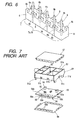
- Fig. 7 is an exploded perspective view of a conventional electronic circuit unit.
- a box-shaped (a square shape) frame member 51 composed of a metal plate has opened portions 51a and 51b provided in two of its sides, tongue pieces 51c respectively provided in four sides of the square shape, and a plurality of mounting legs 51d projecting downward from the vicinities of four corners.
- a shield plate 52 composed of a metal plate is arranged within the frame member 51 to divide the inside of the frame member 51 into a plurality of divided rooms.
- a circuit board 53 composed of an insulating substrate has a plurality of notched portions 53a provided in its outer circumferential edge, and a conductive pattern (not shown) for wiring lines is provided on front and rear surfaces of the circuit board.
- a plurality of linear terminals 56 is arranged to pass through the circuit board 53 in the vicinity of one side of the circuit board 53 and is mounted in the conductive pattern by means of solder.
- the plurality of terminals 56 is arranged at equal intervals in a line. As regards the respective terminals, a portion projecting downward from the circuit board 53 is a terminal portion 56a, and a portion projecting upward from the circuit board 53 is a retaining portion 56b.
- circuit board 53 is housed in the frame member 51, and the tongue pieces 51c are bent toward the notched portions 53a.
- the conductive pattern and the tongue pieces 51c are soldered, whereby the circuit board 53 is mounted in the frame member 51.
- a first cover (an upper cover) 57 and a second cover (a lower cover) 58 composed of a metal plate are respectively mounted in the frame member 51 so as to cover the opened portions 51a and 51b of the frame member 51.
- the plurality of terminals 56 is arranged in a line, and the electronic component with the cover 54 is arranged out of line. Therefore, the size of the circuit board 53 increases in a widthwise direction.
- the manufacturing workability is generally decreased.
- an electronic circuit unit comprising: a box-shaped frame member composed of a metal plate; a circuit board mounted in the frame member; an electronic component with a cover mounted on the circuit board; and a plurality of linear terminals mounted in the circuit board while passing through the circuit board, wherein the terminals comprise at least a first terminal group and a second terminal group arranged at an interval between the respective terminals in a line, the first terminal group and the second terminal group being arranged in the vicinity of one side of the circuit board, wherein an opening portion is provided between the first terminal group and the second terminal group, and wherein the electronic component with the cover is mounted on the circuit board while being disposed in the opening portion.
- the electronic component comprises a quartz oscillator.
- the electronic circuit unit further comprises supporting members made of an insulating material, wherein one end of each of the terminals is supported by the supporting member, and the supporting members and the electronic component with the cover are arranged on the same surface of the circuit board.
- the supporting members are integrally formed with the first terminal group and the second terminal group, respectively.
- the inside of the frame member is divided into a plurality of divided rooms by means of a shield plate, wherein a tuner circuit portion for frequency-converting received television signals into intermediate frequency signals and a demodulation circuit portion for detecting the intermediate frequency signals and for outputting video signals and audio signals are respectively arranged in the divided rooms adjacent to each other with the shield plate interposed therebetween, and wherein a phase locked loop (PLL) IC provided in the tuner circuit portion and a demodulation IC provided in the demodulation circuit portion are connected to the quartz oscillator.
- PLL phase locked loop
- the quartz oscillator is housed in the divided room disposed at the side of the tuner circuit portion adjacent to the shield plate provided between the tuner circuit portion and the demodulation circuit portion.
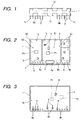
- Fig. 1 is a front view showing an electronic circuit unit of the present invention.
- Fig. 2 is a plan view of the electronic circuit unit of the present invention in a state in which a cover is removed.
- Fig. 3 is a bottom view of the electronic circuit unit of the present invention in a state in which a cover is removed.
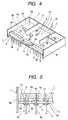
- Fig. 4 is a perspective view of the electronic circuit unit of the present invention with the cover removed in which a portion thereof is cut out.
- Fig. 5 is an enlarged cross-sectional view of essential parts of the electronic circuit unit of the present invention.
- Fig. 6 is a perspective view of the electronic circuit unit of the present invention in a state in which a terminal member is turned over.
- the electronic circuit unit has a box-shaped (a square shape) frame member 1 composed of a metal plate, opened portions 1a and 1b provided in two of its sides, and a plurality of mounting legs 1c projecting downward from the vicinities of four corners.
- a box-shaped (a square shape) frame member 1 composed of a metal plate, opened portions 1a and 1b provided in two of its sides, and a plurality of mounting legs 1c projecting downward from the vicinities of four corners.
- a shield plate 2 composed of a metal plate is arranged within the frame member 1 to divide the inside of the frame member 1 into a plurality of divided rooms S1 and S2.
- a conductive pattern 4 for wiring lines is provided on the front and rear surfaces of a rectangular circuit board 3 composed of a ceramic substrate, and a conductive pattern 4 for wiring lines is provided, and an electronic component 5 with a metal cover, such as a quartz oscillator, electronic components 6, such as a PLL IC P1, a demodulation IC P2, a coil, and a chip resistor, are mounted on the circuit board 3, thereby forming a desired electric circuit.
- a metal cover such as a quartz oscillator
- electronic components 6 such as a PLL IC P1, a demodulation IC P2, a coil, and a chip resistor
- a tuner circuit portion K1 for frequency-converting received television signals into intermediate frequency signals and a demodulation circuit portion K2 for detecting the intermediate frequency signals and for outputting video signals and audio signals are provided on the circuit board 3, and the tuner circuit portion K1 and the demodulation circuit portion K2 are respectively arranged in the divided rooms S1 and S2 adjacent to each other with the shield plate 2 interposed therebetween.
- the PLL IC P1 is provided in the tuner circuit portion K1
- the demodulation IC P2 is provided in the demodulation circuit portion K2.
- the electronic component 5 with the cover which is a quartz oscillator, is connected to the PLL IC P1 and the demodulation IC P2.
- the electronic component 5 with the cover which is a quartz oscillator, is housed in the divided room S1 disposed at the side of the tuner circuit portion K1 adjacent to the shield plate 2 provided between the tuner circuit portion K1 and the demodulation circuit portion K2, it is possible to connect the electronic component 5 with the cover to the PLL IC P1 and the demodulation IC P2 at a short distance.
- terminal members 7 comprises a plurality of supporting members 8 made of an insulating material, such as a ceramic material, and a plurality of terminals 9 each made of a metallic line (a linear shape).
- the plurality of supporting members 8 is integrally formed in a line, and one end portion 9a of each of the plurality of terminals 9 is buried at the lower center of each supporting member 8 to be supported. In addition, a terminal portion 9b of the other end thereof projects downward.
- the supporting members 8 each have cross-shaped cavity portions 8a provided in the vicinities of the terminals 9, projections 8b projecting downward to form the cavity portions 8a, and slits 8c provided in the outer circumferences between adjacent supporting members 8.
- the cavity portions 8a are formed in a cross shape, but may be formed in a circular shape or a rectangular shape.
- the terminal members 7 have a plurality of supporting members 8 (in the present embodiment, five supporting members), and a first terminal group 7a and a second terminal group 7b, each comprising a plurality of terminals 9 (in the present embodiment, five terminals) respectively mounted in the supporting members 8.
- the first terminal group 7a and the second terminal group 7b are respectively manufactured by burying (mounting) a number of terminals 9 in a line, and by cutting along the slit 8c at a position of the desired number of the supporting members 8 in a state in which a number of supporting members 8 are integrated in a line.
- first terminal group 7a and the second terminal group 7b having such a construction are arranged in the vicinity of one side of the circuit board 3 in a line, and an opening portion 10 is provided between the first terminal group 7a and the second terminal group 7b.
- the projections 8b of the supporting members 8 come in contact with an upper surface of the circuit board 3, and the terminal portions 9b pass through holes 3a of the circuit board 3 to project downward.
- the cavity portions 8a exist in the vicinities of the terminals 9 disposed at the upper surface of the circuit board 3.
- terminal portions 9b of the terminals 9 are respectively connected and fixed to the conductive patterns 4 provided in a lower surface of the circuit board 3 by means of solder 11.
- soldering method of the solder first, in a state in which solder cream (not shown) is coated on the conductive patterns 4 of the lower surface of the circuit board 3, the terminals 9 of the first and second terminal groups 7a and 7b are allowed to pass through the holes 3a from the upper surface of the circuit board 3.
- the circuit board 3 is conveyed into a reflow furnace as it is, and the soldering of the solder 11 is performed by melting the solder cream. At this time, the melted solder 11 flows out toward the upper surface of the circuit board 3 via the holes 3a by means of a capillary phenomenon.
- the solder 11 flown out on the upper surface of the circuit board 3 is located within the cavity portions 8a, it is possible to prevent the supporting members 8 from being lifted (a floated state) by the solder 11 flown out on the upper surface, thereby precisely mounting the terminal members 7.
- the plurality of supporting members 8 is integrally formed, but a plurality of supporting members 8 may be separately arranged in a line.
- the above-mentioned electronic component 5 with the cover has a cover 5a with a flange for covering a main body portion and leads (terminals) 5b projecting downward from the main body portion.
- the leads 5b pass through the holes 3a and are connected to the conductive patterns 4 provided in the lower surface of the circuit board 3 by means of solder.
- a soldering method of the electronic component 5 with the cover is similar to the soldering method of the terminal members 7 described above, and the soldering of the electronic component 5 with the cover and the terminal members 7 is simultaneously performed after being conveyed into the reflow furnace.
- the electronic component 5 with the cover is arranged in the opening portion 10, such that it is possible to reduce a widthwise dimension of the circuit board 3. Further, since the supporting members 8 of the terminal members 7, which are made of an insulating material, are positioned in the vicinity of the cover 5a, it is possible to more reliably insulate the cover 5a from the terminals 9.
- circuit board 3 is housed in the frame member 1, and is mounted in the frame member 1 by means of appropriate means.
- the electronic component 5 with the cover is housed in the divided room S1 in which the tuner circuit portion K1 is provided at a position between the first and second terminal groups 7a and 7b.
- the first cover (the upper cover) 12 and the second cover (the lower cover) 13 that are composed of a metal plate are respectively mounted in the frame member 1 while covering the opened portions 1a and 1b of the frame member 1.
- terminal portions 9b of the terminals 9 project downward from the holes of the second cover 13, which are not shown in the drawings.
- the electronic circuit unit of the present invention comprises a box-shaped frame member composed of a metal plate, a circuit board mounted in the frame member, an electronic component with a cover mounted on the circuit board, and a plurality of linear terminals mounted in the circuit board while passing through the circuit board, wherein the terminals comprise at least a first terminal group and a second terminal group arranged at an interval between the respective terminals in a line, the first terminal group and the second terminal group being arranged in the vicinity of one side of the circuit board, wherein an opening portion is provided between the first terminal group and the second terminal group, and wherein the electronic component with the cover is mounted on the circuit board while being disposed in the opening portion.
- a good space factor for the arrangement of the electronic component with the cover can be obtained, such that it is possible to reduce a widthwise direction dimension of the circuit board, thereby obtaining a small-sized electronic circuit unit.
- the electronic circuit unit of the present invention is suitable for, in particular, a television tuner device.
- the electronic circuit unit further comprises supporting members made of an insulating material, one end of each of the respective terminals is supported by the supporting member, and the supporting members and the electronic component with the cover are arranged on the same surface of the circuit board. Therefore, it is possible to more reliably insulate the electronic component with the cover from the terminals.
- the supporting members are integrally formed with the first terminal group and the second terminal group, respectively, it is easier to mount the terminals on the circuit board, and thus it is possible to obtain an electronic circuit unit having a good manufacturing productivity.
- the inside of the frame member is divided into a plurality of divided rooms by means of a shield plate, and a tuner circuit portion for frequency-converting received television signals into intermediate frequency signals and a demodulation circuit portion for detecting the intermediate frequency signals and for outputting video signals and audio signals are respectively arranged in the divided rooms adjacent to each other with the shield plate interposed therebetween.
- a phase locked loop (PLL) IC provided in the tuner circuit portion and a demodulation IC provided in the demodulation circuit portion are connected to the quartz oscillator.
- PLL phase locked loop
- the quartz oscillator is housed in the divided room disposed at the side of the tuner circuit portion adjacent to the shield plate provided between the tuner circuit portion and the demodulation circuit portion, it is possible to connect the quart oscillator to the PLL IC and the demodulation IC at a short distance.
Landscapes
- Engineering & Computer Science (AREA)
- Microelectronics & Electronic Packaging (AREA)
- Shielding Devices Or Components To Electric Or Magnetic Fields (AREA)
- Structure Of Receivers (AREA)
- Casings For Electric Apparatus (AREA)
- Structures For Mounting Electric Components On Printed Circuit Boards (AREA)
- Oscillators With Electromechanical Resonators (AREA)
- Combinations Of Printed Boards (AREA)
Abstract
Description
Claims (6)
- An electronic circuit unit comprising:wherein the terminals comprise at least a first terminal group and a second terminal group arranged at an interval between the respective terminals in a line, the first terminal group and the second terminal group being arranged in the vicinity of one side of the circuit board,a box-shaped frame member composed of a metal plate;a circuit board mounted in the frame member;an electronic component with a cover mounted on the circuit board; anda plurality of linear terminals that passes through and is mounted in the circuit board,
wherein an opening portion is provided between the first terminal group and the second terminal group, and
wherein the electronic component with the cover is mounted on the circuit board while being disposed in the opening portion. - The electronic circuit unit according to claim 1,
wherein the electronic component with the cover comprises a quartz oscillator. - The electronic circuit unit according to claim 1 or 2, further comprising supporting members made of an insulating material,
wherein one end of each of the terminals is supported by the supporting member, and the supporting members and the electronic component with the cover are arranged on the same surface of the circuit board. - The electronic circuit unit according to claim 3,
wherein the supporting members are integrally formed with the first terminal group and the second terminal group, respectively. - The electronic circuit unit according to any of claims 2 to 4,
wherein the inside of the frame member is divided into a plurality of divided rooms by means of a shield plate,
wherein a tuner circuit portion for frequency-converting received television signals into intermediate frequency signals and a demodulation circuit portion for detecting the intermediate frequency signals and for outputting video signals and audio signals are respectively arranged in the divided rooms adjacent to each other with the shield plate interposed therebetween, and
wherein a phase locked loop (PLL) IC provided in the tuner circuit portion and a demodulation IC provided in the demodulation circuit portion are connected to the quartz oscillator. - The electronic circuit unit according to claim 5,
wherein the quartz oscillator is housed in the divided room disposed at the side of the tuner circuit portion adjacent to the shield plate provided between the tuner circuit portion and the demodulation circuit portion.
Applications Claiming Priority (2)
| Application Number | Priority Date | Filing Date | Title |
|---|---|---|---|
| JP2003313910A JP4170862B2 (en) | 2003-09-05 | 2003-09-05 | Electronic circuit unit |
| JP2003313910 | 2003-09-05 |
Publications (2)
| Publication Number | Publication Date |
|---|---|
| EP1513384A2 true EP1513384A2 (en) | 2005-03-09 |
| EP1513384A3 EP1513384A3 (en) | 2008-12-31 |
Family
ID=34131897
Family Applications (1)
| Application Number | Title | Priority Date | Filing Date |
|---|---|---|---|
| EP04020884A Withdrawn EP1513384A3 (en) | 2003-09-05 | 2004-09-02 | Electronic circuit unit having small size and good productivity |
Country Status (5)
| Country | Link |
|---|---|
| US (1) | US7106085B2 (en) |
| EP (1) | EP1513384A3 (en) |
| JP (1) | JP4170862B2 (en) |
| KR (1) | KR100586902B1 (en) |
| CN (1) | CN100379326C (en) |
Families Citing this family (7)
| Publication number | Priority date | Publication date | Assignee | Title |
|---|---|---|---|---|
| JP2006311161A (en) * | 2005-04-28 | 2006-11-09 | Denso Corp | Wireless transceiver and method for manufacturing wireless transceiver |
| KR100716826B1 (en) * | 2005-05-10 | 2007-05-09 | 삼성전기주식회사 | Manufacturing Method of Board with Electronic Component |
| JP2007267172A (en) | 2006-03-29 | 2007-10-11 | Alps Electric Co Ltd | Tuner for digital broadcasting, and digital broadcast receiving apparatus using same |
| KR100829755B1 (en) | 2007-03-02 | 2008-05-15 | 삼성에스디아이 주식회사 | Chassis Base Assembly and Display Device Having Same |
| US8484905B2 (en) * | 2008-07-15 | 2013-07-16 | Siemens Aktiengesellschaft | Tower and method for the assembly of a tower |
| TWM429683U (en) * | 2012-01-06 | 2012-05-21 | Bothhand Entpr Inc | Packaging case of electronic device |
| JP5984526B2 (en) | 2012-06-20 | 2016-09-06 | 日本電波工業株式会社 | Surface mount device |
Family Cites Families (21)
| Publication number | Priority date | Publication date | Assignee | Title |
|---|---|---|---|---|
| US4306205A (en) * | 1978-10-31 | 1981-12-15 | Murata Manufacturing Co., Ltd. | High frequency apparatus |
| CH687276A5 (en) * | 1989-01-23 | 1996-10-31 | Balzers Hochvakuum | Tuning fork quartz manometer. |
| JP3176963B2 (en) * | 1991-08-30 | 2001-06-18 | 新潟精密株式会社 | High frequency clock circuit |
| JPH08222827A (en) * | 1995-02-14 | 1996-08-30 | Daishinku Co | Insulation plate for electronic parts |
| JP3825475B2 (en) * | 1995-06-30 | 2006-09-27 | 株式会社 東芝 | Manufacturing method of electronic parts |
| DE19636181A1 (en) * | 1996-09-06 | 1998-03-12 | Philips Patentverwaltung | RF module, e.g. B. Tuner |
| JP3333811B2 (en) * | 1996-10-25 | 2002-10-15 | アルプス電気株式会社 | Manufacturing method of high frequency equipment |
| JP3179719B2 (en) * | 1996-11-20 | 2001-06-25 | アルプス電気株式会社 | Electronics |
| JPH11136152A (en) * | 1997-10-31 | 1999-05-21 | Alps Electric Co Ltd | Digital television signal reception tuner |
| JP4379932B2 (en) * | 1998-09-18 | 2009-12-09 | エプソントヨコム株式会社 | Crystal oscillator |
| JP2000165086A (en) * | 1998-11-30 | 2000-06-16 | Kinseki Ltd | Electronic parts container |
| JP3062909U (en) * | 1999-04-08 | 1999-10-15 | 船井電機株式会社 | Tuner unit |
| JP2001177044A (en) * | 1999-12-15 | 2001-06-29 | Murata Mfg Co Ltd | Electronic part module and piezoelectric oscillator |
| JP3729708B2 (en) | 2000-06-19 | 2005-12-21 | シャープ株式会社 | Electronics |
| JP4701505B2 (en) * | 2001-01-29 | 2011-06-15 | パナソニック株式会社 | Inertial transducer |
| US6774641B2 (en) * | 2001-06-20 | 2004-08-10 | Nec Corporation | Printed circuit board design support apparatus, method, and program |
| JP2003218259A (en) * | 2002-01-28 | 2003-07-31 | Tokyo Denpa Co Ltd | Electronic component container |
| US6846998B2 (en) * | 2002-01-28 | 2005-01-25 | Citizen Watch Co., Ltd. | Switch connecting structure for timepiece |
| JP4051321B2 (en) * | 2002-06-27 | 2008-02-20 | 京セラ株式会社 | Manufacturing method of electronic component device |
| JP2004312285A (en) * | 2003-04-04 | 2004-11-04 | Toyo Commun Equip Co Ltd | Surface mount type piezoelectric oscillator |
| JP2005235806A (en) * | 2004-02-17 | 2005-09-02 | Toyo Commun Equip Co Ltd | Electronic parts with case |
-
2003
- 2003-09-05 JP JP2003313910A patent/JP4170862B2/en not_active Expired - Fee Related
-
2004
- 2004-07-23 KR KR1020040057457A patent/KR100586902B1/en not_active Expired - Fee Related
- 2004-09-02 US US10/932,953 patent/US7106085B2/en not_active Expired - Fee Related
- 2004-09-02 EP EP04020884A patent/EP1513384A3/en not_active Withdrawn
- 2004-09-06 CN CNB2004100687316A patent/CN100379326C/en not_active Expired - Fee Related
Also Published As
| Publication number | Publication date |
|---|---|
| CN1592558A (en) | 2005-03-09 |
| JP2005085863A (en) | 2005-03-31 |
| US20050052198A1 (en) | 2005-03-10 |
| JP4170862B2 (en) | 2008-10-22 |
| EP1513384A3 (en) | 2008-12-31 |
| CN100379326C (en) | 2008-04-02 |
| KR100586902B1 (en) | 2006-06-08 |
| US7106085B2 (en) | 2006-09-12 |
| KR20050025241A (en) | 2005-03-14 |
Similar Documents
| Publication | Publication Date | Title |
|---|---|---|
| JPH1013078A (en) | Electronic component and method of manufacturing the same | |
| US7106085B2 (en) | Electronic circuit unit having small size and good productivity | |
| EP1694104B1 (en) | Surface-mounting type electronic circuit unit | |
| JP2006210480A (en) | Electronic circuit board | |
| EP1357779A1 (en) | High frequency device | |
| US20020096344A1 (en) | Shield structure for electronic circuit parts | |
| JPH0529784A (en) | Pack type high frequency equipment | |
| JP2001308579A (en) | Electronic part module | |
| JP3928152B2 (en) | Printed wiring board | |
| JP3190643B2 (en) | High frequency unit and method of manufacturing the same | |
| JPH09260795A (en) | Electronic component mounting board | |
| US20120314385A1 (en) | Circuit board and electronic apparatus | |
| JPH04322498A (en) | High-frequency apparatus | |
| JP3139080B2 (en) | Card type electronic tuner | |
| JP2008112832A (en) | High-frequency unit, and manufacturing method of high-frequency unit | |
| JP3134419B2 (en) | Card type electronic tuner | |
| US7359693B2 (en) | Enclosure and substrate structure for a tuner module | |
| JP3094608B2 (en) | Card type electronic tuner | |
| JPH05122012A (en) | Card type electronic tuner | |
| JP3430964B2 (en) | LC filter | |
| JP2005064161A (en) | Electronic circuit unit | |
| JP2003318297A (en) | Electronic component equipment | |
| JPH0217513Y2 (en) | ||
| JPH03292793A (en) | Electronic component | |
| JPH05175862A (en) | Card type electronic tuner |
Legal Events
| Date | Code | Title | Description |
|---|---|---|---|
| PUAI | Public reference made under article 153(3) epc to a published international application that has entered the european phase |
Free format text: ORIGINAL CODE: 0009012 |
|
| AK | Designated contracting states |
Kind code of ref document: A2 Designated state(s): AT BE BG CH CY CZ DE DK EE ES FI FR GB GR HU IE IT LI LU MC NL PL PT RO SE SI SK TR |
|
| AX | Request for extension of the european patent |
Extension state: AL HR LT LV MK |
|
| PUAL | Search report despatched |
Free format text: ORIGINAL CODE: 0009013 |
|
| AK | Designated contracting states |
Kind code of ref document: A3 Designated state(s): AT BE BG CH CY CZ DE DK EE ES FI FR GB GR HU IE IT LI LU MC NL PL PT RO SE SI SK TR |
|
| AX | Request for extension of the european patent |
Extension state: AL HR LT LV MK |
|
| 17P | Request for examination filed |
Effective date: 20090122 |
|
| AKX | Designation fees paid |
Designated state(s): DE FR GB |
|
| STAA | Information on the status of an ep patent application or granted ep patent |
Free format text: STATUS: THE APPLICATION HAS BEEN WITHDRAWN |
|
| 18W | Application withdrawn |
Effective date: 20090820 |