EP1511364A1 - Rückkopplungsschaltung und Verfahren zum Betrieb eines Vorschaltgerät-Resonanzwechselrichters - Google Patents
Rückkopplungsschaltung und Verfahren zum Betrieb eines Vorschaltgerät-Resonanzwechselrichters Download PDFInfo
- Publication number
- EP1511364A1 EP1511364A1 EP04016556A EP04016556A EP1511364A1 EP 1511364 A1 EP1511364 A1 EP 1511364A1 EP 04016556 A EP04016556 A EP 04016556A EP 04016556 A EP04016556 A EP 04016556A EP 1511364 A1 EP1511364 A1 EP 1511364A1
- Authority
- EP
- European Patent Office
- Prior art keywords
- circuit
- ballast
- phase
- inverter
- output voltage
- Prior art date
- Legal status (The legal status is an assumption and is not a legal conclusion. Google has not performed a legal analysis and makes no representation as to the accuracy of the status listed.)
- Granted
Links
- 238000000034 method Methods 0.000 title claims description 12
- 239000003990 capacitor Substances 0.000 claims description 40
- 230000001052 transient effect Effects 0.000 abstract description 2
- 238000010586 diagram Methods 0.000 description 7
- 230000010355 oscillation Effects 0.000 description 4
- 230000002238 attenuated effect Effects 0.000 description 3
- 230000000903 blocking effect Effects 0.000 description 3
- 230000010363 phase shift Effects 0.000 description 3
- 230000001360 synchronised effect Effects 0.000 description 2
- 238000007599 discharging Methods 0.000 description 1
- 238000004377 microelectronic Methods 0.000 description 1
- 230000004048 modification Effects 0.000 description 1
- 238000012986 modification Methods 0.000 description 1
Images




Classifications
-
- H—ELECTRICITY
- H05—ELECTRIC TECHNIQUES NOT OTHERWISE PROVIDED FOR
- H05B—ELECTRIC HEATING; ELECTRIC LIGHT SOURCES NOT OTHERWISE PROVIDED FOR; CIRCUIT ARRANGEMENTS FOR ELECTRIC LIGHT SOURCES, IN GENERAL
- H05B41/00—Circuit arrangements or apparatus for igniting or operating discharge lamps
- H05B41/14—Circuit arrangements
- H05B41/26—Circuit arrangements in which the lamp is fed by power derived from DC by means of a converter, e.g. by high-voltage DC
- H05B41/28—Circuit arrangements in which the lamp is fed by power derived from DC by means of a converter, e.g. by high-voltage DC using static converters
- H05B41/282—Circuit arrangements in which the lamp is fed by power derived from DC by means of a converter, e.g. by high-voltage DC using static converters with semiconductor devices
- H05B41/285—Arrangements for protecting lamps or circuits against abnormal operating conditions
- H05B41/2851—Arrangements for protecting lamps or circuits against abnormal operating conditions for protecting the circuit against abnormal operating conditions
- H05B41/2856—Arrangements for protecting lamps or circuits against abnormal operating conditions for protecting the circuit against abnormal operating conditions against internal abnormal circuit conditions
-
- H—ELECTRICITY
- H05—ELECTRIC TECHNIQUES NOT OTHERWISE PROVIDED FOR
- H05B—ELECTRIC HEATING; ELECTRIC LIGHT SOURCES NOT OTHERWISE PROVIDED FOR; CIRCUIT ARRANGEMENTS FOR ELECTRIC LIGHT SOURCES, IN GENERAL
- H05B41/00—Circuit arrangements or apparatus for igniting or operating discharge lamps
- H05B41/14—Circuit arrangements
- H05B41/26—Circuit arrangements in which the lamp is fed by power derived from DC by means of a converter, e.g. by high-voltage DC
- H05B41/28—Circuit arrangements in which the lamp is fed by power derived from DC by means of a converter, e.g. by high-voltage DC using static converters
- H05B41/2806—Circuit arrangements in which the lamp is fed by power derived from DC by means of a converter, e.g. by high-voltage DC using static converters with semiconductor devices and specially adapted for lamps without electrodes in the vessel, e.g. surface discharge lamps, electrodeless discharge lamps
- H05B41/2813—Arrangements for protecting lamps or circuits against abnormal operating conditions
-
- Y—GENERAL TAGGING OF NEW TECHNOLOGICAL DEVELOPMENTS; GENERAL TAGGING OF CROSS-SECTIONAL TECHNOLOGIES SPANNING OVER SEVERAL SECTIONS OF THE IPC; TECHNICAL SUBJECTS COVERED BY FORMER USPC CROSS-REFERENCE ART COLLECTIONS [XRACs] AND DIGESTS
- Y02—TECHNOLOGIES OR APPLICATIONS FOR MITIGATION OR ADAPTATION AGAINST CLIMATE CHANGE
- Y02B—CLIMATE CHANGE MITIGATION TECHNOLOGIES RELATED TO BUILDINGS, e.g. HOUSING, HOUSE APPLIANCES OR RELATED END-USER APPLICATIONS
- Y02B20/00—Energy efficient lighting technologies, e.g. halogen lamps or gas discharge lamps
-
- Y—GENERAL TAGGING OF NEW TECHNOLOGICAL DEVELOPMENTS; GENERAL TAGGING OF CROSS-SECTIONAL TECHNOLOGIES SPANNING OVER SEVERAL SECTIONS OF THE IPC; TECHNICAL SUBJECTS COVERED BY FORMER USPC CROSS-REFERENCE ART COLLECTIONS [XRACs] AND DIGESTS
- Y10—TECHNICAL SUBJECTS COVERED BY FORMER USPC
- Y10S—TECHNICAL SUBJECTS COVERED BY FORMER USPC CROSS-REFERENCE ART COLLECTIONS [XRACs] AND DIGESTS
- Y10S315/00—Electric lamp and discharge devices: systems
- Y10S315/07—Starting and control circuits for gas discharge lamp using transistors
Definitions
- the present invention relates to electronic ballasts for powering gas discharge lamps and particularly to DC/AC inverters for energizing and dimming gas discharge lamps, including inductively coupled gas discharge lamps.
- a gas discharge lamp typically utilizes an electronic ballast for converting AC line voltage to high frequency current for powering the lamp.
- Conventional electronic ballasts include an AC to DC converter and a resonant inverter converting DC voltage to lamp high frequency current.
- the resonant inverter includes switching transistors generating a high frequency rectangular AC voltage that is applied to a voltage resonant circuit having an inductor and a capacitor in series.
- the gas discharge lamp is coupled in parallel to the capacitor.
- a self-oscillating resonant inverter is a common part that generates AC voltage for starting and AC current for powering the lamp.
- Self-oscillating resonant inverters utilize a feedback transformer coupled between a resonant circuit and gates of the switching transistors to provide a sinusoidal voltage to the gates for sustaining the oscillations. Dead time intervals for the switching transistors are automatically formed when crossing near zero gate voltage providing zero voltage switching (ZVS). Self-oscillating resonant inverters are described, for example, in U.S. Patents 4,748,383, 5,962,987 and 5,982,108.
- FIG. 1 A typical voltage feedback self-oscillating circuit is shown in Figure 1.
- the self oscillating inverter is self-adjusted to above resonant frequency. If resonant frequency changes with temperature, lamp inductance and load variations, the inverter will still operate above the resonant frequency.
- driving MOSFET's with a sinusoidal voltage causes dead time variations followed by lamp power variations and other disadvantages.
- a prior art electronic ballast for powering a gas discharge lamp converts a standard AC line voltage to a high frequency current for lighting the lamp.
- An AC/DC converter is coupled to the AC line through an EMI filter.
- the AC/DC converter includes a rectifier (not shown) and, optionally, a power factor corrector.
- An AC/DC converter output low frequency ripple is filtered out by an electrolytic storage capacitor C31 connected across a high voltage DC bus.
- the self-generating ballast inverter is connected to the DC bus and its output is connected to the lamp.
- the storage capacitor C31 reduces the high frequency voltage ripple across the DC bus.
- Two series switching MOSFET's M1 and M2 are coupled across the DC bus.
- a resonant load includes series an inductor L1, a capacitor C3, and the lamp that is coupled in parallel to the capacitor C3.
- the resonant load is connected in parallel to the switching MOSFET M2 via a DC blocking capacitor C1.
- the switching transistors M1 and M2 are driven through resistors R16 and R15 via voltage feedback circuit that includes transformer T9 and an output voltage divider with capacitors C27 and C30.
- the ballast inverter in Figure 1 includes a starting circuit built with a starting capacitor C29, a resistor R19 charging the starting capacitor C29 from the DC bus, a discharge diac X28 coupled to the starting capacitor C29 and blocking diode D10 for discharging the starting capacitor C29 after inverter starting.
- the switching phase of the inverter transistors is locked with the phase of the output voltage oscillations load, thereby preventing the inverter from running below resonant frequency.
- Ballasts with high frequency integrated circuit (IC) oscillating inverter controllers do not have the drawbacks of self-oscillating circuits. With shutdown and restarting features, these IC driven inverters can be used for ON/OFF pulse width modulation (PWM) dimming.
- PWM pulse width modulation
- MOSFET's could have cross conduction and fail when operating below resonant frequency in some steady-state conditions, dimming mode or at lamp starting.
- FIG. 2 illustrates a feedback circuit with two anti-parallel power diodes connected in series with the resonant load as zero current detectors. The diodes generate a rectangular AC pulse signal that forces the timing circuit for the IC to switch synchronously with this signal. A feedback signal indicates phasing of current in the resonant load.
- zero current sensing in any portion of the resonant load does not provide the necessary synchronization angle for optimized operation mode above the resonant frequency.
- the power diodes add significant power losses to the ballast.
- the prior art electronic ballast shown in Figure 2 includes a self-oscillating controller for driving switching transistors M1 and M2 of the resonant inverter.
- a resonant load includes an inductor L, capacitor C2 and a fluorescent lamp coupled in parallel with capacitor C2.
- the resonant load is connected via DC blocking capacitor C1 in parallel to transistor M2.
- An IR2155 controller includes a timer (known as a "555" timer), with timing capacitor C T and timing resistor R T being external components that determine the oscillating frequency.
- Anti-parallel diodes D46 and D51 connected in series circuit with the resonant inductor L are used as zero current detectors generating a rectangular pulse signal. This signal is injected between the timing capacitor C T and ground.
- the present inventor has found, when synchronizing prior art inverters with an open feedback loop from an independent sinusoidal control signal source and optimizing inverter switching frequency above the resonant frequency, that the signal injected into the IC timing circuit is significantly out of phase from the signals generated across the above-described current sensors.
- the phase difference between the inverter output voltage and the external synchronization signal is typically in a range from 150° to 200° depending on resonant load, type of IC and selected operating frequency.
- the injected feedback signal be generated with a minimum phase difference between the inverter output voltage and the external synchronization signal to provide an optimum mode for the loop inverter.
- the injected signal will dominate the ramp signal and the inverter will operate at this optimum mode after closing the loop.
- power components such as diodes and resistors, not be used as sensors in the resonant load to avoid additional power losses.
- PWM pulse width modulation
- the present invention provides an efficient method for controlling a resonant inverter driven by a self-oscillating integrated circuit with a small sinusoidal signal derived from an output inverter voltage.
- This method includes attenuating an output voltage, phase shifting the attenuated signal, and injecting the attenuated signal into the timing circuit for the driver.
- One of embodiments of the present invention provides a feedback circuit with a signal inverter for phase shifting of an attenuated output voltage.
- a second embodiment of the present invention includes a feedback circuit with combinations of RC phase-shifting networks.
- a third embodiment of the present invention includes a feedback circuit with controllable phase of the output signal for limiting ballast output voltage.
- a fourth embodiment of the present invention preferably for inductively coupled lamps, includes a synchronization circuit with a controllable number of RC phase-shifting networks in which an additional RC network is switched ON during lamp starting to limit lamp starting voltage.
- the present invention enables IC oscillations to be locked with a frequency that is above the free oscillation frequency of the ballast resonant load including the lamp.
- the switching frequency will vary accordingly, so the ballast inverter will continue to operate in a safe area above resonant frequency.
- the invention provides PWM dimming with permanently changed impedance of the dimmed lamp and variable resonant frequency.
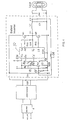
- a self-oscillating driver IC 10 drives half bridge power stages with transistors M1 and M2 generating an AC voltage across the input of a resonant load.
- IC 10 has a built-in oscillator that is, or is similar to, the "555" timer of the prior art.
- Oscillator frequency can be programmed with a timing circuit 12 coupled to pins Rt, Ct and common "com”.
- the feedback circuit includes blocks 14 and 16 that couple inverter high voltage output LH to timing circuit 12.
- Block 14 attenuates the output voltage signal and block 16 phase shifts the output voltage signal from 150° to 200° to compensate for the phase difference between the inverter output voltage and the external synchronization signal.
- Timing circuit 12 may include a timing capacitor Ct and resistor Rt (see Figure 2) and switches when the timing capacitor is charged to 2/3 Vcc and discharged to 1/3 Vcc.
- the timing capacitor voltage waveform is an exponential ramp that is superposed on the DC voltage.
- the IC oscillator correlates its frequency.
- a source of this signal is coupled between ground and the timing capacitor.
- Attenuating block 14 ( Figure 3) includes a capacitive divider with capacitors C4 and C5 connected to inverter high voltage output LH.
- Phase shifting block 16 includes an active signal inverter that includes transistor M3 and resistors R3, R4, R6 and R7. The output of the capacitive divider is connected to the input of the active signal inverter. The output of the active signal inverter is connected to the Ct pin of IC 10 via a second timing capacitor Ct2 and timing circuit 12.
- the active signal inverter provides a stable phase shift of about 180° at any frequency. Thus, the active signal inverter compensates for about 180° of phase difference between the input and output of the open loop inverter operating above resonant frequency.
- the circuit of Figure 4 may include the following components: IC 10 - IR21531D, M3 - BC337, C4 and Ct2 - 22pF, Ct1 - 250pF, C5 - 4.7nF, Rt1 - 10K, R3 - 100k, R7 - 750, R4 - 15k, R6-15k, R15 and R16 - 22k, C26 and C28 - 0.1uF.
- the ballast inverter switches at 250 kHz. With an open loop circuit, the ballast inverter switches at 242 kHz. Resonant frequency of the inverter resonant load is about 220 kHz.
- the sinusoidal signal injected to pin Ct of IC 10 via timing capacitor Ct2 dominates above the ramp signal generated by the timer even though it has a much smaller level than the ramp signal.
- the switching frequency of the inverter depends on the resonant load as in self-generated resonant ballasts without an IC.
- resistive means may be connected between timing capacitor Ct1 and common "com" of IC 10.
- Figure 5 shows two anti-parallel diodes D53 and D55 that may serve as the resistive means, although resistor(s) can be used instead of diodes (for example, see R10 in Figure 6).
- the feedback circuit may include two RC phase-shifting networks that perform the functions of blocks 14 and 16.
- the first network includes a capacitor C6 coupled to high voltage output LH and a resistor R8 coupled to common.
- the second network includes a capacitor C7 and the resistive means.
- the second network is connecter in parallel to resistor R8 of the first network.
- Capacitor C6 may be a high voltage capacitor connected to LH while other components may be low voltage, low power components.
- a phase shift angle of about 150-200 degrees is needed for optimizing the feedback phase lock.
- the two series RC networks provide attenuation of the feedback signal more than 100 times and a programmable phase shifting up to around 180°.
- the ballast inverter starts with a programmed initial switching frequency determined by timing capacitor Ct1 and resistor Rt1. As soon as a voltage appears at LH, the inverter will be internally synchronized as the feedback signal will dominate the "555" timer ramp signal of IC 10. Inverter frequency will be automatically corrected so that input/output phase difference at selected switching frequency will be automatically compensated by the RC phase boosting networks in the feedback circuit.
- FIG. 6 shows a modification of the embodiment of Figure 5 with a third RC phase-shifting network that is added during lamp starting.
- the third RC network includes capacitor C8, resistor R9 and a switching means connected in series with resistor R9.
- the switching means may include two series Zener diodes D3 and D4 connected in opposite directions.
- voltage that is applied across the circuit comprising resistor R9 and Zener diodes D3 and D4 is much higher than the Zener diodes' threshold voltage.
- the peak of this voltage is lower than the Zener diodes' threshold.
- the Zener diodes provide a switching function by adding a third RC phase-shifting network during lamp starting to limit starting voltage. Ballast components should be protected from overstressing in starting and no-load operation modes.
- two anti-parallel diodes (such as in Figure 5) can be used instead resistor R10 for better stability.
- the ballast inverter includes a feedback circuit with a variable structure having three RC phase-shifting networks.
- the first RC-network includes high voltage capacitor C9 and resistor R11.
- the second RC network includes capacitor C10, resistor R12 and Zener diodes D5 and D6.
- the third RC network includes capacitor C11 and anti-parallel diodes D53 and D55 connected between timing capacitor Ct1 and IC 10 common terminal "com”.
- Resistor R13 connected across anti-parallel Zener diodes D5 and D6 is provided when more than 180° phase-shifting is needed in the feedback circuit for optimized steady-state operation of the inverter (for example 200° phase shifting).
- PWM signal controlled switching means for example, transistor M4 in Figure 7
- PWM signal controlled switching means is connected to the Ct pin of IC 10 via resistor R14.
- IC 10 shuts OFF the ballast inverter.
- the ballast inverter turns ON.
- a duty ratio of transistor M4 switching is controlled by a PWM dimmer (not shown in Figure 7).
- resonant frequency of the resonant load is not stable, as it depends on PWM frequency, duty ratio, temperature, etc.
- the internal synchronization circuit shown herein tracks all current variations of the resonant frequency providing operation of the resonant inverter in the safe area above resonant frequency.
- the feedback circuit in Figure 7 was utilized in a 250 kHz ballast with the following components: IC 10 -IR21531D, Rt1-10k, Ct1-270pF, D53 and D55-1N4148, M4-BC337, C9-22pF, R11-1.3k, C10-1nF, R12-1.8k, D5 and D6-16V, 0.5W Zener, and C11-47pF.
- the circuit could provide dimming in the range of 10-100% with up to a 10 kHz PWM signal with high efficiency.
Landscapes
- Circuit Arrangements For Discharge Lamps (AREA)
Applications Claiming Priority (2)
| Application Number | Priority Date | Filing Date | Title |
|---|---|---|---|
| US10/649,898 US6906473B2 (en) | 2003-08-26 | 2003-08-26 | Feedback circuit and method of operating ballast resonant inverter |
| US649898 | 2003-08-26 |
Publications (2)
| Publication Number | Publication Date |
|---|---|
| EP1511364A1 true EP1511364A1 (de) | 2005-03-02 |
| EP1511364B1 EP1511364B1 (de) | 2013-05-08 |
Family
ID=34104689
Family Applications (1)
| Application Number | Title | Priority Date | Filing Date |
|---|---|---|---|
| EP04016556.5A Expired - Lifetime EP1511364B1 (de) | 2003-08-26 | 2004-07-14 | Rückkopplungsschaltung und Verfahren zum Betrieb eines Vorschaltgerät-Resonanzwechselrichters |
Country Status (4)
| Country | Link |
|---|---|
| US (1) | US6906473B2 (de) |
| EP (1) | EP1511364B1 (de) |
| CN (1) | CN1592531B (de) |
| CA (1) | CA2472530C (de) |
Cited By (4)
| Publication number | Priority date | Publication date | Assignee | Title |
|---|---|---|---|---|
| EP2488000A2 (de) * | 2011-02-10 | 2012-08-15 | Osram Sylvania Inc. | Vorschaltgerät mit zwei Beleuchtungsstufen |
| CN104105295A (zh) * | 2013-04-15 | 2014-10-15 | 梅玉刚 | 双全桥注入锁相功率合成金卤灯 |
| CN104105294A (zh) * | 2013-04-15 | 2014-10-15 | 阮树成 | 直流低压电源四推挽注锁功率合成金卤灯 |
| US20220173650A1 (en) * | 2020-11-27 | 2022-06-02 | Fuji Electric Co., Ltd. | Current detection circuit and power supply circuit |
Families Citing this family (30)
| Publication number | Priority date | Publication date | Assignee | Title |
|---|---|---|---|---|
| TWI220853B (en) * | 2003-09-17 | 2004-09-01 | Lite On Technology Corp | Quick warm-up lighting device |
| JP4186801B2 (ja) * | 2003-11-25 | 2008-11-26 | 松下電工株式会社 | 無電極放電灯点灯装置並びに無電極放電灯装置 |
| WO2005072023A1 (en) * | 2004-01-23 | 2005-08-04 | Koninklijke Philips Electronics N.V. | High frequency driver for gas discharge lamp |
| US7471427B2 (en) * | 2004-06-22 | 2008-12-30 | Lite-On Technology Corporation | Warm-up circuit for CCFLs |
| US7619368B2 (en) * | 2005-07-05 | 2009-11-17 | Chao-Cheng Lu | Power source apparatus |
| US7498751B2 (en) * | 2006-06-15 | 2009-03-03 | Himax Technologies Limited | High efficiency and low cost cold cathode fluorescent lamp driving apparatus for LCD backlight |
| TW200812436A (en) * | 2006-08-22 | 2008-03-01 | Beyond Innovation Tech Co Ltd | Electronic ballast and method for driving fluorescent lamp |
| US8018173B2 (en) * | 2006-09-03 | 2011-09-13 | Fulham Company Ltd. | Ballasts for fluorescent lamps |
| US8736189B2 (en) * | 2006-12-23 | 2014-05-27 | Fulham Company Limited | Electronic ballasts with high-frequency-current blocking component or positive current feedback |
| US8058811B2 (en) * | 2007-03-26 | 2011-11-15 | International Rectifier Corporation | HID lamp ballast circuit |
| US20090200952A1 (en) * | 2008-02-08 | 2009-08-13 | Purespectrum, Inc. | Methods and apparatus for dimming light sources |
| US20090200951A1 (en) * | 2008-02-08 | 2009-08-13 | Purespectrum, Inc. | Methods and Apparatus for Dimming Light Sources |
| US20090200964A1 (en) * | 2008-02-08 | 2009-08-13 | King Ray J | Methods And Apparatus For Dimmable Ballasts With A High Power Factor |
| US20090200953A1 (en) * | 2008-02-08 | 2009-08-13 | Ray James King | Methods and apparatus for a high power factor ballast having high efficiency during normal operation and during dimming |
| US20100176733A1 (en) * | 2009-01-14 | 2010-07-15 | Purespectrum, Inc. | Automated Dimming Methods and Systems For Lighting |
| US20100225239A1 (en) * | 2009-03-04 | 2010-09-09 | Purespectrum, Inc. | Methods and apparatus for a high power factor, high efficiency, dimmable, rapid starting cold cathode lighting ballast |
| CN102694473A (zh) * | 2011-03-21 | 2012-09-26 | 国琏电子(上海)有限公司 | 电源供应系统 |
| DE102012101548B4 (de) * | 2012-02-27 | 2015-11-19 | Maschinenfabrik Reinhausen Gmbh | Prüfsystem und Verfahren für eine induzierte Spannungsprüfung sowie Verlustleistungsmessung von Prüfobjekten der Hochspannungstechnik |
| GB2501539B (en) * | 2012-04-27 | 2018-10-24 | Nidec Control Techniques Ltd | Power control system |
| US20140035480A1 (en) * | 2012-08-02 | 2014-02-06 | Tsvi Blumin | Method for the control of luminance of gas discharge lamps |
| CN104105284A (zh) * | 2013-04-15 | 2014-10-15 | 阮雪芬 | 双半桥注入锁相功率合成黑光灯组 |
| CN104105251A (zh) * | 2013-04-15 | 2014-10-15 | 阮树成 | 太阳能电源双全桥注锁发光二极管led阵列灯 |
| CN104105292A (zh) * | 2013-04-15 | 2014-10-15 | 阮树成 | 太阳能电源四全桥注锁功率合成无极灯组 |
| CN103327702B (zh) * | 2013-04-15 | 2015-01-28 | 张根清 | 太阳能电源双半桥注锁功率合成卤素灯组 |
| CN104105316B (zh) * | 2013-04-15 | 2018-01-05 | 张妙娟 | 直流低电压双推注入锁相功率合成低压钠灯 |
| CN104105280B (zh) * | 2013-04-15 | 2018-01-05 | 张妙娟 | 直流低压双推注入锁相功率合成卤钨灯 |
| CN104105325A (zh) * | 2013-04-15 | 2014-10-15 | 张妙娟 | 直流低电压双推注入锁相功率合成无极灯 |
| CN104105319A (zh) * | 2013-04-15 | 2014-10-15 | 阮树成 | 太阳能电源四全桥注锁功率合成荧光灯组 |
| CN104105253B (zh) * | 2013-04-15 | 2017-12-01 | 梅玉刚 | 双全桥注入锁相发光二极管led阵列灯 |
| CN119232026B (zh) * | 2024-12-03 | 2025-04-22 | 凡己科技(苏州)有限公司 | 一种应用于电动大工程机械车辆的电流采样电路及方法 |
Citations (3)
| Publication number | Priority date | Publication date | Assignee | Title |
|---|---|---|---|---|
| US4535399A (en) * | 1983-06-03 | 1985-08-13 | National Semiconductor Corporation | Regulated switched power circuit with resonant load |
| US6016257A (en) * | 1996-12-23 | 2000-01-18 | Philips Electronics North America Corporation | Voltage regulated power supply utilizing phase shift control |
| US6326740B1 (en) * | 1998-12-22 | 2001-12-04 | Philips Electronics North America Corporation | High frequency electronic ballast for multiple lamp independent operation |
Family Cites Families (9)
| Publication number | Priority date | Publication date | Assignee | Title |
|---|---|---|---|---|
| NL8503008A (nl) * | 1985-11-04 | 1987-06-01 | Philips Nv | Gelijkstroom-wisselstroomomzetter voor het ontsteken en voeden van een ontladingslamp. |
| US5245253A (en) | 1989-09-21 | 1993-09-14 | Etta Industries | Electronic dimming methods for solid state electronic ballasts |
| US4998046A (en) | 1989-06-05 | 1991-03-05 | Gte Products Corporation | Synchronized lamp ballast with dimming |
| US5719472A (en) | 1996-05-13 | 1998-02-17 | General Electric Company | High voltage IC-driven half-bridge gas discharge ballast |
| JPH11514146A (ja) * | 1996-08-14 | 1999-11-30 | コーニンクレッカ、フィリップス、エレクトロニクス、エヌ.ヴィ. | 回路装置 |
| US5723953A (en) | 1996-09-19 | 1998-03-03 | General Electric Company | High voltage IC-driven half-bridge gas discharge lamp ballast |
| DE19650110A1 (de) * | 1996-12-03 | 1998-06-04 | Patent Treuhand Ges Fuer Elektrische Gluehlampen Mbh | Betriebsschaltung für eine elektrodenlose Niederdruckentladungslampe |
| US5781418A (en) * | 1996-12-23 | 1998-07-14 | Philips Electronics North America Corporation | Switching scheme for power supply having a voltage-fed inverter |
| US6246183B1 (en) | 2000-02-28 | 2001-06-12 | Litton Systems, Inc. | Dimmable electrodeless light source |
-
2003
- 2003-08-26 US US10/649,898 patent/US6906473B2/en not_active Expired - Lifetime
-
2004
- 2004-06-25 CA CA2472530A patent/CA2472530C/en not_active Expired - Fee Related
- 2004-07-14 EP EP04016556.5A patent/EP1511364B1/de not_active Expired - Lifetime
- 2004-08-26 CN CN2004100685429A patent/CN1592531B/zh not_active Expired - Fee Related
Patent Citations (3)
| Publication number | Priority date | Publication date | Assignee | Title |
|---|---|---|---|---|
| US4535399A (en) * | 1983-06-03 | 1985-08-13 | National Semiconductor Corporation | Regulated switched power circuit with resonant load |
| US6016257A (en) * | 1996-12-23 | 2000-01-18 | Philips Electronics North America Corporation | Voltage regulated power supply utilizing phase shift control |
| US6326740B1 (en) * | 1998-12-22 | 2001-12-04 | Philips Electronics North America Corporation | High frequency electronic ballast for multiple lamp independent operation |
Cited By (5)
| Publication number | Priority date | Publication date | Assignee | Title |
|---|---|---|---|---|
| EP2488000A2 (de) * | 2011-02-10 | 2012-08-15 | Osram Sylvania Inc. | Vorschaltgerät mit zwei Beleuchtungsstufen |
| CN104105295A (zh) * | 2013-04-15 | 2014-10-15 | 梅玉刚 | 双全桥注入锁相功率合成金卤灯 |
| CN104105294A (zh) * | 2013-04-15 | 2014-10-15 | 阮树成 | 直流低压电源四推挽注锁功率合成金卤灯 |
| US20220173650A1 (en) * | 2020-11-27 | 2022-06-02 | Fuji Electric Co., Ltd. | Current detection circuit and power supply circuit |
| US12051964B2 (en) * | 2020-11-27 | 2024-07-30 | Fuji Electric Co., Ltd. | Current detection circuit including non-linear circuit and power supply circuit containing the same |
Also Published As
| Publication number | Publication date |
|---|---|
| EP1511364B1 (de) | 2013-05-08 |
| CA2472530A1 (en) | 2005-02-26 |
| CN1592531B (zh) | 2012-02-08 |
| CN1592531A (zh) | 2005-03-09 |
| US20050046359A1 (en) | 2005-03-03 |
| CA2472530C (en) | 2014-08-05 |
| US6906473B2 (en) | 2005-06-14 |
Similar Documents
| Publication | Publication Date | Title |
|---|---|---|
| EP1511364B1 (de) | Rückkopplungsschaltung und Verfahren zum Betrieb eines Vorschaltgerät-Resonanzwechselrichters | |
| US7911153B2 (en) | Electronic ballasts for lighting systems | |
| US7061188B1 (en) | Instant start electronic ballast with universal AC input voltage | |
| JP3752222B2 (ja) | 高輝度放電ランプ用の調光可能な電子安定器 | |
| KR100858746B1 (ko) | 형광 안정기 제어기 ic | |
| CA2280561C (en) | Electronic high intensity discharge ballast | |
| EP0765108B1 (de) | Anordnung zum Betreiben einer Starkstromentladungslampe | |
| CN100403203C (zh) | 用于调光的冷阴极荧光灯的电子镇流器 | |
| CN102057758A (zh) | 多灯瞬时启动电子镇流器 | |
| WO2002039788A1 (en) | Ballast self oscillating inverter with phase controlled voltage feedback | |
| CA2506406C (en) | Resonant inverter including feed back circuit with source of variable bias current | |
| CA2506402C (en) | Control system for a resonant inverter with self-oscillating driver | |
| Tao et al. | Self-oscillating electronic ballast with dimming control | |
| US6329761B1 (en) | Frequency controlled half-bridge inverter for variable loads | |
| JP2005504427A (ja) | ランプランアップ調整を行う電子的な安定器 | |
| CN101010992A (zh) | 荧光灯镇流器控制器集成电路 | |
| KR200407568Y1 (ko) | 개별디밍에 의한 조광제어부를 갖는 전자식 안정기 | |
| JP2003197394A (ja) | 放電灯点灯装置 |
Legal Events
| Date | Code | Title | Description |
|---|---|---|---|
| PUAI | Public reference made under article 153(3) epc to a published international application that has entered the european phase |
Free format text: ORIGINAL CODE: 0009012 |
|
| AK | Designated contracting states |
Kind code of ref document: A1 Designated state(s): AT BE BG CH CY CZ DE DK EE ES FI FR GB GR HU IE IT LI LU MC NL PL PT RO SE SI SK TR |
|
| AX | Request for extension of the european patent |
Extension state: AL HR LT LV MK |
|
| 17P | Request for examination filed |
Effective date: 20050321 |
|
| AKX | Designation fees paid |
Designated state(s): AT DE FR GB IT SE |
|
| 17Q | First examination report despatched |
Effective date: 20060214 |
|
| GRAP | Despatch of communication of intention to grant a patent |
Free format text: ORIGINAL CODE: EPIDOSNIGR1 |
|
| RIC1 | Information provided on ipc code assigned before grant |
Ipc: H05B 41/285 20060101ALI20121127BHEP Ipc: H05B 41/282 20060101AFI20121127BHEP Ipc: H05B 41/28 20060101ALI20121127BHEP |
|
| GRAS | Grant fee paid |
Free format text: ORIGINAL CODE: EPIDOSNIGR3 |
|
| GRAA | (expected) grant |
Free format text: ORIGINAL CODE: 0009210 |
|
| AK | Designated contracting states |
Kind code of ref document: B1 Designated state(s): AT DE FR GB IT SE |
|
| REG | Reference to a national code |
Ref country code: GB Ref legal event code: FG4D |
|
| REG | Reference to a national code |
Ref country code: AT Ref legal event code: REF Ref document number: 611615 Country of ref document: AT Kind code of ref document: T Effective date: 20130515 |
|
| REG | Reference to a national code |
Ref country code: DE Ref legal event code: R096 Ref document number: 602004042030 Country of ref document: DE Effective date: 20130704 |
|
| REG | Reference to a national code |
Ref country code: SE Ref legal event code: TRGR |
|
| PLBE | No opposition filed within time limit |
Free format text: ORIGINAL CODE: 0009261 |
|
| STAA | Information on the status of an ep patent application or granted ep patent |
Free format text: STATUS: NO OPPOSITION FILED WITHIN TIME LIMIT |
|
| 26N | No opposition filed |
Effective date: 20140211 |
|
| REG | Reference to a national code |
Ref country code: DE Ref legal event code: R097 Ref document number: 602004042030 Country of ref document: DE Effective date: 20140211 |
|
| REG | Reference to a national code |
Ref country code: FR Ref legal event code: PLFP Year of fee payment: 13 |
|
| REG | Reference to a national code |
Ref country code: FR Ref legal event code: PLFP Year of fee payment: 14 |
|
| PGFP | Annual fee paid to national office [announced via postgrant information from national office to epo] |
Ref country code: FR Payment date: 20170724 Year of fee payment: 14 Ref country code: DE Payment date: 20170724 Year of fee payment: 14 Ref country code: GB Payment date: 20170719 Year of fee payment: 14 Ref country code: IT Payment date: 20170728 Year of fee payment: 14 |
|
| PGFP | Annual fee paid to national office [announced via postgrant information from national office to epo] |
Ref country code: SE Payment date: 20170719 Year of fee payment: 14 Ref country code: AT Payment date: 20170720 Year of fee payment: 14 |
|
| REG | Reference to a national code |
Ref country code: DE Ref legal event code: R119 Ref document number: 602004042030 Country of ref document: DE |
|
| REG | Reference to a national code |
Ref country code: AT Ref legal event code: MM01 Ref document number: 611615 Country of ref document: AT Kind code of ref document: T Effective date: 20180714 |
|
| GBPC | Gb: european patent ceased through non-payment of renewal fee |
Effective date: 20180714 |
|
| PG25 | Lapsed in a contracting state [announced via postgrant information from national office to epo] |
Ref country code: FR Free format text: LAPSE BECAUSE OF NON-PAYMENT OF DUE FEES Effective date: 20180731 Ref country code: DE Free format text: LAPSE BECAUSE OF NON-PAYMENT OF DUE FEES Effective date: 20190201 Ref country code: AT Free format text: LAPSE BECAUSE OF NON-PAYMENT OF DUE FEES Effective date: 20180714 Ref country code: GB Free format text: LAPSE BECAUSE OF NON-PAYMENT OF DUE FEES Effective date: 20180714 |
|
| PG25 | Lapsed in a contracting state [announced via postgrant information from national office to epo] |
Ref country code: SE Free format text: LAPSE BECAUSE OF NON-PAYMENT OF DUE FEES Effective date: 20180715 |
|
| PG25 | Lapsed in a contracting state [announced via postgrant information from national office to epo] |
Ref country code: IT Free format text: LAPSE BECAUSE OF NON-PAYMENT OF DUE FEES Effective date: 20180714 |