EP1511175A1 - Vorrichtung und Verfahren zum Erhöhen des Funktionsbereichs einer elektrischen Schaltung - Google Patents
Vorrichtung und Verfahren zum Erhöhen des Funktionsbereichs einer elektrischen Schaltung Download PDFInfo
- Publication number
- EP1511175A1 EP1511175A1 EP04447192A EP04447192A EP1511175A1 EP 1511175 A1 EP1511175 A1 EP 1511175A1 EP 04447192 A EP04447192 A EP 04447192A EP 04447192 A EP04447192 A EP 04447192A EP 1511175 A1 EP1511175 A1 EP 1511175A1
- Authority
- EP
- European Patent Office
- Prior art keywords
- circuit
- voltage
- low
- supply
- signal
- Prior art date
- Legal status (The legal status is an assumption and is not a legal conclusion. Google has not performed a legal analysis and makes no representation as to the accuracy of the status listed.)
- Granted
Links
Images





Classifications
-
- H—ELECTRICITY
- H03—ELECTRONIC CIRCUITRY
- H03L—AUTOMATIC CONTROL, STARTING, SYNCHRONISATION OR STABILISATION OF GENERATORS OF ELECTRONIC OSCILLATIONS OR PULSES
- H03L7/00—Automatic control of frequency or phase; Synchronisation
- H03L7/06—Automatic control of frequency or phase; Synchronisation using a reference signal applied to a frequency- or phase-locked loop
- H03L7/08—Details of the phase-locked loop
- H03L7/085—Details of the phase-locked loop concerning mainly the frequency- or phase-detection arrangement including the filtering or amplification of its output signal
- H03L7/089—Details of the phase-locked loop concerning mainly the frequency- or phase-detection arrangement including the filtering or amplification of its output signal the phase or frequency detector generating up-down pulses
- H03L7/0891—Details of the phase-locked loop concerning mainly the frequency- or phase-detection arrangement including the filtering or amplification of its output signal the phase or frequency detector generating up-down pulses the up-down pulses controlling source and sink current generators, e.g. a charge pump
- H03L7/0895—Details of the current generators
-
- H—ELECTRICITY
- H03—ELECTRONIC CIRCUITRY
- H03L—AUTOMATIC CONTROL, STARTING, SYNCHRONISATION OR STABILISATION OF GENERATORS OF ELECTRONIC OSCILLATIONS OR PULSES
- H03L7/00—Automatic control of frequency or phase; Synchronisation
- H03L7/06—Automatic control of frequency or phase; Synchronisation using a reference signal applied to a frequency- or phase-locked loop
- H03L7/08—Details of the phase-locked loop
- H03L7/085—Details of the phase-locked loop concerning mainly the frequency- or phase-detection arrangement including the filtering or amplification of its output signal
- H03L7/089—Details of the phase-locked loop concerning mainly the frequency- or phase-detection arrangement including the filtering or amplification of its output signal the phase or frequency detector generating up-down pulses
- H03L7/0891—Details of the phase-locked loop concerning mainly the frequency- or phase-detection arrangement including the filtering or amplification of its output signal the phase or frequency detector generating up-down pulses the up-down pulses controlling source and sink current generators, e.g. a charge pump
- H03L7/0895—Details of the current generators
- H03L7/0896—Details of the current generators the current generators being controlled by differential up-down pulses
Definitions
- the present invention is related to a device and method for increasing the operating range of an electrical circuit.
- Tunable Micro Electro-Mechanical Systems (MEMS) components appear more and more in RF circuits of wireless communication systems. They allow for new functionality or for improved performance of e.g. electrostatically tuned variable capacitors. In this way the linearity of tunable RF filters can be improved or the phase noise behaviour of voltage-controlled oscillators can be enhanced.
- the tuning voltage required by such devices is typically between 5V and 50V, which is much higher than the maximum supply voltage of a sub-micron CMOS technology. Although the required tuning voltage of these devices can be changed by design, it is unlikely to go below the rapidly decreasing supply voltage of scaled CMOS technologies.
- a PLL circuit which uses a DC-DC converter to set the entire supply voltage to a low value without raising the control voltage sensitivity of a VCO.
- Said DC-DC converter generates a supply voltage to a charge pump and can be switched to operation when the circuit is in the non-locked state and to stop when it is in the locked state.
- the present invention aims to provide a device and method for increasing the operating range of an electrical circuit overcoming the difficulties encountered in the state of the art.
- the present invention relates to a circuit for delivering current at a voltage higher than its supply voltage comprising a first circuit, a second circuit and a high voltage generator.
- the first circuit is arranged for receiving at least one low voltage signal at its input and providing an output voltage signal
- the second circuit is arranged for receiving a clock signal and said output voltage signal.
- the second circuit further comprises means to send a request signal to the high voltage generator, which is adapted for sending two supply voltage signals to the first and the second circuit.
- the two supply voltage signals have a constant voltage difference.
- the high voltage generator comprises means for adjusting the two supply voltage signals such that the voltage of the output voltage signal falls between two reference voltage signals derived from the supply voltages.
- the first and the second circuit are both in a high voltage power region and the high voltage generator in a low voltage power region.
- a level converter is used to provide the transition between the high and the low voltage power supply region.
- the level converter can be implemented as a coupling capacitor.
- the second circuit advantageously comprises a comparator, comparing a voltage signal derived from said output voltage signal with a reference voltage signal derived from the supply voltages.
- the comparator can be implemented as a sense amplifier latch.
- the second circuit may further comprise an operational transconductance amplifier.
- the first circuit comprises a charge pump for a phase-locked loop.
- the first circuit comprises an operational amplifier.
- the high voltage generator preferably comprises a number of identical stages, the last of said stages being permanently clocked.
- Each of said stages consists of two cells connected in parallel, one cell being adapted to pump charge up and one being adapted to pump charge down.
- a circuit as described above is advantageously comprised in a Phase-Locked Loop with a MEMS variable capacitor or in a MEMS switch.
- the invention relates to a method for increasing the operating range of an electrical circuit, comprising the steps of
- the first and the second circuit are both in a high voltage power region and the high voltage generator in a low voltage power region.
- a level converter is used for the transitions between said high and said low voltage power supply region in the described method.
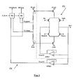
- Fig. 1 represents a general scheme, comprising a first circuit C1 and a second circuit C2 in a high-voltage supply region and a high voltage generator HVG in a low voltage supply region.
- Fig. 2 represents the high supply voltage region containing the core charge pump and two sense amplifier latches.
- Fig. 3 represents high voltage generator (HVG) consisting of 10 identical stages + 1 other stage.
- Fig. 4 shows every stage of the high voltage generator consists of a cell that can pump charge up (top) and a cell that can pump charge down (bottom).
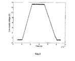
- Fig. 5 represents the transient measurement of the low supply rail of the high voltage region.
- Fig. 6 represents the measured current through an N-well to substrate junction as a function of the bias voltage for 0.18 ⁇ m CMOS.
- Fig. 7 represents some simulation results.
- Fig. 8 represents an embodiment of the invention as a current source.
- the invention discloses a control circuit for a MEMS variable capacitor that dynamically adjusts the power supply while putting only a limited voltage over the output stage of the high voltage control circuit. It does not require any dedicated technology or devices except for a triple well, which is quite standard in nowadays CMOS processes with analogue options.
- the output voltage is in this case only limited by the N-well to substrate breakdown voltage.
- This system realises a 'power supply on demand'. It is applied to a high-voltage charge pump for use in a phase-locked loop (PLL) with a MEMS variable capacitor. Throughout this description 'charge pump' will be used in this meaning, i.e. as used in a phase-locked loop.
- Figure 1 represents a general scheme of the control circuit. It comprises a first circuit (C1) and a second circuit (C2) both in a high voltage power supply region, and a high voltage generator (HVG) in a low voltage power supply region.
- the first circuit (C1) receives at its input low voltage signals (Up and Down) that have been converted to the high voltage power supply region and provides an output voltage signal (Out).
- the second circuit (C2) receives a (converted) clock signal Clk and said output voltage signal (Out). It further comprises means to send a request signal (HVGdown, HVGup) to the high voltage generator, that sends two supply voltage signals (High and Low) to C1 and C2.
- a high voltage charge pump (HVCP) designed for use as charge pump of a PLL has the same connections (up and down signals) as a standard charge pump. So to the system designer it acts as a standard one. It has however a large output voltage range, which is obtained by extending a standard charge pump with said power supply on demand.
- the HVCP consists of two major parts: the core charge pump with sense amplifier latches in the high power supply region and the high-voltage generator (HVG) in the low supply region, with an external ground and 1.8V supply. Signals go from one region to another through a level converter (LC).
- the level converter can further comprise means for buffering the signals.
- the level converter can be a coupling capacitor. So, the two parts are in separate power supply regions and together they form a closed control loop. The goal of this loop is to keep the output voltage of the core charge pump in the middle between the high and the low power supply rail ('high' and 'low'). Both supply rails of the core charge pump region are adjusted, but their voltage difference is constant. This makes the charge pump very linear over a large voltage range, as the voltage over the output transistors is constant.
- the output voltage of the charge pump (Fig. 2) is the reference to which the other voltages of the system are adjusted. It is buffered with two symmetrical operational transconductance amplifiers (OTA1 and OTA2) and then compared to two reference voltages (V upper and V lower ) with sense amplifier (SA) latches.
- the references are e.g. at 40% and 60% between the high and the low supply rail of the core charge pump. An output voltage outside this range results in a request signal (HVGup, HVGdown) to adjust the supply. For example, if the output decreases below the lower reference voltage, the supply voltages of the core charge pump ('High', 'Low') are decreased until the lower limit drops below the output again.
- the supply voltage of the core charge pump is provided by the high voltage generator (HVG) (Fig. 3).
- the HVG consists of a number of identical stages that can pump charge either up or down. The last stage is permanently clocked to generate the supply of the high voltage region. The number of stages is determined by the required output voltage range and is limited by the characteristic of the N-well to substrate junction, which depends on the applied technology (cfr. infra). So, the HVG can generate voltages much higher than its own supply voltage (typically 1.8V for 0.18 ⁇ m CMOS).
- Every stage (Fig. 4) of the HVG consists of two basic cells connected in parallel: one to pump charge up and one to pump charge down. Each stage is located in a separate N-well, which is charged to its own output voltage.
- the basic cell of the HVG consists of two capacitors and two inverters.
- the inverters are realised with standard low voltage transistors as none of the voltages over these transistors exceeds the supply voltage.
- the HVG is driven by two complementary clock signals. This simple two-phase clocking scheme allows a high clock frequency (> 50 MHz). All stages of the HVG except the last are conditionally clocked.
- the HVGup and HVGdown signals are the request signals coming from the core charge pump. The last stage is continuously clocked to generate the power supply of the high-voltage region.
- the capacitance C is the coupling capacitance in the control lines (HVGup, HVGupb) and C par is parasitic capacitance at the internal nodes of the basic cell, not at the input and output nodes.
- the presence of the DOWN cell does not limit the voltage gain of the UP cell.
- the transistors of the UP cell themselves form a large part of the parasitic capacitance. This implies these transistors should be small.
- V dd denotes the supply voltage, e.g.
- the second term depends on the output current, so one has to differentiate between the final stage that generates the supply in high supply region and the intermediate stages that change the absolute voltage of that region.
- R switch denotes the resistance of the transistors when conducting.
- the final stage permanently supplies a current to the circuits in the high supply region, so R out has to be small enough to limit the voltage loss in this stage. This implies transistors with a small on-resistance and a large capacitor and/or high clock frequency. For the other stages the situation is different. If this charge pump is used to control an electrostatically tuned varicap then only the (dis)charge current of the varicap and the high supply region has to be delivered. There is no static current flowing, meaning that the maximum voltage is defined only by the capacitance ratio.
- the high voltage charge pump is processed in a 0.18 ⁇ m CMOS technology. It has a pad-limited die size of 700 ⁇ m*700 ⁇ m, but the circuit area is only 300 ⁇ m*430 ⁇ m.
- the proposed circuit will now be shown to have a very large output voltage range and to be a low power solution scalable to future CMOS generations.
- the high voltage charge pump is measured with a load capacitance C load of 22pF at the output and the oscilloscope connected to the low supply rail of the high voltage region.
- the input resistance of the oscilloscope is 1 M ⁇ , which is too low to connect directly to the charge pump output.
- Supply 1.8 V Number of stages 10+1 Load 22 pF Clock frequency 50 MHz Up and Down signals Frequency 100 kHz Duty cycle 20%
- the up and down pulses are very small so that the current consumption will be very close to this 85 ⁇ A, so this can be regarded as a low power solution.
- the clock is also turned off, the supply current drops to only a few nA.
- the high voltage generator has 10+1 stages and a supply of 1.8V, so the theoretical maximum output voltage (without parasitic capacitances) is 19.8V. However, the measurement shows only 13.2V at the 'Low' node plus 1.6V over the final stage, which is only 14.8V. This difference is larger than what is expected based on the parasitic capacitance, but it is explained by the characteristics of the N-well to substrate junction.
- the high supply voltage region is inside an N-well, which is charged to the high supply rail of this region.
- the highest possible voltage in the system is the breakdown voltage of the well to substrate junction, which is 14.8V for the used technology (Fig. 6). Any attempt to charge the well to a higher voltage results in charge flowing away to the substrate.
- the invention discloses a current source able to deliver current at a voltage higher than its supply voltage.
- the voltage sources in fact represent the high voltage generator.
- the voltage source at the top corresponds to the last cell shown in Fig. 3.
- the voltage source at the bottom corresponds to the 10 identical HVG cells of Fig.3.
- Circuit C1 (as in Fig.2) is represented by the two current sources.
- the bottom voltage source is regulated such that the output voltage is between the voltages on the two sides of the top voltage source.
- the feedback circuit that performs this regulation is not shown in Fig.8.
Landscapes
- Dc-Dc Converters (AREA)
Priority Applications (1)
| Application Number | Priority Date | Filing Date | Title |
|---|---|---|---|
| EP20040447192 EP1511175B1 (de) | 2003-08-28 | 2004-08-25 | Vorrichtung und Verfahren zum Erhöhen des Funktionsbereichs einer elektrischen Schaltung |
Applications Claiming Priority (5)
| Application Number | Priority Date | Filing Date | Title |
|---|---|---|---|
| US499286 | 1983-05-31 | ||
| US49928603P | 2003-08-28 | 2003-08-28 | |
| EP03447224 | 2003-09-08 | ||
| EP03447224 | 2003-09-08 | ||
| EP20040447192 EP1511175B1 (de) | 2003-08-28 | 2004-08-25 | Vorrichtung und Verfahren zum Erhöhen des Funktionsbereichs einer elektrischen Schaltung |
Publications (2)
| Publication Number | Publication Date |
|---|---|
| EP1511175A1 true EP1511175A1 (de) | 2005-03-02 |
| EP1511175B1 EP1511175B1 (de) | 2007-03-28 |
Family
ID=34381605
Family Applications (1)
| Application Number | Title | Priority Date | Filing Date |
|---|---|---|---|
| EP20040447192 Expired - Lifetime EP1511175B1 (de) | 2003-08-28 | 2004-08-25 | Vorrichtung und Verfahren zum Erhöhen des Funktionsbereichs einer elektrischen Schaltung |
Country Status (1)
| Country | Link |
|---|---|
| EP (1) | EP1511175B1 (de) |
Citations (4)
| Publication number | Priority date | Publication date | Assignee | Title |
|---|---|---|---|---|
| JPH10256903A (ja) * | 1997-03-07 | 1998-09-25 | Murata Mfg Co Ltd | Pll回路 |
| US6094102A (en) * | 1999-04-30 | 2000-07-25 | Rockwell Science Center, Llc | Frequency synthesizer using micro electro mechanical systems (MEMS) technology and method |
| US6157821A (en) * | 1997-10-23 | 2000-12-05 | Ericsson Inc. | Voltage step up for a low voltage frequency synthesizer architecture |
| WO2004042926A1 (en) * | 2002-10-30 | 2004-05-21 | Freescale Semiconductor, Inc. | Capacitive charge pump |
-
2004
- 2004-08-25 EP EP20040447192 patent/EP1511175B1/de not_active Expired - Lifetime
Patent Citations (4)
| Publication number | Priority date | Publication date | Assignee | Title |
|---|---|---|---|---|
| JPH10256903A (ja) * | 1997-03-07 | 1998-09-25 | Murata Mfg Co Ltd | Pll回路 |
| US6157821A (en) * | 1997-10-23 | 2000-12-05 | Ericsson Inc. | Voltage step up for a low voltage frequency synthesizer architecture |
| US6094102A (en) * | 1999-04-30 | 2000-07-25 | Rockwell Science Center, Llc | Frequency synthesizer using micro electro mechanical systems (MEMS) technology and method |
| WO2004042926A1 (en) * | 2002-10-30 | 2004-05-21 | Freescale Semiconductor, Inc. | Capacitive charge pump |
Non-Patent Citations (3)
| Title |
|---|
| FAVRAT P ET AL: "A 1.5-V-SUPPLIED CMOS ASIC FOR THE ACTUATION OF AN ELECTROSTATIC MICROMOTOR", IEEE / ASME TRANSACTIONS ON MECHATRONICS, IEEE SERVICE CENTER, PISCATAWAY, NJ, US, vol. 2, no. 3, 1 September 1997 (1997-09-01), pages 153 - 160, XP000724256, ISSN: 1083-4435 * |
| PATENT ABSTRACTS OF JAPAN vol. 1998, no. 14 31 December 1998 (1998-12-31) * |
| R. NADAL-GUARDIA ET AL.: "Current Drive Methods to Extend the Range of Travel of Electrostatic Microactuators Beyond the Voltage Pull-In Point", JOURNAL OF MICROELECTROMECHANICAL SYSTEMS, vol. 11, no. 3, June 2002 (2002-06-01), pages 255 - 263, XP002274234 * |
Also Published As
| Publication number | Publication date |
|---|---|
| EP1511175B1 (de) | 2007-03-28 |
Similar Documents
| Publication | Publication Date | Title |
|---|---|---|
| US10965276B2 (en) | Low noise charge pump method and apparatus | |
| US6859091B1 (en) | Continuous linear regulated zero dropout charge pump with high efficiency load predictive clocking scheme | |
| US6414863B1 (en) | Frequency control circuit for unregulated inductorless DC/DC converters | |
| JP6118809B2 (ja) | マスタースレーブ低ノイズチャージポンプ回路及び方法 | |
| US6320435B1 (en) | PLL circuit which can reduce phase offset without increase in operation voltage | |
| Li et al. | A 90–240 MHz hysteretic controlled DC-DC buck converter with digital phase locked loop synchronization | |
| US8503203B1 (en) | Pre-charge of switched capacitor circuits with cascoded drivers | |
| US6011440A (en) | Amplifier having output range that exceeds supply voltage | |
| US8525564B2 (en) | Charge-based phase locked loop charge pump | |
| US8188777B2 (en) | Charge pump circuit and PLL circuit using the same | |
| KR101805138B1 (ko) | 차지-리사이클링 회로들 | |
| US6972973B2 (en) | Voltage booster having noise reducing structure | |
| US7176732B2 (en) | Device and method for increasing the operating range of an electrical circuit | |
| Innocent et al. | A linear high voltage charge pump for MEMs applications in 0.18/spl mu/m CMOS technology | |
| EP0945986A2 (de) | Ladungspumpenschaltung für eine Phasenregelschleife | |
| EP3248388B1 (de) | Impedanzschaltkreis für ladungspumpenanordnung und ladungspumpenanordnung | |
| US20100301951A1 (en) | Current controlled ring oscillator and method for controlling the same | |
| TW504904B (en) | Voltage controlled oscillator and PLL circuit using the voltage controlled oscillator | |
| EP1511175B1 (de) | Vorrichtung und Verfahren zum Erhöhen des Funktionsbereichs einer elektrischen Schaltung | |
| Alameh et al. | A wide voltage range charge pump in 0.13 μm CMOS for biasing of MEMS resonators | |
| CN117811362B (zh) | 电荷泵电路 | |
| US6590459B2 (en) | Phase lock circuit | |
| CN100385790C (zh) | 可减低时钟馈通效应的切换式电容电路与相关方法 | |
| JP2007202057A (ja) | チャージポンプ回路 | |
| Miresan et al. | Research Article Multipurpose Drivers for MEMS Devices Based on a Single ASIC Implemented in a Low-Cost HV CMOS Process without a Triple Well |
Legal Events
| Date | Code | Title | Description |
|---|---|---|---|
| PUAI | Public reference made under article 153(3) epc to a published international application that has entered the european phase |
Free format text: ORIGINAL CODE: 0009012 |
|
| AK | Designated contracting states |
Kind code of ref document: A1 Designated state(s): AT BE BG CH CY CZ DE DK EE ES FI FR GB GR HU IE IT LI LU MC NL PL PT RO SE SI SK TR |
|
| AX | Request for extension of the european patent |
Extension state: AL HR LT LV MK |
|
| 17P | Request for examination filed |
Effective date: 20050413 |
|
| GRAP | Despatch of communication of intention to grant a patent |
Free format text: ORIGINAL CODE: EPIDOSNIGR1 |
|
| GRAS | Grant fee paid |
Free format text: ORIGINAL CODE: EPIDOSNIGR3 |
|
| AKX | Designation fees paid |
Designated state(s): AT BE BG CH CY CZ DE DK EE ES FI FR GB GR HU IE IT LI LU MC NL PL PT RO SE SI SK TR |
|
| GRAA | (expected) grant |
Free format text: ORIGINAL CODE: 0009210 |
|
| AK | Designated contracting states |
Kind code of ref document: B1 Designated state(s): AT BE BG CH CY CZ DE DK EE ES FI FR GB GR HU IE IT LI LU MC NL PL PT RO SE SI SK TR |
|
| PG25 | Lapsed in a contracting state [announced via postgrant information from national office to epo] |
Ref country code: SI Free format text: LAPSE BECAUSE OF FAILURE TO SUBMIT A TRANSLATION OF THE DESCRIPTION OR TO PAY THE FEE WITHIN THE PRESCRIBED TIME-LIMIT Effective date: 20070328 Ref country code: PL Free format text: LAPSE BECAUSE OF FAILURE TO SUBMIT A TRANSLATION OF THE DESCRIPTION OR TO PAY THE FEE WITHIN THE PRESCRIBED TIME-LIMIT Effective date: 20070328 Ref country code: AT Free format text: LAPSE BECAUSE OF FAILURE TO SUBMIT A TRANSLATION OF THE DESCRIPTION OR TO PAY THE FEE WITHIN THE PRESCRIBED TIME-LIMIT Effective date: 20070328 Ref country code: NL Free format text: LAPSE BECAUSE OF FAILURE TO SUBMIT A TRANSLATION OF THE DESCRIPTION OR TO PAY THE FEE WITHIN THE PRESCRIBED TIME-LIMIT Effective date: 20070328 Ref country code: LI Free format text: LAPSE BECAUSE OF FAILURE TO SUBMIT A TRANSLATION OF THE DESCRIPTION OR TO PAY THE FEE WITHIN THE PRESCRIBED TIME-LIMIT Effective date: 20070328 Ref country code: FI Free format text: LAPSE BECAUSE OF FAILURE TO SUBMIT A TRANSLATION OF THE DESCRIPTION OR TO PAY THE FEE WITHIN THE PRESCRIBED TIME-LIMIT Effective date: 20070328 Ref country code: BE Free format text: LAPSE BECAUSE OF FAILURE TO SUBMIT A TRANSLATION OF THE DESCRIPTION OR TO PAY THE FEE WITHIN THE PRESCRIBED TIME-LIMIT Effective date: 20070328 Ref country code: CH Free format text: LAPSE BECAUSE OF FAILURE TO SUBMIT A TRANSLATION OF THE DESCRIPTION OR TO PAY THE FEE WITHIN THE PRESCRIBED TIME-LIMIT Effective date: 20070328 |
|
| REG | Reference to a national code |
Ref country code: GB Ref legal event code: FG4D |
|
| REG | Reference to a national code |
Ref country code: CH Ref legal event code: EP |
|
| REF | Corresponds to: |
Ref document number: 602004005543 Country of ref document: DE Date of ref document: 20070510 Kind code of ref document: P |
|
| REG | Reference to a national code |
Ref country code: IE Ref legal event code: FG4D |
|
| PG25 | Lapsed in a contracting state [announced via postgrant information from national office to epo] |
Ref country code: SE Free format text: LAPSE BECAUSE OF FAILURE TO SUBMIT A TRANSLATION OF THE DESCRIPTION OR TO PAY THE FEE WITHIN THE PRESCRIBED TIME-LIMIT Effective date: 20070628 |
|
| PG25 | Lapsed in a contracting state [announced via postgrant information from national office to epo] |
Ref country code: ES Free format text: LAPSE BECAUSE OF FAILURE TO SUBMIT A TRANSLATION OF THE DESCRIPTION OR TO PAY THE FEE WITHIN THE PRESCRIBED TIME-LIMIT Effective date: 20070709 |
|
| PG25 | Lapsed in a contracting state [announced via postgrant information from national office to epo] |
Ref country code: PT Free format text: LAPSE BECAUSE OF FAILURE TO SUBMIT A TRANSLATION OF THE DESCRIPTION OR TO PAY THE FEE WITHIN THE PRESCRIBED TIME-LIMIT Effective date: 20070828 |
|
| REG | Reference to a national code |
Ref country code: CH Ref legal event code: PL |
|
| NLV1 | Nl: lapsed or annulled due to failure to fulfill the requirements of art. 29p and 29m of the patents act | ||
| ET | Fr: translation filed | ||
| PG25 | Lapsed in a contracting state [announced via postgrant information from national office to epo] |
Ref country code: SK Free format text: LAPSE BECAUSE OF FAILURE TO SUBMIT A TRANSLATION OF THE DESCRIPTION OR TO PAY THE FEE WITHIN THE PRESCRIBED TIME-LIMIT Effective date: 20070328 |
|
| PG25 | Lapsed in a contracting state [announced via postgrant information from national office to epo] |
Ref country code: RO Free format text: LAPSE BECAUSE OF FAILURE TO SUBMIT A TRANSLATION OF THE DESCRIPTION OR TO PAY THE FEE WITHIN THE PRESCRIBED TIME-LIMIT Effective date: 20070328 Ref country code: CZ Free format text: LAPSE BECAUSE OF FAILURE TO SUBMIT A TRANSLATION OF THE DESCRIPTION OR TO PAY THE FEE WITHIN THE PRESCRIBED TIME-LIMIT Effective date: 20070328 |
|
| PG25 | Lapsed in a contracting state [announced via postgrant information from national office to epo] |
Ref country code: DK Free format text: LAPSE BECAUSE OF FAILURE TO SUBMIT A TRANSLATION OF THE DESCRIPTION OR TO PAY THE FEE WITHIN THE PRESCRIBED TIME-LIMIT Effective date: 20070328 |
|
| PLBE | No opposition filed within time limit |
Free format text: ORIGINAL CODE: 0009261 |
|
| STAA | Information on the status of an ep patent application or granted ep patent |
Free format text: STATUS: NO OPPOSITION FILED WITHIN TIME LIMIT |
|
| 26N | No opposition filed |
Effective date: 20080102 |
|
| PG25 | Lapsed in a contracting state [announced via postgrant information from national office to epo] |
Ref country code: IT Free format text: LAPSE BECAUSE OF FAILURE TO SUBMIT A TRANSLATION OF THE DESCRIPTION OR TO PAY THE FEE WITHIN THE PRESCRIBED TIME-LIMIT Effective date: 20070328 Ref country code: MC Free format text: LAPSE BECAUSE OF NON-PAYMENT OF DUE FEES Effective date: 20070831 Ref country code: GR Free format text: LAPSE BECAUSE OF FAILURE TO SUBMIT A TRANSLATION OF THE DESCRIPTION OR TO PAY THE FEE WITHIN THE PRESCRIBED TIME-LIMIT Effective date: 20070629 |
|
| PG25 | Lapsed in a contracting state [announced via postgrant information from national office to epo] |
Ref country code: IE Free format text: LAPSE BECAUSE OF NON-PAYMENT OF DUE FEES Effective date: 20070827 |
|
| PG25 | Lapsed in a contracting state [announced via postgrant information from national office to epo] |
Ref country code: EE Free format text: LAPSE BECAUSE OF FAILURE TO SUBMIT A TRANSLATION OF THE DESCRIPTION OR TO PAY THE FEE WITHIN THE PRESCRIBED TIME-LIMIT Effective date: 20070328 |
|
| PG25 | Lapsed in a contracting state [announced via postgrant information from national office to epo] |
Ref country code: CY Free format text: LAPSE BECAUSE OF FAILURE TO SUBMIT A TRANSLATION OF THE DESCRIPTION OR TO PAY THE FEE WITHIN THE PRESCRIBED TIME-LIMIT Effective date: 20070328 |
|
| PG25 | Lapsed in a contracting state [announced via postgrant information from national office to epo] |
Ref country code: LU Free format text: LAPSE BECAUSE OF NON-PAYMENT OF DUE FEES Effective date: 20070825 Ref country code: BG Free format text: LAPSE BECAUSE OF FAILURE TO SUBMIT A TRANSLATION OF THE DESCRIPTION OR TO PAY THE FEE WITHIN THE PRESCRIBED TIME-LIMIT Effective date: 20070628 |
|
| PG25 | Lapsed in a contracting state [announced via postgrant information from national office to epo] |
Ref country code: HU Free format text: LAPSE BECAUSE OF FAILURE TO SUBMIT A TRANSLATION OF THE DESCRIPTION OR TO PAY THE FEE WITHIN THE PRESCRIBED TIME-LIMIT Effective date: 20070929 Ref country code: TR Free format text: LAPSE BECAUSE OF FAILURE TO SUBMIT A TRANSLATION OF THE DESCRIPTION OR TO PAY THE FEE WITHIN THE PRESCRIBED TIME-LIMIT Effective date: 20070328 |
|
| PGFP | Annual fee paid to national office [announced via postgrant information from national office to epo] |
Ref country code: GB Payment date: 20120725 Year of fee payment: 9 |
|
| PGFP | Annual fee paid to national office [announced via postgrant information from national office to epo] |
Ref country code: FR Payment date: 20120906 Year of fee payment: 9 Ref country code: DE Payment date: 20120723 Year of fee payment: 9 |
|
| GBPC | Gb: european patent ceased through non-payment of renewal fee |
Effective date: 20130825 |
|
| PG25 | Lapsed in a contracting state [announced via postgrant information from national office to epo] |
Ref country code: DE Free format text: LAPSE BECAUSE OF NON-PAYMENT OF DUE FEES Effective date: 20140301 |
|
| REG | Reference to a national code |
Ref country code: DE Ref legal event code: R119 Ref document number: 602004005543 Country of ref document: DE Effective date: 20140301 |
|
| REG | Reference to a national code |
Ref country code: FR Ref legal event code: ST Effective date: 20140430 |
|
| PG25 | Lapsed in a contracting state [announced via postgrant information from national office to epo] |
Ref country code: GB Free format text: LAPSE BECAUSE OF NON-PAYMENT OF DUE FEES Effective date: 20130825 |
|
| PG25 | Lapsed in a contracting state [announced via postgrant information from national office to epo] |
Ref country code: FR Free format text: LAPSE BECAUSE OF NON-PAYMENT OF DUE FEES Effective date: 20130902 |