EP1508908A2 - Contacts électriques, appareil électrique et procédé pour la détection d'usure des contacts électriques - Google Patents
Contacts électriques, appareil électrique et procédé pour la détection d'usure des contacts électriques Download PDFInfo
- Publication number
- EP1508908A2 EP1508908A2 EP04019801A EP04019801A EP1508908A2 EP 1508908 A2 EP1508908 A2 EP 1508908A2 EP 04019801 A EP04019801 A EP 04019801A EP 04019801 A EP04019801 A EP 04019801A EP 1508908 A2 EP1508908 A2 EP 1508908A2
- Authority
- EP
- European Patent Office
- Prior art keywords
- electric contacts
- light
- electric
- opening
- abrasion
- Prior art date
- Legal status (The legal status is an assumption and is not a legal conclusion. Google has not performed a legal analysis and makes no representation as to the accuracy of the status listed.)
- Granted
Links
- 238000005299 abrasion Methods 0.000 title claims abstract description 80
- 238000000034 method Methods 0.000 title claims description 21
- 238000001514 detection method Methods 0.000 claims abstract description 32
- 238000012545 processing Methods 0.000 claims description 72
- 239000000463 material Substances 0.000 claims description 53
- 239000013307 optical fiber Substances 0.000 claims description 33
- 230000002093 peripheral effect Effects 0.000 claims description 14
- 229910052738 indium Inorganic materials 0.000 claims description 9
- 229910052751 metal Inorganic materials 0.000 claims description 9
- 239000002184 metal Substances 0.000 claims description 9
- 229910052804 chromium Inorganic materials 0.000 claims description 6
- 239000000956 alloy Substances 0.000 claims description 5
- 229910045601 alloy Inorganic materials 0.000 claims description 5
- 230000005540 biological transmission Effects 0.000 claims description 4
- 238000000354 decomposition reaction Methods 0.000 claims description 3
- 229910052797 bismuth Inorganic materials 0.000 claims 1
- 229910052758 niobium Inorganic materials 0.000 claims 1
- 229910052702 rhenium Inorganic materials 0.000 claims 1
- 229910052712 strontium Inorganic materials 0.000 claims 1
- 239000010410 layer Substances 0.000 description 125
- 238000000295 emission spectrum Methods 0.000 description 11
- 239000010949 copper Substances 0.000 description 9
- 229910052782 aluminium Inorganic materials 0.000 description 7
- XAGFODPZIPBFFR-UHFFFAOYSA-N aluminium Chemical compound [Al] XAGFODPZIPBFFR-UHFFFAOYSA-N 0.000 description 7
- APFVFJFRJDLVQX-UHFFFAOYSA-N indium atom Chemical compound [In] APFVFJFRJDLVQX-UHFFFAOYSA-N 0.000 description 7
- 238000007747 plating Methods 0.000 description 7
- 238000003466 welding Methods 0.000 description 7
- VYZAMTAEIAYCRO-UHFFFAOYSA-N Chromium Chemical compound [Cr] VYZAMTAEIAYCRO-UHFFFAOYSA-N 0.000 description 6
- RYGMFSIKBFXOCR-UHFFFAOYSA-N Copper Chemical compound [Cu] RYGMFSIKBFXOCR-UHFFFAOYSA-N 0.000 description 6
- BQCADISMDOOEFD-UHFFFAOYSA-N Silver Chemical compound [Ag] BQCADISMDOOEFD-UHFFFAOYSA-N 0.000 description 6
- 230000005856 abnormality Effects 0.000 description 6
- 229910052802 copper Inorganic materials 0.000 description 6
- 229910052709 silver Inorganic materials 0.000 description 6
- 239000004332 silver Substances 0.000 description 6
- 239000011651 chromium Substances 0.000 description 5
- 238000005259 measurement Methods 0.000 description 5
- 238000012986 modification Methods 0.000 description 5
- 230000004048 modification Effects 0.000 description 5
- 239000004020 conductor Substances 0.000 description 3
- 238000001513 hot isostatic pressing Methods 0.000 description 3
- 238000007751 thermal spraying Methods 0.000 description 3
- 230000002159 abnormal effect Effects 0.000 description 2
- 230000015572 biosynthetic process Effects 0.000 description 2
- 238000005253 cladding Methods 0.000 description 2
- 238000007598 dipping method Methods 0.000 description 2
- 238000007772 electroless plating Methods 0.000 description 2
- 238000009713 electroplating Methods 0.000 description 2
- 238000004519 manufacturing process Methods 0.000 description 2
- ATJFFYVFTNAWJD-UHFFFAOYSA-N Tin Chemical compound [Sn] ATJFFYVFTNAWJD-UHFFFAOYSA-N 0.000 description 1
- 238000010521 absorption reaction Methods 0.000 description 1
- 230000001133 acceleration Effects 0.000 description 1
- 230000006978 adaptation Effects 0.000 description 1
- 230000000903 blocking effect Effects 0.000 description 1
- 230000000694 effects Effects 0.000 description 1
- 238000010438 heat treatment Methods 0.000 description 1
- 238000003754 machining Methods 0.000 description 1
- 238000012423 maintenance Methods 0.000 description 1
- 150000002739 metals Chemical class 0.000 description 1
- 239000000203 mixture Substances 0.000 description 1
- 238000012544 monitoring process Methods 0.000 description 1
- 230000003287 optical effect Effects 0.000 description 1
- 230000035945 sensitivity Effects 0.000 description 1
- 238000001179 sorption measurement Methods 0.000 description 1
- 238000001228 spectrum Methods 0.000 description 1
- 239000002344 surface layer Substances 0.000 description 1
- JBQYATWDVHIOAR-UHFFFAOYSA-N tellanylidenegermanium Chemical compound [Te]=[Ge] JBQYATWDVHIOAR-UHFFFAOYSA-N 0.000 description 1
Images


Classifications
-
- H—ELECTRICITY
- H01—ELECTRIC ELEMENTS
- H01H—ELECTRIC SWITCHES; RELAYS; SELECTORS; EMERGENCY PROTECTIVE DEVICES
- H01H1/00—Contacts
- H01H1/0015—Means for testing or for inspecting contacts, e.g. wear indicator
-
- H—ELECTRICITY
- H01—ELECTRIC ELEMENTS
- H01H—ELECTRIC SWITCHES; RELAYS; SELECTORS; EMERGENCY PROTECTIVE DEVICES
- H01H1/00—Contacts
- H01H1/0015—Means for testing or for inspecting contacts, e.g. wear indicator
- H01H2001/0026—Means for testing or for inspecting contacts, e.g. wear indicator wherein one or both contacts contain embedded contact wear signal material, e.g. radioactive material being released as soon as the contact wear reaches the embedded layer
-
- H—ELECTRICITY
- H01—ELECTRIC ELEMENTS
- H01H—ELECTRIC SWITCHES; RELAYS; SELECTORS; EMERGENCY PROTECTIVE DEVICES
- H01H1/00—Contacts
- H01H1/0015—Means for testing or for inspecting contacts, e.g. wear indicator
- H01H2001/0031—Means for testing or for inspecting contacts, e.g. wear indicator by analysing radiation emitted by arc or trace material
Definitions
- the present invention relates to electric contacts which perform an electrical opening and closing operation in an electric circuit, an electric contact apparatus, and a method for detecting abrasion of the electric contacts.
- each of electric devices for a high voltage such as a circuit breaker, a disconnector and a switching device in a power station or a substation, electric contacts for opening and closing an electric circuit are provided.
- the electric devices tend to be made more compact, and also the electric contacts tend to be made smaller.
- each of the electric devices a breaking operation is repeated under a high voltage.
- part of the electric contacts is evaporated or abraded by an arc heat generated at the time of opening and closing of the electric contacts.
- Literature 1 discloses a method in which a magnet is attached to a brush, and its magnetic change is detected.
- Literatures 2 and 3 respectively disclose a technique in which a piezoelectric element is attached to electric contacts, and its voltage change is monitored, and a technique in which a vibration sensor or an acceleration sensor is attached to a switching device, and an abnormal vibration of a main body, etc. are detected.
- a sensor or the like is provided close to the electric contacts, and variation of electrical or mechanical characteristics of the electric contacts is measured, and it is detected whether an abnormality has occurred or not, based on the result of measurement.
- an abnormality of the electric contacts is detected after it occurs, i.e., it is not detected before it occurs. That is, although the conventional apparatus or method detects an abnormality at an early stage, it cannot detect an abnormality before it occurs. Furthermore, when abrasion of the electric contacts is detected by the conventional apparatus or method, it is necessary to detect indirect variation of the characteristics. Thus, there is a case where the number of malfunctioning of, e.g., a sensor, such as a disturbance of a magnetic field, is increased.
- the conventional apparatus or method can hardly directly detect that abrasion of the electric contacts has reached the limit of abrasion.
- the present invention provides a pair of electric contacts which comprise a pair of first units which are provided on the surfaces of the end sides of the electric contacts, and generate light having first characteristics at the time of opening and closing of the electric contacts, and a pair of second units which are covered with the first units, and generate light having second characteristics differing from the first characteristics when abrasion of the first units reaches abrasion detection positions due to opening and closing of the electric contacts.
- An electric contact apparatus detects abrasion of electric contacts by using electric contacts which enable the apparatus to detect that the abrasion of the electric contacts reaches a predetermined abrasion level prior to the limit of abrasion, when the abrasion of the electric contacts reaches positions (hereinafter referred to as "abrasion detection positions").
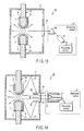
- FIG. 1 is a vertical sectional view of the electric contact apparatus according to the first embodiment, which is denoted by reference numeral 1.
- the electric contact apparatus 1 comprises a pair of electric contacts 2a and 2b, a housing 3, and a measuring section 4. In the electric contact apparatus 1, abrasion of the electric contacts 2a and 2b is detected.
- the distal end portions of the electric contacts 2a and 2b are provided in the housing 3.
- the electric contacts 2a and 2b perform an electrical opening and closing operation for opening and closing an electric circuit.
- the electric contacts 2a and 2b are separated from each other when the electric circuit is in its opened state, and contact each other when the electric circuit is in its closed state.
- the electric contacts 2a and 2b each include a base material portion 5, an indication layer (indication component layer) 6 and a surface processing layer 7.
- the electric contacts 2a and 2b contact each other when the electric circuit is in its closed state.
- the electric contacts 2a and 2b may be formed such that one of them is fitted in the other, when the electric circuit is in its closed state.
- the base material portions 5 provided at the distal ends of the electric contacts 2a and 2b are located to face each other.
- the base material portions 5 each contain metal such as copper (Cu) and aluminum (Al), which is thus conductive.
- the surface processing layers 7 each also contain the same kind of metal as the base material portions 5 or metal such as silver (Ag), which is conductive.
- the surface processing layers 7 are provided on surface sides of the electric contacts 2a and 2b, respectively.
- the indication layers 6 are provided on the outer peripheral surfaces of the base material portions 5.
- the surface layers 7 are provided on the outer peripheral surfaces of the indication layers 6. That is, the indication layers 6 are interposed between the base material portions 5 and the surface processing layers 7.
- the indication layers 6 are located in abrasion detection positions of the electric contacts 2a and 2b.
- the abrasion detection positions are located close to positions where abrasion of the electric contacts 2a and 2b reaches the limit of abrasion.
- the abrasion detection positions are located just before (closer to the surface sides of the electric contacts than) positions where the opening and closing operation of the electric contacts 2a and 2b become abnormal due to mechanical or electrical abrasion of the electric contacts 2a and 2b.
- the boundaries between the indication layers 6 and the surface processing layers 7 correspond to the abrasion detection positions.
- the characteristics e.g., at least one of the wavelength and light intensity
- the characteristics e.g., at least one of the wavelength and light intensity
- the distal end portions of the electric contacts 2a and 2b are located in the housing 3. Also, the distal end portions of the base material portions 5 of the electric contacts 2a and 2b are located in the housing 3.
- the electric contacts 2a and 2b can be opened and closed by a driving device not shown which is located outside the housing 3.
- a measuring section 4 detects light which is generated between the electric contacts 2a and 2b when the electric contacts 2a and 2b are opened and closed, and also detects abrasion of the electric contacts 2a and 2b.
- the measuring section 4 comprises a filter 8, a photosensor 9 and a processing section 10.
- the filter 8 is provided on a light receiving side of the photosensor 9.
- the filter 8 selectively filters light generated as an arc between the electric contacts 2a and 2b at the time of opening and closing thereof, such that a light component of the light which has a given wavelength is transmitted through the filter 8.
- the filter 8 may be formed by selectively combining a number of kinds of filter elements having different wavelength selectivities, so that the light component of light which can be transmitted through the filter 8 varies in accordance with the combination of the filter elements.
- the photosensor 9 measures light generated between the electric contacts 2a and 2b at the time of opening and closing of the electric contacts 2a and 2b, after the light is transmitted through the filter 8. To be more specific, of light generated between electric contacts 2a and 2b, a light component having a given wavelength, which is transmitted through the filter 8, is measured by the photosensor 9. The photosensor 9 converts the measured light component into an electrical signal, and outputs the electrical signal to the processing section 10.
- the filter 8 and the light receiving side of the photosensor 9 are provided close to the electric contacts 2a and 2b. Also, the filter 8 and the light receiving side of the photosensor 9 are located in such a way as to project from the outside of the housing 3 thereinto.
- the photosensor 9 is connected to the processing section 10 located outside the housing 3. That is, the measuring section 4 measures light generated at the electric contacts 2a and 2b at the time of opening and closing thereof, after the light is transmitted through the filter 8, and outputs an electric signal from the photosensor 9 to the processing section located outside the housing 3.
- the processing section 10 receives the electrical signal from the photosensor 9, and records and analyzes the electrical signal. The processing section 10 then carries out abrasion detection by determining whether abrasion of the electric contacts 2a and 2b has reached the abrasion detection positions.
- FIG. 2 is a vertical sectional view with respect to an example of manufacturing steps which are carried out on each of the electric contacts 2a and 2b.
- the indication layer 6 is provided on the outer peripheral surface of the base material portion 5, and is different from the surface processing layer 7 regarding at least one of the wavelength and intensity of generated light.
- the indication layer 6 is formed by applying, e.g., a plating method (such as electroplating, electroless plating or hot dipping) to the outer peripheral surface of the base material portion 5.
- a plating method such as electroplating, electroless plating or hot dipping
- the indication layer 6 may be provided by using a method other than the plating method, such as thermal spraying, raised welding, pressure welding or HIP (Hot Isostatic Pressing) in which heat treatment is carried out while applying a pressure. Also, when each of the electric contacts 2a and 2b is molded, the indication layer 6 may be formed of a clad material in which a component is sandwiched between other components, e.g., copper plates or aluminum plates, which are the same as the component of the surface processing layer 7.
- a method other than the plating method such as thermal spraying, raised welding, pressure welding or HIP (Hot Isostatic Pressing) in which heat treatment is carried out while applying a pressure.
- HIP Het Isostatic Pressing
- the component of the indication layer 6 is metal or alloy, which is different from that of the surface processing layer 7 regarding at least one of the wavelength and intensity of generated light.
- the surface processing layer 7 is provided on the outer peripheral surface of the indication layer 6, and is different from the surface processing layer 6 in at least one of the wavelength and intensity of generated light.
- the component of the surface processing layer 7 may be formed of metal which is the same as that of the base material portion 5 regarding at least one of the wavelength and intensity of generated light or high conductive material such as Ag.
- the indication layer 6 is covered by the surface processing layer 7.
- the electric contacts 2a and 2b are formed such that the indication layers 6 are interposed between the base material portions 6 and the surface processing layers 7, i.e., the indication layers 6 are located in the abrasion detection positions.
- the electric contacts 2a and 2b are formed of a component to which the plating method cannot be applied, or of alloy containing a component to which the plating method cannot be applied, their formation is carried out by thermal spraying, raised welding, pressure welding, HIP or cladding.
- the indication layer 6 is formed of a component which is different in emission spectrum from a component widely used in electrodes, and a component which is different in a component, e.g., silver, aluminum or copper, which is the same as the component of the surface processing layer 7.
- the component of the indication layer 6 does not overlap with that of the surface processing layer 7 in emission spectrum.
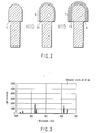
- FIG. 3 is a graph showing an emission spectrum of Ag which is the first example of the component of the surface processing layer 7.
- FIG. 4 is a graph showing an emission spectrum of Al which is the second example of the component of the surface processing layer 7.
- FIG. 5 is a graph showing an emission spectrum of Cu which is the third example of the component of the surface processing layer 7.
- the representative examples of the component of the surface processing layer 7 have characteristics in which the intensities of light generated from them do not have a peak at approximately from 400 nm to 500 nm.
- a component from which light having a high intensity at approximately from 400 nm to 500 nm is generated is suitable as the component of the indication layer 6.
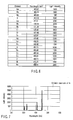
- FIG. 6 shows a list of elements each suitable as the component of the indication layer 6, and having characteristics in which the intensities of light generated from the elements are high at approximately from 400 nm to 500 nm.
- Ba (approximately 455 nm), Bi (approximately 472 nm), Cs (approximately 459 nm), Eu (approximately 459 nm), Fe (approximately 440 nm), Ga (approximately 417 nm), Hg (approximately 435 nm), La (approximately 433 nm), Li (approximately 460 nm), Nb (approximately 405 nm), Pb (approximately 405 nm), Rb (approximately 420 nm), Re (approximately 488 nm) and Sr (approximately 460 nm) are each suitable as the component of the indication layer 6, since the intensities of light generated from those elements are high at approximately from 400 nm to 500 nm.
- the electric contacts 2a and 2b may be formed of an appropriate one of various kinds of alloys.
- FIG. 7 is a graph showing an emission spectrum of indium (In) which is an example of the component of the indication layer 6.
- Light generated from indium has a high intensity at a wavelength of approximately 410 nm and that of approximately 451 nm.
- the indication layers 6 including indium are located in abrasion detection positions of the electric contacts 2a and 2b.
- the filter 8 cuts light of a wavelength of approximately less than 400 nm and that of approximately more than 500 nm which is generated at the electric contacts 2a and 2b at the time of opening and closing thereof.
- the photosensor 9 measures intensity of the light transmitted through the filter 8.
- the processing section 10 judges whether or not a measuring result is included in a given range.
- the electric contact apparatus 1 can detect that abrasion of the electric contacts 2a and 2b.
- chromium cr
- indium light generated from chromium can be clearly observed at approximately 428 nm.
- tin (Sn) and zinc (Zn) may be each used as the component of the indication layer 6.
- the emission characteristics of the electric contacts 2a and 2b at the time of opening and closing thereof vary, and it can be thus directly detected that abrasion of the surface processing layer 7 of the electric contacts 2a and 2b reaches the abrasion detection positions.
- abrasion of the electric contacts 2a and 2b can be detected before the limit of abrasion, and monitoring and maintenance of electric contacts 2a and 2b can thus be easily carried out.
- the accurate operations of electric contacts 2a and 2b can be guaranteed, and the security and reliability and each of an electric device and an electric equipment can be improved.
- light transmitted through the filter 8 is measured by the photosensor 9, as a result of which only light having a given wavelength can be measured, and the accuracy of abrasion detection can be improved.
- the measurement precision of the photosensor 9 is improved, as compared with the conventional apparatus or method.
- the filter 8 is a combination of various kinds of filter elements having different wavelength selectivities, and the wavelength of light to be transmitted through the filter 8 can be further finely limited by the filter 8.
- the second embodiment will be explained as a modification of the first embodiment.
- surface processing layers are provided on distal end portions of base material portions, and abrasion is detected when light emission at the opening and closing time of the electric contacts is changed from light emission of the surface processing layers to that of the base material portions.
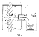
- FIG. 8 is a vertical sectional view of an example of an electric contact apparatus according to second embodiment of the present invention, which is denoted by reference numeral 11.
- the electric contact apparatus 11 comprises the electric contacts 12a and 12b, the housing 3 and a measuring section 13.
- the electric contacts 12a and 12b comprise base material portions 14 and surface processing layers 15.
- the boundaries between the base material portions 14 and the surface processing layers 15 serve as abrasion detection positions.
- the characteristics of light which is generated from the base material portions 14 at the time of opening and closing of the electric contacts 12a and 12b when abrasion of the surface processing layers 15 reach the abrasion detection positions are different from those of light generated from the surface processing layers 15 at the time of opening and closing of the electric contacts 12a and 12b.
- the distal end portions of the electric contacts 12a and 12b are located in the housing 3.
- the electric contacts 12a and 12b can be opened and closed by a driving device not shown which is located outside.
- the surface processing layers 15 contain conductive material, and can be operated as electrodes.
- the measuring section 13 comprises a filter 16, a photosensor 9 and a processing section 17.
- the filters 16 allow light having a given wavelength to be transmitted through the filters 16.
- light having a given wavelength which is transmitted through the filter 16 is measured by the photosensor 9.
- the photosensor 9 converts the measured light into an electrical signal, and outputs the electrical signal to the processing section 17.
- the processing section 17 detects abrasion of the electric contacts 12a and 12b based on variation of the characteristics of the light.
- the surface processing layers 15 contain silver, it is detected that light generated from the surface processing layers 15 has a high intensity at approximately 330 nm, 520 nm and 550 nm as shown in FIG. 3.
- the processing section 17 detects light generated from the material of the base material portions 14, to thereby detect the difference between the spectrums of light which are obtained before and after abrasion of the surface processing layers 15.
- the surface processing layers 15 are formed on the outer peripheral surfaces of the base material portions 14 by a plating method, even if any of, e.g., electroplating, electroless plating and hot dipping is applied as the plating method, the surface processing layers 15 can be formed to have a given thickness which falls within an allowable range set for abrasion, and is substantially equal to those obtained when the other plating methods are applied.
- the emission characteristics thereof at the time of opening and closing of the electric contacts 12a and 12b vary, as a result of which it can be directly detected that abrasion of the surface processing layers 15 reaches the abrasion detection positions.
- the third embodiment will be explained as another modification of the first embodiment.
- holes are formed in the distal end portions of base material portions, indication portions are provided in abrasion detection positions in the holes, and the holes are covered with caps.
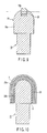
- FIG. 9 is a vertical sectional view of an example of electric contacts in the third embodiment.
- electric contacts 18 comprise base material portions 19 and indication portions 20.
- the base material portions 19 comprise base material bodies 19a and caps 19b.
- the indication portions 20 are provided in the base material bodies 19a of the base material portions 19 at the distal ends of the electric contacts 18. In the holes, the indication portions 20 are provided. The caps 19b close opening portions of the holes. As a result, the indication portions 20 are held in the base material portions 19. The boundaries between the caps 19b and the indication portions 20 serve as the abrasion detection positions. The indication portions 20 are mechanically fixed to, e.g., the abrasion detection positions, and also fixed by the caps 19b from above.
- the base material bodies 19a screw holes are formed, and then metal pieces containing components which can effect indication are screwed as the indication portions 20 in the abrasion detection positions. Furthermore, the caps 19b whose components are the same as those of the base material bodies 19a are also screwed, and then fixed by welding or the like. Then, the shapes of the base material portions 19 are corrected by machining or the like. Thereby, the indication portions 20 are embedded in the abrasion detection positions of the base material portions 19.
- the base material portions 19 each contain a component such as silver, aluminum or copper.
- the indication portions 20, at the time of opening and closing of the electric contacts 18, generate light the wavelength of which is different from that of light generated from the base material portions 19, when they are located at the surfaces of the electric contacts 18.
- the characteristics of light generated by the opening and closing operations vary when abrasion of the electric contacts 18 progresses due to the opening and closing operation thereof, and reaches the abrasion detection positions.
- the fourth embodiment will be explained as a further modification of the first embodiment.
- each of electric contacts includes a number of indication layers in a number of abrasion detection positions indicating abrasion different levels.
- FIG. 10 is a vertical sectional view of an example of electric contacts in the fourth embodiment of the present invention.
- electric contacts 21 have multi-layer structures, and comprise base material portions 5, first indication layers 22a, second indication layers 22b, intermediate layers 23 and surface processing layers 7.
- the second indication layers 22b are provided on the outer peripheral surfaces of the base material portions 19 provided at the distal ends of the electric contacts.
- the intermediate layers 23 are provided on the outer peripheral surfaces of the second indication layers 22b.
- the first indication layers 22a are provided on the outer peripheral surfaces of the intermediate layers 23.
- the surface processing layers 7 are provided on the outer peripheral surfaces of the first indication layers 22a.
- the boundaries between the surface processing layers 7 and the first indication layers 22a serve as first abrasion detection positions.
- the boundaries between the intermediate layers 23 and the second indication layers 22b serve as second abrasion detection positions.
- the base material layers 5, the intermediate layers 23 and the surface processing layers 7 contain any of silver, aluminum and copper, etc.
- each of the first indication layers 22a and the second indication layers 22b When the first indication layers 22a and the second indication layers 22b are exposed at the surfaces of the electric contacts 21 at the time of opening and closing thereof, each of the first indication layers 22a and the second indication layers 22b generates light having a wavelength differing from that of light generated from layers adjacent to each of the first indication layers 22a and the second indication layers 22b.
- the above layers adjacent to the first indication layers 22a are the surface processing layers 7 and the intermediate layers 23.
- the layers adjacent to the second indication layers 22b are intermediate layers 23.
- the first indication layers 22a contain chromium
- the second indication layers 22b contain indium.
- the above light having a wavelength of approximately 428 nm which is generated from chromium reduces, and light having a wavelength of approximately 410 and a wavelength of approximately 450 nm which is generated from indium of the second indication layers 22b is measured.
- first indication layers 22a and the second indication layers 22b can be used as the components of the first indication layers 22a and the second indication layers 22b by using thermal spraying, raised welding, pressure welding or cladding.
- the electric contacts 21 have multi-layer structures.
- conductive materials of which the surface processing layers are formed abrade, and then the surfaces of the first indication layers 22 appear. Consequently, at the time of the opening and closing operation, light which is generated from the first indication layers 22a, and is characteristic thereof is generated.
- the abraded states of the electric contacts 21 can be detected in stages.
- An electric contact apparatus includes a housing 3 provided with a window.
- the window can be also applied to the second to fourth embodiments.
- FIG. 11 is a vertical sectional view of an example of a structure wherein the window is provided in the housing, according to the fifth embodiment.
- windows 24 are fixed to the housing 3 by, e.g., flange.
- Light generated between the electric contacts 2a and 2b at the time of opening and closing thereof can be measured from the outside of the housing 3, after passing through the windows 24 located in arbitrary positions of the housing 3.
- the windows 24 may be provided in positions where light generated between the electric contacts 2a and 2b at the time of opening and closing thereof is directly transmitted through the windows 24 or where the light is indirectly transmitted through the windows 24, i.e., it is transmitted therethrough after being reflected.
- FIG. 12 is a vertical sectional view of the first example of the electric contact apparatus according to the fifth embodiment, which is denoted by reference numeral 25.
- the electric contact apparatus 25 light generated between the electric contacts 2a and 2b at the time of opening and closing thereof is measured by the photosensor 9 through the window 24 and the filter 8.
- the measuring section 4 is provided outside the housing 3.
- FIG. 13 is a vertical sectional view of the second example of the electric contact apparatus according to the fifth embodiment, which is denoted by reference numeral 26.
- a measuring section 27 of the electric contact apparatus 26 comprises a wavelength dispersing section 28 such as a prism, the photosensor 9, and the' processing section 10.
- the wavelength dispersing section 28 receives light generated between the electric contacts 2a and 2b at the time of opening and closing thereof through the window 24, and disperses the light in wavelength, and outputs only a light component of the light which has a given wavelength or an emission spectrum of a given wavelength range to the photosensor 9.
- the light generated between the electric contacts 2a and 2b at the time of opening and closing thereof is measured by the photosensor 9 through the window 24 and the wavelength dispersing section 28.
- the measuring section 27 is provided outside the housing 3.
- abrasion of the electric contacts 2a and 2b is easily detected by using not only a dedicated light measuring device such as the measuring section 4, but a device such as the measuring section 27, which has a measuring function differing from that of the measuring section 4, as occasion arises.
- the sixth embodiment will be explained as a modification of the fifth embodiment.
- the electric contact apparatus which is denoted by reference numeral 29, comprises a light-direction adjusting section 30 which is provided in the window 24, and which includes light transmission holes for adjusting the direction of light generated at the time of opening and closing of the electric contacts 2a and 2b.
- FIG. 14 is a vertical sectional view of an example of the electric contact apparatus 29 according to the sixth embodiment of the present invention.
- the window 24 allows the light generated between the electric contacts 2a and 2b at the time of 'opening and closing thereof to be transmitted through the window 24, and is provided at a side surface of the housing 3 which is parallel to a direction in which the electric contacts 2a and 2b are opened/closed.
- the light-direction adjusting section 30 is provided at the window 24.
- the light-direction adjusting section 30 is a stray-light removing mechanism which is formed in the shape of an optical grating or slits in such a way as to project into the housing 3.
- the light-direction adjusting section 30 allows only directly incident light components L1 and L2 of the light generated between the electric contacts 2a and 2b at the time of opening and closing thereof to be transmitted through the light-direction adjusting section 30, but does not allow stray light components L3 and L4 of the light to be transmitted through the light-direction adjusting section 30.
- the light-direction adjusting section 30 is painted black so as to allow only the light components L1 and L2 to be transmitted through the light-direction adjusting section 30, and so as to absorb the other light components.
- plural plates are provided in parallel with the light components L1 and L2.
- appropriate absorption material 31 for absorbing a decomposition product generated due to discharge may be provided as shown in FIG. 15.
- the seventh embodiment will be explained as a modification of a combination of the first and second embodiments.
- the seventh embodiment is given with respect to the case where an optical fiber is applied to the first embodiment.
- the optical fiber can be applied to any of the other embodiments.
- FIG. 16 is a vertical sectional view of an example of the electric contact apparatus 32 according to the seventh embodiment.
- one (light receiving portion) of the ends of an optical fiber 33 is located close to the electric contacts 2a and 2b within the housing 3, and the other is located outside the housing 3.
- the optical fiber 33 receives light generated between the electric contacts 2a and 2b at the time of opening and closing thereof, and guides the light to the other end.
- the measuring section 4 located outside the housing 3 measures the light output from the other end of the optical fiber 33, to thereby perform abrasion detection.
- the optical fiber 33 is provided to extend from the inside of the housing 3 to the outside thereof, and the other end of the optical fiber 33 is connected to the measuring section 4.
- light generated between the electric contacts 2a and 2b at the time of opening and closing thereof can be measured in an arbitrary position in the outside of the housing 3 through the optical fiber 3, and abrasion of the electric contacts 2a and 2b can be detected in the arbitrary position.
- the optical fiber 33 can be formed to have characteristics which prevents transmission of ultraviolet rays.
- a filter for blocking a light component of shortwave can be omitted.
- a plurality of optical fibers 33 are provided such that one end of each of the optical fibers 33 is located close to an associated pair of electric contacts 2a and 2b of the plurality of pairs of electric contacts 2a and 2b. That is, the optical fibers 33 are provided to extend from the inside of the housing 3 to the outside thereof for the pairs of electric contacts 2a and 2b, respectively. The other end of each optical fiber 33 is connected to an associated one of a plurality of measuring sections 4.
- abrasion detection can be performed in units of one pair of electric contacts 2a and 2b.
- the measuring sections 4 do not need to be located close to the housing 3, and can be concentratively provided in a certain place, thus reducing the restrictions on the entire structure of the electric contact apparatus and the arrangement of the structural elements thereof.
- the optical fibers 33 respectively located close to the pairs of electric contacts 2a and 2b may be bundled and connected to one measuring section 4.
- the pairs of the electric contacts 2a and 2b can be concentratively monitored by one measuring section 4.
- any of the pairs of electric contacts 2a and 2b, 12a and 12b, 18, and 21 can be applied to each of the electric contact apparatuses 1, 11, 25, 26, 29 and 32.
- each of the indication layer 6, the first indication layer 22a, the second indication 22b and the indication portion 20 can be formed of any of metal, alloy and a luminiferous material.
- the indication layers 6, 6 of the two electric contacts 2a and 2b may be made of different two metals, respectively. That is, the composition of the indication layer 6 of the electric contact 2a, along with the description of each embodiment, may be different from that of the electric contact 2b. In this case, it can be detected which one of the electric contacts reaches the abrasion detection position if the abrasion is asymmetrical.
- each element may be freely modified, its place may be changed to another place, the elements may be freely selectively combined, and each of them may be divided into parts.
Landscapes
- Contacts (AREA)
- Gas-Insulated Switchgears (AREA)
- High-Tension Arc-Extinguishing Switches Without Spraying Means (AREA)
- Measurement Of Length, Angles, Or The Like Using Electric Or Magnetic Means (AREA)
Applications Claiming Priority (2)
| Application Number | Priority Date | Filing Date | Title |
|---|---|---|---|
| JP2003298103 | 2003-08-22 | ||
| JP2003298103A JP4334299B2 (ja) | 2003-08-22 | 2003-08-22 | 電気接点、電気接点摩耗検出装置およびその摩耗検出方法 |
Publications (3)
| Publication Number | Publication Date |
|---|---|
| EP1508908A2 true EP1508908A2 (fr) | 2005-02-23 |
| EP1508908A3 EP1508908A3 (fr) | 2007-04-04 |
| EP1508908B1 EP1508908B1 (fr) | 2014-02-19 |
Family
ID=34056256
Family Applications (1)
| Application Number | Title | Priority Date | Filing Date |
|---|---|---|---|
| EP04019801.2A Expired - Lifetime EP1508908B1 (fr) | 2003-08-22 | 2004-08-20 | Contacts électriques et appareil électrique pour la détection d'usure des contacts électriques |
Country Status (3)
| Country | Link |
|---|---|
| US (1) | US7049532B2 (fr) |
| EP (1) | EP1508908B1 (fr) |
| JP (1) | JP4334299B2 (fr) |
Cited By (3)
| Publication number | Priority date | Publication date | Assignee | Title |
|---|---|---|---|---|
| US7217615B1 (en) | 2000-08-31 | 2007-05-15 | Micron Technology, Inc. | Capacitor fabrication methods including forming a conductive layer |
| EP1895554A1 (fr) * | 2006-09-04 | 2008-03-05 | ABB Research Ltd | Contact électrique avec une zone de signalisation pour signaler l'usage de contact |
| WO2009132610A1 (fr) * | 2008-04-29 | 2009-11-05 | Vogl Electronic Gmbh | Système et procédé de diagnostic de l’état opérationnel technique d’un commutateur de puissance |
Families Citing this family (16)
| Publication number | Priority date | Publication date | Assignee | Title |
|---|---|---|---|---|
| US7579581B2 (en) * | 2006-05-19 | 2009-08-25 | Siemens Energy & Automation, Inc. | System for optically detecting an electrical arc in a power supply |
| JP5032091B2 (ja) | 2006-10-12 | 2012-09-26 | 株式会社東芝 | ガス絶縁開閉装置及びガス絶縁開閉装置用部品のアーク損傷検出方法 |
| US7705744B2 (en) * | 2007-05-24 | 2010-04-27 | Cutsforth Products, Inc. | Monitoring systems and methods for monitoring the condition of one or more components of an electrical device |
| US8618943B2 (en) | 2007-05-24 | 2013-12-31 | Cutsforth, Inc. | Brush holder assembly monitoring apparatus, assembly, system and method |
| JP5893838B2 (ja) * | 2011-03-18 | 2016-03-23 | 新光電気工業株式会社 | 放熱部品及びそれを有する半導体パッケージ、放熱部品の製造方法 |
| US9329238B1 (en) * | 2014-11-14 | 2016-05-03 | Schneider Electric USA, Inc. | Contact wear detection by spectral analysis shift |
| JP6442292B2 (ja) * | 2015-01-07 | 2018-12-19 | 西日本旅客鉄道株式会社 | パンタグラフ異常検知システム |
| CA2985094C (fr) | 2015-06-01 | 2022-03-22 | Cutsforth, Inc. | Surveillance de l'usure et des vibrations d'un balai |
| CA3008957C (fr) | 2016-01-11 | 2020-07-14 | Cutsforth, Inc. | Systeme de controle destine a un appareil de mise a la terre |
| JP2018032583A (ja) * | 2016-08-26 | 2018-03-01 | パナソニックIpマネジメント株式会社 | 接点装置、接点装置に用いられる収納容器および接点装置を搭載した電磁継電器 |
| KR102026827B1 (ko) * | 2018-03-27 | 2019-09-30 | 두산중공업 주식회사 | 가스 터빈 및 그 모니터링 시스템 |
| CN113243063B (zh) | 2018-10-04 | 2023-11-07 | 科茨福斯有限公司 | 用于监控电机的一个或多个元件的状态的系统和方法 |
| CA3114764A1 (fr) | 2018-10-04 | 2020-04-09 | Cutsforth, Inc. | Systeme et procede de surveillance de l'etat d'un ou de plusieurs composants d'une machine electrique |
| WO2020204397A1 (fr) * | 2019-04-05 | 2020-10-08 | 엘에스일렉트릭(주) | Dispositif de surveillance de point de contact pour disjoncteur à vide, et procédé de correction réalisé à l'aide dudit dispositif |
| EP4030456B1 (fr) * | 2019-09-10 | 2025-12-03 | Ls Electric Co., Ltd. | Dispositif de surveillance de contact pour disjoncteur à vide, et disjoncteur à vide le comprenant |
| US11874314B2 (en) * | 2022-02-09 | 2024-01-16 | Caterpillar Inc. | Electrical contact wear monitoring system |
Family Cites Families (10)
| Publication number | Priority date | Publication date | Assignee | Title |
|---|---|---|---|---|
| JPS595512A (ja) * | 1982-06-30 | 1984-01-12 | 松下電工株式会社 | 接点材料 |
| JPS60198011A (ja) * | 1984-03-22 | 1985-10-07 | 日新電機株式会社 | 接点寿命監視装置 |
| US4553008A (en) * | 1984-06-14 | 1985-11-12 | Cooper Industries, Inc. | Load interrupter |
| US4723084A (en) * | 1986-11-13 | 1988-02-02 | General Electric Company | Light conductor brush wear detector assembly |
| JPH0614501B2 (ja) | 1990-06-20 | 1994-02-23 | 太陽誘電株式会社 | 磁器コンデンサ及びその製造方法 |
| EP0788598B1 (fr) * | 1994-10-30 | 1998-04-01 | Tiede Gmbh + Co Rissprüfanlagen | Appareil pour le controle d'une suspension d'un materiau susceptible de fluorescence |
| US5718581A (en) * | 1995-05-09 | 1998-02-17 | Danville Manufacturing, Inc. | Air abrasive particle apparatus |
| JPH10241481A (ja) | 1997-02-21 | 1998-09-11 | Matsushita Electric Works Ltd | 電磁継電器 |
| JPH11354341A (ja) | 1998-06-11 | 1999-12-24 | Toshiba Corp | 負荷時タップ切換器の監視装置 |
| US6777948B2 (en) * | 2002-09-11 | 2004-08-17 | Electric Power Research Institute, Inc. | Method and apparatus for detecting wear in components of high voltage electrical equipment |
-
2003
- 2003-08-22 JP JP2003298103A patent/JP4334299B2/ja not_active Expired - Fee Related
-
2004
- 2004-08-19 US US10/921,209 patent/US7049532B2/en not_active Expired - Fee Related
- 2004-08-20 EP EP04019801.2A patent/EP1508908B1/fr not_active Expired - Lifetime
Non-Patent Citations (1)
| Title |
|---|
| None |
Cited By (3)
| Publication number | Priority date | Publication date | Assignee | Title |
|---|---|---|---|---|
| US7217615B1 (en) | 2000-08-31 | 2007-05-15 | Micron Technology, Inc. | Capacitor fabrication methods including forming a conductive layer |
| EP1895554A1 (fr) * | 2006-09-04 | 2008-03-05 | ABB Research Ltd | Contact électrique avec une zone de signalisation pour signaler l'usage de contact |
| WO2009132610A1 (fr) * | 2008-04-29 | 2009-11-05 | Vogl Electronic Gmbh | Système et procédé de diagnostic de l’état opérationnel technique d’un commutateur de puissance |
Also Published As
| Publication number | Publication date |
|---|---|
| JP2005071727A (ja) | 2005-03-17 |
| US7049532B2 (en) | 2006-05-23 |
| EP1508908B1 (fr) | 2014-02-19 |
| US20050040020A1 (en) | 2005-02-24 |
| JP4334299B2 (ja) | 2009-09-30 |
| EP1508908A3 (fr) | 2007-04-04 |
Similar Documents
| Publication | Publication Date | Title |
|---|---|---|
| US7049532B2 (en) | Electric contacts, electric contact apparatus and method for detecting abrasion of the electric contacts | |
| JP5571782B2 (ja) | アーク閃光検出システム | |
| EP3234929B1 (fr) | Dispositif et procédé pour contrôler des substances caractéristiques | |
| EP0249815A1 (fr) | Dispositif pour la détection d'arcs de défaut | |
| CN105575725A (zh) | 一种真空开关中真空灭弧室的真空度在线监测装置及方法 | |
| US20190101521A1 (en) | Diagnosing Device for On-Load Tap Changing Apparatus, Diagnosing Method for On-Load Tap Changing Apparatus, and Diagnosing Device for Transformer | |
| CN119891561B (zh) | 升压站监控运维系统 | |
| US7408357B2 (en) | Device for detecting contact wear in switching appliances | |
| CA2498775C (fr) | Procede et dispositif de detection d'usure dans des composants d'appareillages electriques haute tension | |
| CN114341591A (zh) | 真空断路器用触点监视装置及具有其的真空断路器 | |
| US20040113070A1 (en) | Method and apparatus for determining electrical contact wear | |
| CN121091058A (zh) | 一种低压断路器的灭弧装置寿命预测方法 | |
| EP0415370B2 (fr) | Appareil de puissance, unité de transmission de puissance ou de distribution et procédé de déclenchement à cet effet | |
| EP2314197A1 (fr) | Élément optique, élément spectroscopique, unité optique et dispositif optique | |
| DE102013114171B4 (de) | Schaltkammer zum Führen und Trennen von elektrischen Strömen mittels beweglicher Schaltkontakte | |
| EP0103921B1 (fr) | Equipement de haute tension avec enregistrement de lumière perturbante | |
| EP0040918A1 (fr) | Un interrupteur à vide avec un système de contrôle de pression | |
| JP4156455B2 (ja) | 多色式光学膜厚計測装置及び方法 | |
| DE102021209975A1 (de) | Vakuumschaltanordnung und Verfahren zum Erkennen eines Lichtbogens | |
| EP4369372A1 (fr) | Interrupteur à vide, agencement de transformateur et procédé de surveillance d'interrupteur à vide | |
| JP2022089419A (ja) | アーク光検出装置、アーク光検出装置および電気設備を備える装置、ならびにアーク光検出方法 | |
| US4315116A (en) | Switch assembly with leakage current detecting means | |
| HK1095201B (en) | Device for detecting contact wear in switching appliances | |
| KR20240111541A (ko) | 변전기기 예방진단 시스템을 이용한 변전설비 상태 진단 방법 | |
| CN121461147A (zh) | 一种低压抽出式开关柜的智能运维方法、系统、介质及产品 |
Legal Events
| Date | Code | Title | Description |
|---|---|---|---|
| PUAI | Public reference made under article 153(3) epc to a published international application that has entered the european phase |
Free format text: ORIGINAL CODE: 0009012 |
|
| 17P | Request for examination filed |
Effective date: 20040820 |
|
| AK | Designated contracting states |
Kind code of ref document: A2 Designated state(s): AT BE BG CH CY CZ DE DK EE ES FI FR GB GR HU IE IT LI LU MC NL PL PT RO SE SI SK TR |
|
| AX | Request for extension of the european patent |
Extension state: AL HR LT LV MK |
|
| RAP1 | Party data changed (applicant data changed or rights of an application transferred) |
Owner name: KABUSHIKI KAISHA TOSHIBA |
|
| PUAL | Search report despatched |
Free format text: ORIGINAL CODE: 0009013 |
|
| AK | Designated contracting states |
Kind code of ref document: A3 Designated state(s): AT BE BG CH CY CZ DE DK EE ES FI FR GB GR HU IE IT LI LU MC NL PL PT RO SE SI SK TR |
|
| AX | Request for extension of the european patent |
Extension state: AL HR LT LV MK |
|
| AKX | Designation fees paid |
Designated state(s): DE FR |
|
| 17Q | First examination report despatched |
Effective date: 20110119 |
|
| GRAP | Despatch of communication of intention to grant a patent |
Free format text: ORIGINAL CODE: EPIDOSNIGR1 |
|
| INTG | Intention to grant announced |
Effective date: 20130819 |
|
| GRAS | Grant fee paid |
Free format text: ORIGINAL CODE: EPIDOSNIGR3 |
|
| GRAA | (expected) grant |
Free format text: ORIGINAL CODE: 0009210 |
|
| AK | Designated contracting states |
Kind code of ref document: B1 Designated state(s): DE FR |
|
| REG | Reference to a national code |
Ref country code: DE Ref legal event code: R096 Ref document number: 602004044410 Country of ref document: DE Effective date: 20140403 |
|
| REG | Reference to a national code |
Ref country code: DE Ref legal event code: R097 Ref document number: 602004044410 Country of ref document: DE |
|
| PLBE | No opposition filed within time limit |
Free format text: ORIGINAL CODE: 0009261 |
|
| STAA | Information on the status of an ep patent application or granted ep patent |
Free format text: STATUS: NO OPPOSITION FILED WITHIN TIME LIMIT |
|
| 26N | No opposition filed |
Effective date: 20141120 |
|
| REG | Reference to a national code |
Ref country code: DE Ref legal event code: R097 Ref document number: 602004044410 Country of ref document: DE Effective date: 20141120 |
|
| REG | Reference to a national code |
Ref country code: FR Ref legal event code: PLFP Year of fee payment: 12 |
|
| PGFP | Annual fee paid to national office [announced via postgrant information from national office to epo] |
Ref country code: DE Payment date: 20150811 Year of fee payment: 12 |
|
| PGFP | Annual fee paid to national office [announced via postgrant information from national office to epo] |
Ref country code: FR Payment date: 20150629 Year of fee payment: 12 |
|
| REG | Reference to a national code |
Ref country code: DE Ref legal event code: R119 Ref document number: 602004044410 Country of ref document: DE |
|
| REG | Reference to a national code |
Ref country code: FR Ref legal event code: ST Effective date: 20170428 |
|
| PG25 | Lapsed in a contracting state [announced via postgrant information from national office to epo] |
Ref country code: DE Free format text: LAPSE BECAUSE OF NON-PAYMENT OF DUE FEES Effective date: 20170301 Ref country code: FR Free format text: LAPSE BECAUSE OF NON-PAYMENT OF DUE FEES Effective date: 20160831 |