EP1504460B1 - Improved electrode for thin film capacitor devices - Google Patents
Improved electrode for thin film capacitor devices Download PDFInfo
- Publication number
- EP1504460B1 EP1504460B1 EP03734002A EP03734002A EP1504460B1 EP 1504460 B1 EP1504460 B1 EP 1504460B1 EP 03734002 A EP03734002 A EP 03734002A EP 03734002 A EP03734002 A EP 03734002A EP 1504460 B1 EP1504460 B1 EP 1504460B1
- Authority
- EP
- European Patent Office
- Prior art keywords
- electrode
- layer
- platinum
- tantalum
- ferroelectric
- Prior art date
- Legal status (The legal status is an assumption and is not a legal conclusion. Google has not performed a legal analysis and makes no representation as to the accuracy of the status listed.)
- Expired - Lifetime
Links
- 239000010409 thin film Substances 0.000 title claims abstract description 13
- 239000003990 capacitor Substances 0.000 title claims abstract description 12
- 238000000034 method Methods 0.000 claims abstract description 38
- 239000000758 substrate Substances 0.000 claims abstract description 16
- 239000004020 conductor Substances 0.000 claims abstract description 14
- 239000011521 glass Substances 0.000 claims abstract description 14
- 229910000510 noble metal Inorganic materials 0.000 claims abstract description 11
- PBCFLUZVCVVTBY-UHFFFAOYSA-N tantalum pentoxide Inorganic materials O=[Ta](=O)O[Ta](=O)=O PBCFLUZVCVVTBY-UHFFFAOYSA-N 0.000 claims abstract description 10
- BASFCYQUMIYNBI-UHFFFAOYSA-N platinum Chemical compound [Pt] BASFCYQUMIYNBI-UHFFFAOYSA-N 0.000 claims description 89
- 229910052697 platinum Inorganic materials 0.000 claims description 41
- 230000008021 deposition Effects 0.000 claims description 13
- BPUBBGLMJRNUCC-UHFFFAOYSA-N oxygen(2-);tantalum(5+) Chemical compound [O-2].[O-2].[O-2].[O-2].[O-2].[Ta+5].[Ta+5] BPUBBGLMJRNUCC-UHFFFAOYSA-N 0.000 claims description 12
- 229910052751 metal Inorganic materials 0.000 claims description 11
- 239000002184 metal Substances 0.000 claims description 11
- 230000003647 oxidation Effects 0.000 claims description 11
- 238000007254 oxidation reaction Methods 0.000 claims description 11
- QVGXLLKOCUKJST-UHFFFAOYSA-N atomic oxygen Chemical compound [O] QVGXLLKOCUKJST-UHFFFAOYSA-N 0.000 claims description 9
- 229910052760 oxygen Inorganic materials 0.000 claims description 9
- 239000001301 oxygen Substances 0.000 claims description 9
- KDLHZDBZIXYQEI-UHFFFAOYSA-N Palladium Chemical compound [Pd] KDLHZDBZIXYQEI-UHFFFAOYSA-N 0.000 claims description 6
- 229910044991 metal oxide Inorganic materials 0.000 claims description 6
- 150000004706 metal oxides Chemical class 0.000 claims description 6
- 229910052763 palladium Inorganic materials 0.000 claims description 4
- PCHJSUWPFVWCPO-UHFFFAOYSA-N gold Chemical compound [Au] PCHJSUWPFVWCPO-UHFFFAOYSA-N 0.000 claims description 2
- 229910052737 gold Inorganic materials 0.000 claims description 2
- 239000010931 gold Substances 0.000 claims description 2
- 229910052703 rhodium Inorganic materials 0.000 claims description 2
- 239000010948 rhodium Substances 0.000 claims description 2
- MHOVAHRLVXNVSD-UHFFFAOYSA-N rhodium atom Chemical compound [Rh] MHOVAHRLVXNVSD-UHFFFAOYSA-N 0.000 claims description 2
- 238000010438 heat treatment Methods 0.000 claims 2
- GUVRBAGPIYLISA-UHFFFAOYSA-N tantalum atom Chemical compound [Ta] GUVRBAGPIYLISA-UHFFFAOYSA-N 0.000 abstract description 21
- 229910052715 tantalum Inorganic materials 0.000 abstract description 18
- 238000000151 deposition Methods 0.000 abstract description 15
- 230000001590 oxidative effect Effects 0.000 abstract description 5
- 239000010410 layer Substances 0.000 description 61
- 235000012431 wafers Nutrition 0.000 description 23
- 230000008569 process Effects 0.000 description 21
- 239000010408 film Substances 0.000 description 12
- 239000010936 titanium Substances 0.000 description 11
- 239000000463 material Substances 0.000 description 10
- VYPSYNLAJGMNEJ-UHFFFAOYSA-N Silicium dioxide Chemical compound O=[Si]=O VYPSYNLAJGMNEJ-UHFFFAOYSA-N 0.000 description 8
- 229910052454 barium strontium titanate Inorganic materials 0.000 description 8
- 229910052719 titanium Inorganic materials 0.000 description 8
- 230000015556 catabolic process Effects 0.000 description 7
- RTAQQCXQSZGOHL-UHFFFAOYSA-N Titanium Chemical compound [Ti] RTAQQCXQSZGOHL-UHFFFAOYSA-N 0.000 description 6
- 229910052814 silicon oxide Inorganic materials 0.000 description 6
- XUIMIQQOPSSXEZ-UHFFFAOYSA-N Silicon Chemical compound [Si] XUIMIQQOPSSXEZ-UHFFFAOYSA-N 0.000 description 5
- 238000010586 diagram Methods 0.000 description 5
- 239000011229 interlayer Substances 0.000 description 5
- 229910052710 silicon Inorganic materials 0.000 description 5
- 239000010703 silicon Substances 0.000 description 5
- 238000012360 testing method Methods 0.000 description 5
- GWEVSGVZZGPLCZ-UHFFFAOYSA-N Titan oxide Chemical compound O=[Ti]=O GWEVSGVZZGPLCZ-UHFFFAOYSA-N 0.000 description 4
- 238000012545 processing Methods 0.000 description 4
- 230000001464 adherent effect Effects 0.000 description 3
- 239000000919 ceramic Substances 0.000 description 3
- 238000001704 evaporation Methods 0.000 description 3
- 229910052451 lead zirconate titanate Inorganic materials 0.000 description 3
- 150000002739 metals Chemical class 0.000 description 3
- 230000035945 sensitivity Effects 0.000 description 3
- 229910001936 tantalum oxide Inorganic materials 0.000 description 3
- 229910010252 TiO3 Inorganic materials 0.000 description 2
- VNSWULZVUKFJHK-UHFFFAOYSA-N [Sr].[Bi] Chemical compound [Sr].[Bi] VNSWULZVUKFJHK-UHFFFAOYSA-N 0.000 description 2
- 230000004888 barrier function Effects 0.000 description 2
- 230000015572 biosynthetic process Effects 0.000 description 2
- 229910052804 chromium Inorganic materials 0.000 description 2
- 238000001816 cooling Methods 0.000 description 2
- 238000002425 crystallisation Methods 0.000 description 2
- 230000008025 crystallization Effects 0.000 description 2
- 230000008020 evaporation Effects 0.000 description 2
- 238000010304 firing Methods 0.000 description 2
- 238000004518 low pressure chemical vapour deposition Methods 0.000 description 2
- 238000001465 metallisation Methods 0.000 description 2
- 238000012986 modification Methods 0.000 description 2
- 230000004048 modification Effects 0.000 description 2
- 229910052758 niobium Inorganic materials 0.000 description 2
- 230000010287 polarization Effects 0.000 description 2
- 239000002243 precursor Substances 0.000 description 2
- 230000003938 response to stress Effects 0.000 description 2
- 229910052707 ruthenium Inorganic materials 0.000 description 2
- 229910015802 BaSr Inorganic materials 0.000 description 1
- 206010012335 Dependence Diseases 0.000 description 1
- 229910020684 PbZr Inorganic materials 0.000 description 1
- 229910004168 TaNb Inorganic materials 0.000 description 1
- 239000012790 adhesive layer Substances 0.000 description 1
- 239000000956 alloy Substances 0.000 description 1
- 229910045601 alloy Inorganic materials 0.000 description 1
- JRPBQTZRNDNNOP-UHFFFAOYSA-N barium titanate Chemical compound [Ba+2].[Ba+2].[O-][Ti]([O-])([O-])[O-] JRPBQTZRNDNNOP-UHFFFAOYSA-N 0.000 description 1
- 229910002113 barium titanate Inorganic materials 0.000 description 1
- 238000011109 contamination Methods 0.000 description 1
- 230000007547 defect Effects 0.000 description 1
- 238000006731 degradation reaction Methods 0.000 description 1
- 238000011161 development Methods 0.000 description 1
- 230000018109 developmental process Effects 0.000 description 1
- 230000000694 effects Effects 0.000 description 1
- 230000005684 electric field Effects 0.000 description 1
- 239000007772 electrode material Substances 0.000 description 1
- BHEPBYXIRTUNPN-UHFFFAOYSA-N hydridophosphorus(.) (triplet) Chemical compound [PH] BHEPBYXIRTUNPN-UHFFFAOYSA-N 0.000 description 1
- 230000006872 improvement Effects 0.000 description 1
- 238000011065 in-situ storage Methods 0.000 description 1
- 238000010348 incorporation Methods 0.000 description 1
- 229910052741 iridium Inorganic materials 0.000 description 1
- HFGPZNIAWCZYJU-UHFFFAOYSA-N lead zirconate titanate Chemical compound [O-2].[O-2].[O-2].[O-2].[O-2].[Ti+4].[Zr+4].[Pb+2] HFGPZNIAWCZYJU-UHFFFAOYSA-N 0.000 description 1
- 238000002488 metal-organic chemical vapour deposition Methods 0.000 description 1
- 239000000203 mixture Substances 0.000 description 1
- 238000005457 optimization Methods 0.000 description 1
- 229910052762 osmium Inorganic materials 0.000 description 1
- 230000009467 reduction Effects 0.000 description 1
- 239000004065 semiconductor Substances 0.000 description 1
- 235000012239 silicon dioxide Nutrition 0.000 description 1
- 239000000377 silicon dioxide Substances 0.000 description 1
- 239000012703 sol-gel precursor Substances 0.000 description 1
- 238000004544 sputter deposition Methods 0.000 description 1
- 229910052712 strontium Inorganic materials 0.000 description 1
- VEALVRVVWBQVSL-UHFFFAOYSA-N strontium titanate Chemical compound [Sr+2].[O-][Ti]([O-])=O VEALVRVVWBQVSL-UHFFFAOYSA-N 0.000 description 1
- 238000000427 thin-film deposition Methods 0.000 description 1
- 150000003608 titanium Chemical class 0.000 description 1
- 238000001771 vacuum deposition Methods 0.000 description 1
- 238000013022 venting Methods 0.000 description 1
- 238000009279 wet oxidation reaction Methods 0.000 description 1
Images
Classifications
-
- H—ELECTRICITY
- H01—ELECTRIC ELEMENTS
- H01G—CAPACITORS; CAPACITORS, RECTIFIERS, DETECTORS, SWITCHING DEVICES, LIGHT-SENSITIVE OR TEMPERATURE-SENSITIVE DEVICES OF THE ELECTROLYTIC TYPE
- H01G4/00—Fixed capacitors; Processes of their manufacture
- H01G4/002—Details
- H01G4/005—Electrodes
-
- H—ELECTRICITY
- H01—ELECTRIC ELEMENTS
- H01G—CAPACITORS; CAPACITORS, RECTIFIERS, DETECTORS, SWITCHING DEVICES, LIGHT-SENSITIVE OR TEMPERATURE-SENSITIVE DEVICES OF THE ELECTROLYTIC TYPE
- H01G4/00—Fixed capacitors; Processes of their manufacture
- H01G4/002—Details
- H01G4/005—Electrodes
- H01G4/008—Selection of materials
-
- H—ELECTRICITY
- H01—ELECTRIC ELEMENTS
- H01G—CAPACITORS; CAPACITORS, RECTIFIERS, DETECTORS, SWITCHING DEVICES, LIGHT-SENSITIVE OR TEMPERATURE-SENSITIVE DEVICES OF THE ELECTROLYTIC TYPE
- H01G4/00—Fixed capacitors; Processes of their manufacture
- H01G4/002—Details
- H01G4/018—Dielectrics
- H01G4/06—Solid dielectrics
- H01G4/08—Inorganic dielectrics
- H01G4/10—Metal-oxide dielectrics
-
- H—ELECTRICITY
- H01—ELECTRIC ELEMENTS
- H01G—CAPACITORS; CAPACITORS, RECTIFIERS, DETECTORS, SWITCHING DEVICES, LIGHT-SENSITIVE OR TEMPERATURE-SENSITIVE DEVICES OF THE ELECTROLYTIC TYPE
- H01G4/00—Fixed capacitors; Processes of their manufacture
- H01G4/33—Thin- or thick-film capacitors (thin- or thick-film circuits; capacitors without a potential-jump or surface barrier specially adapted for integrated circuits, details thereof, multistep manufacturing processes therefor)
-
- H—ELECTRICITY
- H01—ELECTRIC ELEMENTS
- H01L—SEMICONDUCTOR DEVICES NOT COVERED BY CLASS H10
- H01L21/00—Processes or apparatus adapted for the manufacture or treatment of semiconductor or solid state devices or of parts thereof
- H01L21/02—Manufacture or treatment of semiconductor devices or of parts thereof
- H01L21/02104—Forming layers
- H01L21/02107—Forming insulating materials on a substrate
- H01L21/02109—Forming insulating materials on a substrate characterised by the type of layer, e.g. type of material, porous/non-porous, pre-cursors, mixtures or laminates
- H01L21/02112—Forming insulating materials on a substrate characterised by the type of layer, e.g. type of material, porous/non-porous, pre-cursors, mixtures or laminates characterised by the material of the layer
- H01L21/02172—Forming insulating materials on a substrate characterised by the type of layer, e.g. type of material, porous/non-porous, pre-cursors, mixtures or laminates characterised by the material of the layer the material containing at least one metal element, e.g. metal oxides, metal nitrides, metal oxynitrides or metal carbides
- H01L21/02175—Forming insulating materials on a substrate characterised by the type of layer, e.g. type of material, porous/non-porous, pre-cursors, mixtures or laminates characterised by the material of the layer the material containing at least one metal element, e.g. metal oxides, metal nitrides, metal oxynitrides or metal carbides characterised by the metal
- H01L21/02183—Forming insulating materials on a substrate characterised by the type of layer, e.g. type of material, porous/non-porous, pre-cursors, mixtures or laminates characterised by the material of the layer the material containing at least one metal element, e.g. metal oxides, metal nitrides, metal oxynitrides or metal carbides characterised by the metal the material containing tantalum, e.g. Ta2O5
-
- H—ELECTRICITY
- H01—ELECTRIC ELEMENTS
- H01L—SEMICONDUCTOR DEVICES NOT COVERED BY CLASS H10
- H01L21/00—Processes or apparatus adapted for the manufacture or treatment of semiconductor or solid state devices or of parts thereof
- H01L21/02—Manufacture or treatment of semiconductor devices or of parts thereof
- H01L21/02104—Forming layers
- H01L21/02107—Forming insulating materials on a substrate
- H01L21/02225—Forming insulating materials on a substrate characterised by the process for the formation of the insulating layer
- H01L21/02227—Forming insulating materials on a substrate characterised by the process for the formation of the insulating layer formation by a process other than a deposition process
- H01L21/0223—Forming insulating materials on a substrate characterised by the process for the formation of the insulating layer formation by a process other than a deposition process formation by oxidation, e.g. oxidation of the substrate
- H01L21/02244—Forming insulating materials on a substrate characterised by the process for the formation of the insulating layer formation by a process other than a deposition process formation by oxidation, e.g. oxidation of the substrate of a metallic layer
-
- H—ELECTRICITY
- H01—ELECTRIC ELEMENTS
- H01L—SEMICONDUCTOR DEVICES NOT COVERED BY CLASS H10
- H01L21/00—Processes or apparatus adapted for the manufacture or treatment of semiconductor or solid state devices or of parts thereof
- H01L21/02—Manufacture or treatment of semiconductor devices or of parts thereof
- H01L21/02104—Forming layers
- H01L21/02107—Forming insulating materials on a substrate
- H01L21/02225—Forming insulating materials on a substrate characterised by the process for the formation of the insulating layer
- H01L21/02227—Forming insulating materials on a substrate characterised by the process for the formation of the insulating layer formation by a process other than a deposition process
- H01L21/02255—Forming insulating materials on a substrate characterised by the process for the formation of the insulating layer formation by a process other than a deposition process formation by thermal treatment
-
- H—ELECTRICITY
- H01—ELECTRIC ELEMENTS
- H01L—SEMICONDUCTOR DEVICES NOT COVERED BY CLASS H10
- H01L21/00—Processes or apparatus adapted for the manufacture or treatment of semiconductor or solid state devices or of parts thereof
- H01L21/02—Manufacture or treatment of semiconductor devices or of parts thereof
- H01L21/04—Manufacture or treatment of semiconductor devices or of parts thereof the devices having potential barriers, e.g. a PN junction, depletion layer or carrier concentration layer
- H01L21/18—Manufacture or treatment of semiconductor devices or of parts thereof the devices having potential barriers, e.g. a PN junction, depletion layer or carrier concentration layer the devices having semiconductor bodies comprising elements of Group IV of the Periodic Table or AIIIBV compounds with or without impurities, e.g. doping materials
- H01L21/28—Manufacture of electrodes on semiconductor bodies using processes or apparatus not provided for in groups H01L21/20 - H01L21/268
- H01L21/283—Deposition of conductive or insulating materials for electrodes conducting electric current
-
- H—ELECTRICITY
- H01—ELECTRIC ELEMENTS
- H01L—SEMICONDUCTOR DEVICES NOT COVERED BY CLASS H10
- H01L21/00—Processes or apparatus adapted for the manufacture or treatment of semiconductor or solid state devices or of parts thereof
- H01L21/02—Manufacture or treatment of semiconductor devices or of parts thereof
- H01L21/04—Manufacture or treatment of semiconductor devices or of parts thereof the devices having potential barriers, e.g. a PN junction, depletion layer or carrier concentration layer
- H01L21/18—Manufacture or treatment of semiconductor devices or of parts thereof the devices having potential barriers, e.g. a PN junction, depletion layer or carrier concentration layer the devices having semiconductor bodies comprising elements of Group IV of the Periodic Table or AIIIBV compounds with or without impurities, e.g. doping materials
- H01L21/30—Treatment of semiconductor bodies using processes or apparatus not provided for in groups H01L21/20 - H01L21/26
- H01L21/31—Treatment of semiconductor bodies using processes or apparatus not provided for in groups H01L21/20 - H01L21/26 to form insulating layers thereon, e.g. for masking or by using photolithographic techniques; After treatment of these layers; Selection of materials for these layers
- H01L21/314—Inorganic layers
- H01L21/316—Inorganic layers composed of oxides or glassy oxides or oxide based glass
- H01L21/3165—Inorganic layers composed of oxides or glassy oxides or oxide based glass formed by oxidation
- H01L21/31683—Inorganic layers composed of oxides or glassy oxides or oxide based glass formed by oxidation of metallic layers, e.g. Al deposited on the body, e.g. formation of multi-layer insulating structures
-
- H01L28/60—
Definitions
- the present invention relates to thin film capacitor devices or ferroelectric devices and, more particularly, to a method of forming an electrode on a glass layer of a substrate.
- Platinum (Pt) is commonly used as an electrode material for thin-film ferroelectric devices. This is due to its resistance to oxidation at temperatures above 600° C in oxygen (O 2 ); an environment which is required to obtain good electrical characteristics from materials such as (BaSr)TiO 3 (BST), (PbZr)TiO 3 (PZT), SrBi 2 Ta2O 9 (SBT), SrBi 2 Nb 2 O 9 (SBN), SrBi 2 (TaNb) 2 O 9 (SBTN) and others. Devices using these materials are frequently made using oxidized silicon wafers as a substrate.
- Adhesion of a platinum electrode to the oxide of the silicon wafer has always been a problem. The problem has been exacerbated due to the unique properties of platinum and challenges of thin film ferroelectric processing. Platinum has a tendency to plastic flow in response to stress at temperatures above 600° C. Ferroelectric thin film deposition is frequently performed using spin-on methods which result in a very high tensile stress due to film shrinkage as it is sintered.
- the ferroelectric material can contain metals such as Bi. These metals can alloy with the platinum.
- the ferroelectric processes often incorporate long anneals in O 2 at elevated temperature to improve performance. Even if the platinum adheres to the substrate, these processes frequently cause the formation of hillocks or bumps on the surface of the platinum electrode. These hillocks can cause localized high electric fields, high leakage, and early breakdown. In more severe cases, hillocks can be large enough to directly short out the ferroelectric device or combine with other defects in the film to short out the devices resulting in reduced yield or unusable devices.
- Ti titanium
- This titanium layer is about 10% of the thickness of the platinum electrode and greatly improves adhesion of the platinum to the oxide.
- An example of this electrode is given in U.S. Patent No. 5,723,171 .
- the use of a titanium adhesion layer has two major problems. First, the process windows are very narrow. Changes in anneal times or temperatures or changes in the thickness of the ferroelectric often require a re-optimization of the titanium and platinum layer thicknesses. Second, titanium is very mobile and can migrate through the platinum electrode causing degraded performance of the ferroelectric layer. This is a known problem with BST, SBT, SBTN and others where variations in film composition, due to titanium incorporation degrade film performance.
- EP 0 785 579 discloses ferroelectric capacitors which include oxide electrodes.
- US 2001/0019874 discloses the use of Ti and TiO 2 as a barrier to encapsulate a device, and the use of TiO 2 for adhesion promotion.
- the present invention provides electrodes and methods of forming electrodes as recited in the claims.
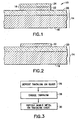
- FIG. 1 there is shown a diagram of a cross section of a subcomponent 10 incorporating features of the present invention.
- the present invention will be described with reference to the exemplary embodiment shown in the drawings, it should be understood that the present invention can be embodied in many alternate forms fitting within the scope of the appended claims. In addiction, any suitable size, shape or type of elements or materials could be used.
- the subcomponent 10 is generally intended to be used in fabricating a larger electrical component, such as a thin film ferroelectric device.
- the component 10 could be used to fabricate a ferroelectric device, such as a ferroelectric capacitor 12 (see Fig. 5 ).
- the subcomponent 10 generally comprises a substrate 14 and an electrode 16.
- the substrate 14, in the embodiment shown, is preferably a semiconductor wafer. However, in alternate embodiments, any suitable type of substrate could be provided.
- the substrate 14 generally comprises a base 18 and a top layer 20.
- the base 18 preferably comprises a 3-15 ohm-cm Phosphorous doped silicon substrate.
- any suitable type of base could be provided.
- the top layer 20 is comprised of glass.
- the glass layer 20 comprises silicon dioxide (SiO 2 ).
- the glass layer 20 could comprise 5000 ⁇ thick wet silicon oxide.
- the substrate 14 could be comprised of any suitable type of a top layer.
- the adhesion layer 22 is comprised of tantalum pentoxide (Ta 2 O 5 ).
- the electrical conductor layer 24 is comprised of a noble metal, preferably platinum.
- the noble metal conductor could be selected from a group consisting of platinum, palladium, gold and rhodium.
- the electrical conductor layer 24 is attached to the top player 20 of the substrate 14 by the adhesion layer 22.
- the adhesion issue has been dealt with by including a thin metallic adhesion layer between the platinum and the glass.
- This layer is typically composed of Ti, Cr, Ta, Va, Nb, Pd, Ir, Ru and is typically about 10% of the thickness of the platinum layer.
- Use of such adhesion layers results in very narrow process windows if the platinum electrode is to survive in oxidizing environments at temperatures above about 600°C. This is due to a combination of the tendency of platinum to plastic flow at these temperatures in response to stress and the poor performance of the platinum as a barrier to oxygen, which allows oxidation of the adhesion layer causing a volume expansion.
- the typical metallic adhesion layer is an unstable surface for the platinum in this environment.
- Ti titanium
- the most commonly used adhesion layer, titanium (Ti) has the further problem of migrating through the platinum electrodes. When used in an electrode for thin ceramic films, this causes stoiciometry changes and/or contamination issues which can result in degraded performance. Examples of this degradation include a reduction in relative permittivity for BST and reduced remnant polarization in SBTN or PZT.
- the new electrode system of the present invention combines heated deposition, to control stresses in the metal layers, and oxidation of the adhesion layer before depositing the conductive layer. Oxidation of the adhesion layer before depositing the conductive layer prevents volume expansion from occurring during subsequent thermal processing. This results in a smooth, highly adherent surface which remains smooth during subsequent processing. Further, these electrodes show little sensitivity to variations in thickness of either the platinum or the adhesion layer, little sensitivity to the purity of the deposited materials, and little sensitivity to anneal processes. This allows use of thicker electrodes which, for many applications, are required for increased power/current handling or reduced resistive loss.
- Electrodes of the present invention remain smooth and planar even when exposed to very high compressive stresses and through anneals as long as 10 hours at 725° C in oxygen. These electrodes also show higher remnant polarization (2Pr) in SBTN and lower leakage and higher breakdown fields in BST.
- Fig. 2 shows the subcomponent 10 of Fig. 1 before the electrical conductor layer 24 is formed thereon.
- Fig. 3 illustrates some of the method steps used to form the subcomponent 10.
- tantalum is deposited on the top glass layer 20.
- the tantalum is then oxidized as illustrated by block 28. This forms the assembly as shown in Fig. 2 .
- a noble metal in this embodiment Pt is deposited on the tantalum oxide as illustrated by block 30.
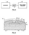
- an evaporator 32 is used for heated deposition of the tantalum and the platinum on the wafer which eventually forms the subcomponent 10.
- the tantalum and the platinum could be deposited on the wafer by any suitable method, and perhaps by different methods.
- the evaporator 32 is preferably an e-beam evaporator which can heat the wafer 15 in a vacuum.
- any suitable evaporator or metal deposition method could be used.
- the system comprises a rapid thermal processor (RTP) 34.
- RTP rapid thermal processor
- any suitable device for oxidizing the tantalum could be used, including in-situ oxidations within the metal deposition system by the introduction of oxygen, direct evaporation of TA 2 O 5 or reactive sputter of TA 2 O 5 in an O 2 environment.
- the metal oxide adhesion layer may be deposited by direct sputtering of a metal oxide target; by vacuum deposition using MOCVD of an appropriate precursor; by spin-on deposition and firing of a MOD or sol-gel precursor; or by any method suitable for depositing metal oxide films.
- the rapid thermal processor can expose the wafer 15 to an elevated temperature for a predetermined time in an oxygen ambient atmosphere. This process completely oxidizes the metallic tantalum layer.
- the wafers 15 are then placed back into the evaporator 32 and heated to a predetermined temperature in a vacuum where the noble metal (Pt in the embodiment shown) layer can be deposited.
- the predetermined temperature is about 310 degrees Celsius.
- any suitable temperature could be used.
- the platinum layer 24 has a thickness of about 2500 angstroms.
- the platinum layer could have any suitable thickness.
- the electrical conductor layer 24 could be from about 1600 angstroms to about 3500 angstroms.
- the subcomponent 10 is shown as part of a ferroelectric capacitor 12.
- the capacitor 12 generally comprises the subcomponent 10, a ferroelectric layer (FE) 42, a top electrode (TE) 44, an interlayer dielectric (ILD) 46, and an interconnect metal (M3) 48.
- the electrode 16 forms the bottom electrode for the capacitor 12.
- the electrode 16 is about 2500 ⁇ .
- the electrode could have any suitable thickness.
- the ferroelectric layer 42 is about 2000 ⁇
- the top electrode 44 is about 1100 ⁇
- the inter layer dielectric 46 is about 3000 ⁇
- the interconnect metal 48 is about 1850 ⁇ .
- the ferroelectric thin film layer 42 could comprise barium titanate, strontium titanate, barium strontium titanate, lead zirconate titanate, strontium bismuth tantalate or strontium bismuth tantalate niobate.
- the top electrode 44 is comprised of platinum.
- the top electrode 44 could comprise any suitable type of electrical conductor material.
- the interlayer dielectric 46 is comprised of low pressure chemical vapor deposition (LPCVD) SiO 2 .
- LPCVD low pressure chemical vapor deposition
- the interlayer dielectric could be comprised of any suitable type of material and formed by any suitable method.
- the interconnect metal 48 is comprised of platinum.
- the interconnect metal 48 could be comprised of any suitable type of electrical conductor material.
- the present invention can provide improved performance of thin-film dielectric and ferroelectric devices. Both leakage current and breakdown voltage of thin insulating films are dependant on the morphology of the underlying electrode. This invention allows the formation of a stable, smooth, and highly adherent electrode even with the relatively large thermal budgets required to produce high-quality ceramic thin films. Traditional films are marginal in adhesion and have a tendency to form a rough hillocked surface when exposed to high temperature oxidizing environments and high stresses.
- This new adhesive layer comprises a metal oxide, for example Ta 2 O 5 , such as formed by evaporating tantalum metal and oxidizing it in a rapid thermal processor, as a stable adhesion layer before deposition of the platinum (or other noble metal) electrode.
- a metal oxide for example Ta 2 O 5
- Ta 2 O 5 such as formed by evaporating tantalum metal and oxidizing it in a rapid thermal processor
- the electrode remains planar and very smooth over a wide range of anneal and process conditions.
- This electrode also appears to be quite insensitive to process variations such as thickness of the tantalum layer, tantalum anneal conditions, thickness of the platinum layer, and age of the platinum melt.
- Ferroelectric devices fabricated on this new electrode show improved yield, higher breakdown resistance, and improved electrical properties when compared to previous conventional electrode structures.
- Use of this electrode structure has proven important to work on a BST varactor (such as described in U.S. Patent No. 6,101,102 ) which requires very thick electrode layers to minimize resistive losses and high breakdown fields to achieve a wide tuning range and high current density.
- the substrate is a silicon wafer which has been wet oxidized to produce a 5000A thick SiO 2 film.
- the wafer is then placed in an e-beam evaporator and heated to a temperature of 250° C in a vacuum.
- a tantalum layer approximately 200A thick, is then evaporated onto the heated substrate.
- the system is vented and the wafer is allowed to cool. Neither the wafer temperature during evaporation nor the thickness of the tantalum layer are critical.
- the wafer is then removed from the system and the tantalum metal is oxidized by using a rapid thermal processor (RTP) to expose the wafer to a temperature of 725° C for two minutes in an oxygen ambient atmosphere. Again, neither the time nor the temperature of this process is critical as long as the tantalum layer is fully oxidized.
- RTP rapid thermal processor
- the wafer is then placed back into the evaporator and heated to a temperature of 310° C in a vacuum where a platinum layer about 2500A thick is deposited.
- the thickness of the platinum layer is not critical. In tests, there has been success with platinum layer ranging from 1600A to 3500A and greater with this process.
- the temperature of the wafer during this deposition might be important due to its effect on the tensile stress of the wafers after cooling. Depositions at temperatures at or above 300° C show an improvement in surface smoothness and adhesion compared to lower temperature depositions. This result in essentially featureless surfaces at magnifications up to 1000X. In a test of the process, maximum deposition temperature was limited by VITON TM seals in the vacuum system, so significantly higher temperature depositions have not been explored, but may be possible.
- the wafer After venting and cooling, the wafer is removed from the vacuum system. At this stage the wafer is reasonably adherent and smooth. If necessary, improved adhesion can be obtained by a brief exposure to a higher temperature such as 30 seconds at 725° C in an RTP, either as a separate anneal on the electrode only, or combined with the crystallization anneal on a subsequently deposited ferroelectric layer. The electrode surface will remain very smooth through the remainder of the ferroelectric processing including anneals totaling 10 hours at 725° C.
- the process can comprises the following steps:
- the process can comprise the following steps:
- the improved electrodes of the present invention can provide many benefits.
- the electrodes can provide an improved performance, such as improved switching characteristics for ferroelectrics (2Pr, 2Ec), and larger NDRO signal for ferroelectrics.
- the electrodes can comprise smoother electrode surfaces both before and after FE firing. This can provide significantly improved yield, lower leakage current, and increased breakdown.
- the improved electrode forming process can also allow thicker electrodes to be used. This can reduce conductive loss in electrodes which can dominate device performance at higher frequencies.
- the improved electrode forming process can provide larger process windows which are relatively insensitive to RTP oxidation time, Ta thickness, Pt thickness, and Pt purity.
- the present invention can provide benefits for a variety of materials such as SBTN, SBT and BST.
Landscapes
- Engineering & Computer Science (AREA)
- Power Engineering (AREA)
- Microelectronics & Electronic Packaging (AREA)
- Manufacturing & Machinery (AREA)
- General Physics & Mathematics (AREA)
- Computer Hardware Design (AREA)
- Physics & Mathematics (AREA)
- Condensed Matter Physics & Semiconductors (AREA)
- Chemical & Material Sciences (AREA)
- Materials Engineering (AREA)
- Inorganic Chemistry (AREA)
- Semiconductor Memories (AREA)
- Formation Of Insulating Films (AREA)
Abstract
Description
- The present invention relates to thin film capacitor devices or ferroelectric devices and, more particularly, to a method of forming an electrode on a glass layer of a substrate.
- Platinum (Pt) is commonly used as an electrode material for thin-film ferroelectric devices. This is due to its resistance to oxidation at temperatures above 600° C in oxygen (O2); an environment which is required to obtain good electrical characteristics from materials such as (BaSr)TiO3 (BST), (PbZr)TiO3 (PZT), SrBi2Ta2O9 (SBT), SrBi2Nb2O9 (SBN), SrBi2(TaNb)2O9 (SBTN) and others. Devices using these materials are frequently made using oxidized silicon wafers as a substrate.
- Adhesion of a platinum electrode to the oxide of the silicon wafer has always been a problem. The problem has been exacerbated due to the unique properties of platinum and challenges of thin film ferroelectric processing. Platinum has a tendency to plastic flow in response to stress at temperatures above 600° C. Ferroelectric thin film deposition is frequently performed using spin-on methods which result in a very high tensile stress due to film shrinkage as it is sintered. The ferroelectric material can contain metals such as Bi. These metals can alloy with the platinum.
- The ferroelectric processes often incorporate long anneals in O2 at elevated temperature to improve performance. Even if the platinum adheres to the substrate, these processes frequently cause the formation of hillocks or bumps on the surface of the platinum electrode. These hillocks can cause localized high electric fields, high leakage, and early breakdown. In more severe cases, hillocks can be large enough to directly short out the ferroelectric device or combine with other defects in the film to short out the devices resulting in reduced yield or unusable devices.
- Historically a thin film of titanium (Ti) has been added between the platinum and the oxide of the silicon wafer. This titanium layer is about 10% of the thickness of the platinum electrode and greatly improves adhesion of the platinum to the oxide. An example of this electrode is given in
U.S. Patent No. 5,723,171 . The use of a titanium adhesion layer has two major problems. First, the process windows are very narrow. Changes in anneal times or temperatures or changes in the thickness of the ferroelectric often require a re-optimization of the titanium and platinum layer thicknesses. Second, titanium is very mobile and can migrate through the platinum electrode causing degraded performance of the ferroelectric layer. This is a known problem with BST, SBT, SBTN and others where variations in film composition, due to titanium incorporation degrade film performance. - Other methods to improve adhesion have been employed with a wide variety of metallic layers such as Cr, Ta, Vd, Nb, Sr, Ru, Os, Pd (see
U.S. Patent Nos. 6,103,400 and6,054,311 ). While these other metals may work over some range of conditions, these processes all suffer from either poor adhesion or from volume expansion of the adhesion layer due to oxidation during high temperature oxygen anneals which results in an unstable foundation for the platinum and limits their utility. -
EP 0 785 579 discloses ferroelectric capacitors which include oxide electrodes.US 2001/0019874 discloses the use of Ti and TiO2 as a barrier to encapsulate a device, and the use of TiO2 for adhesion promotion. - The present invention provides electrodes and methods of forming electrodes as recited in the claims.
- The foregoing aspects and other features of the present invention are explained in the following description, taken in connection with the accompanying drawings, wherein:
-
Fig. 1 is a schematic, cross sectional diagram of a component incorporating features of the present invention; -
Fig. 2 is a schematic cross sectional diagram of the component shown inFig. 1 before the electrode is formed; -
Fig. 3 is a process flow chart of steps used to form the component shown inFig. 1 ; -
Fig. 4 is a diagram of some of the devices used to form the component shown inFig. 1 ; and -
Fig. 5 is a schematic cross sectional diagram of a ferroelectric capacitor incorporating features of the present invention. - Referring to
Fig. 1 , there is shown a diagram of a cross section of asubcomponent 10 incorporating features of the present invention. Although the present invention will be described with reference to the exemplary embodiment shown in the drawings, it should be understood that the present invention can be embodied in many alternate forms fitting within the scope of the appended claims. In addiction, any suitable size, shape or type of elements or materials could be used. - The
subcomponent 10 is generally intended to be used in fabricating a larger electrical component, such as a thin film ferroelectric device. For example, thecomponent 10 could be used to fabricate a ferroelectric device, such as a ferroelectric capacitor 12 (seeFig. 5 ). Thesubcomponent 10 generally comprises asubstrate 14 and anelectrode 16. - The
substrate 14, in the embodiment shown, is preferably a semiconductor wafer. However, in alternate embodiments, any suitable type of substrate could be provided. Thesubstrate 14 generally comprises abase 18 and atop layer 20. Thebase 18 preferably comprises a 3-15 ohm-cm Phosphorous doped silicon substrate. However, any suitable type of base could be provided. In the embodiment shown, thetop layer 20 is comprised of glass. In a preferred embodiment, theglass layer 20 comprises silicon dioxide (SiO2). For example, theglass layer 20 could comprise 5000 Å thick wet silicon oxide. However, in alternate embodiments, thesubstrate 14 could be comprised of any suitable type of a top layer. - The
electrode 16, in the embodiment shown, generally comprises anadhesion layer 22 and aelectrical conductor layer 24. Theadhesion layer 22 is comprised of tantalum pentoxide (Ta2O5). Theelectrical conductor layer 24 is comprised of a noble metal, preferably platinum. The noble metal conductor could be selected from a group consisting of platinum, palladium, gold and rhodium. Theelectrical conductor layer 24 is attached to thetop player 20 of thesubstrate 14 by theadhesion layer 22. - Adhesion of platinum (Pt) to glasses, such as silicon oxide (SiO2), has been a longstanding problem. Traditionally, the adhesion issue has been dealt with by including a thin metallic adhesion layer between the platinum and the glass. This layer is typically composed of Ti, Cr, Ta, Va, Nb, Pd, Ir, Ru and is typically about 10% of the thickness of the platinum layer. Use of such adhesion layers results in very narrow process windows if the platinum electrode is to survive in oxidizing environments at temperatures above about 600°C. This is due to a combination of the tendency of platinum to plastic flow at these temperatures in response to stress and the poor performance of the platinum as a barrier to oxygen, which allows oxidation of the adhesion layer causing a volume expansion. This means that the typical metallic adhesion layer is an unstable surface for the platinum in this environment.
- The most commonly used adhesion layer, titanium (Ti), has the further problem of migrating through the platinum electrodes. When used in an electrode for thin ceramic films, this causes stoiciometry changes and/or contamination issues which can result in degraded performance. Examples of this degradation include a reduction in relative permittivity for BST and reduced remnant polarization in SBTN or PZT.
- The new electrode system of the present invention combines heated deposition, to control stresses in the metal layers, and oxidation of the adhesion layer before depositing the conductive layer. Oxidation of the adhesion layer before depositing the conductive layer prevents volume expansion from occurring during subsequent thermal processing. This results in a smooth, highly adherent surface which remains smooth during subsequent processing. Further, these electrodes show little sensitivity to variations in thickness of either the platinum or the adhesion layer, little sensitivity to the purity of the deposited materials, and little sensitivity to anneal processes. This allows use of thicker electrodes which, for many applications, are required for increased power/current handling or reduced resistive loss. These electrodes of the present invention remain smooth and planar even when exposed to very high compressive stresses and through anneals as long as 10 hours at 725° C in oxygen. These electrodes also show higher remnant polarization (2Pr) in SBTN and lower leakage and higher breakdown fields in BST.
- Referring also to
Figs. 2 and 3, Fig. 2 shows thesubcomponent 10 ofFig. 1 before theelectrical conductor layer 24 is formed thereon.Fig. 3 illustrates some of the method steps used to form thesubcomponent 10. As shown byblock 26, tantalum is deposited on thetop glass layer 20. After the tantalum is deposited on thetop glass layer 20, the tantalum is then oxidized as illustrated byblock 28. This forms the assembly as shown inFig. 2 . With thetantalum oxide 22 attached to thetop glass layer 20, a noble metal (in this embodiment Pt) is deposited on the tantalum oxide as illustrated byblock 30. - Referring also to
Fig. 4 , in a preferred method, anevaporator 32 is used for heated deposition of the tantalum and the platinum on the wafer which eventually forms thesubcomponent 10. However, in alternate embodiments, the tantalum and the platinum could be deposited on the wafer by any suitable method, and perhaps by different methods. Theevaporator 32 is preferably an e-beam evaporator which can heat thewafer 15 in a vacuum. However, in alternate embodiments, any suitable evaporator or metal deposition method could be used. In order to oxidize the tantalum, the system comprises a rapid thermal processor (RTP) 34. However, in alternate embodiments, any suitable device for oxidizing the tantalum could be used, including in-situ oxidations within the metal deposition system by the introduction of oxygen, direct evaporation of TA2O5 or reactive sputter of TA2O5 in an O2 environment. The metal oxide adhesion layer may be deposited by direct sputtering of a metal oxide target; by vacuum deposition using MOCVD of an appropriate precursor; by spin-on deposition and firing of a MOD or sol-gel precursor; or by any method suitable for depositing metal oxide films. The rapid thermal processor can expose thewafer 15 to an elevated temperature for a predetermined time in an oxygen ambient atmosphere. This process completely oxidizes the metallic tantalum layer. - After the tantalum layer has been oxidized to form the
tantalum oxide layer 22, thewafers 15 are then placed back into theevaporator 32 and heated to a predetermined temperature in a vacuum where the noble metal (Pt in the embodiment shown) layer can be deposited. In a preferred embodiment, the predetermined temperature is about 310 degrees Celsius. However, in alternate embodiments, any suitable temperature could be used. In a preferred embodiment, theplatinum layer 24 has a thickness of about 2500 angstroms. However, in alternate embodiments, the platinum layer could have any suitable thickness. For example, theelectrical conductor layer 24 could be from about 1600 angstroms to about 3500 angstroms. - Referring now also to
Fig. 5 , thesubcomponent 10 is shown as part of aferroelectric capacitor 12. Thecapacitor 12 generally comprises thesubcomponent 10, a ferroelectric layer (FE) 42, a top electrode (TE) 44, an interlayer dielectric (ILD) 46, and an interconnect metal (M3) 48. In the embodiment shown, theelectrode 16 forms the bottom electrode for thecapacitor 12. In a preferred embodiment, theelectrode 16 is about 2500 Å. However, in alternate embodiments, the electrode could have any suitable thickness. - In the preferred embodiment shown, the
ferroelectric layer 42 is about 2000 Å, thetop electrode 44 is about 1100 Å, theinter layer dielectric 46 is about 3000 Å, and theinterconnect metal 48 is about 1850 Å. However, in alternate embodiments, these components could have any suitable thickness. The ferroelectricthin film layer 42 could comprise barium titanate, strontium titanate, barium strontium titanate, lead zirconate titanate, strontium bismuth tantalate or strontium bismuth tantalate niobate. In the preferred embodiment shown, thetop electrode 44 is comprised of platinum. However, in alternate embodiments, thetop electrode 44 could comprise any suitable type of electrical conductor material. In the embodiment shown, theinterlayer dielectric 46 is comprised of low pressure chemical vapor deposition (LPCVD) SiO2. However, an alternate embodiments, the interlayer dielectric could be comprised of any suitable type of material and formed by any suitable method. In the embodiment shown, theinterconnect metal 48 is comprised of platinum. However, in alternate embodiment, theinterconnect metal 48 could be comprised of any suitable type of electrical conductor material. - The present invention can provide improved performance of thin-film dielectric and ferroelectric devices. Both leakage current and breakdown voltage of thin insulating films are dependant on the morphology of the underlying electrode. This invention allows the formation of a stable, smooth, and highly adherent electrode even with the relatively large thermal budgets required to produce high-quality ceramic thin films. Traditional films are marginal in adhesion and have a tendency to form a rough hillocked surface when exposed to high temperature oxidizing environments and high stresses.
- This new adhesive layer comprises a metal oxide, for example Ta2O5, such as formed by evaporating tantalum metal and oxidizing it in a rapid thermal processor, as a stable adhesion layer before deposition of the platinum (or other noble metal) electrode. When this is combined with heated deposition of the platinum to control stresses, the electrode remains planar and very smooth over a wide range of anneal and process conditions. This electrode also appears to be quite insensitive to process variations such as thickness of the tantalum layer, tantalum anneal conditions, thickness of the platinum layer, and age of the platinum melt.
- Ferroelectric devices fabricated on this new electrode show improved yield, higher breakdown resistance, and improved electrical properties when compared to previous conventional electrode structures. Use of this electrode structure has proven important to work on a BST varactor (such as described in
U.S. Patent No. 6,101,102 ) which requires very thick electrode layers to minimize resistive losses and high breakdown fields to achieve a wide tuning range and high current density. - In a preferred embodiment the substrate is a silicon wafer which has been wet oxidized to produce a 5000A thick SiO2 film. The wafer is then placed in an e-beam evaporator and heated to a temperature of 250° C in a vacuum. A tantalum layer, approximately 200A thick, is then evaporated onto the heated substrate. The system is vented and the wafer is allowed to cool. Neither the wafer temperature during evaporation nor the thickness of the tantalum layer are critical. The wafer is then removed from the system and the tantalum metal is oxidized by using a rapid thermal processor (RTP) to expose the wafer to a temperature of 725° C for two minutes in an oxygen ambient atmosphere. Again, neither the time nor the temperature of this process is critical as long as the tantalum layer is fully oxidized.
- Good results were achieved for anneal times from 1 to 7 minutes. The anneal temperature of 725° C was chosen for convenience since 725° C is the normal anneal temperature used for ferroelectric films. Other temperatures were not explored, but certainly could be possible. While use of an RTP to perform this oxidation was initially chosen for convenience, it is likely that the use of a RTP to perform this anneal might be preferred. Long furnace tube anneals may result in a smoother Ta2O5 surface with a large grain size which platinum may not adhere to very well.
- After the tantalum layer has been oxidized, the wafer is then placed back into the evaporator and heated to a temperature of 310° C in a vacuum where a platinum layer about 2500A thick is deposited. The thickness of the platinum layer is not critical. In tests, there has been success with platinum layer ranging from 1600A to 3500A and greater with this process. The temperature of the wafer during this deposition might be important due to its effect on the tensile stress of the wafers after cooling. Depositions at temperatures at or above 300° C show an improvement in surface smoothness and adhesion compared to lower temperature depositions. This result in essentially featureless surfaces at magnifications up to 1000X. In a test of the process, maximum deposition temperature was limited by VITON™ seals in the vacuum system, so significantly higher temperature depositions have not been explored, but may be possible.
- After venting and cooling, the wafer is removed from the vacuum system. At this stage the wafer is reasonably adherent and smooth. If necessary, improved adhesion can be obtained by a brief exposure to a higher temperature such as 30 seconds at 725° C in an RTP, either as a separate anneal on the electrode only, or combined with the crystallization anneal on a subsequently deposited ferroelectric layer. The electrode surface will remain very smooth through the remainder of the ferroelectric processing including anneals totaling 10 hours at 725° C.
- These improved electrodes have been tested with several ferroelectric materials including Bi containing ferroelectric films (SBT(N)) and BST films having very high tensile stress. The devices made with the improved electrodes have improved ferroelectric performance, leakage currents, and greater current handling ability. The use of metal oxides such as Ta2O5 as an adhesion layer for platinum electrodes used with ceramic thin films is not known to exist in the prior art.
- As an overview of a capacitor array process, the process can comprises the following steps:
- Prepared starting wafer with 5000 Å wet oxidation
- Deposit Bottom Electrode (BE)
- Spin On Ferroelectric Precursor And Fire (FE)
- Deposit Top Electrode (TE)
- Etch Capacitor Stack
- Test Point 1 To Verify Good Ferroelectric Properties
- Deposit Interlayer Dielectric (ILD)
- Open Contacts (CT)
- Deposit Interconnect Metal (M3)
- Etch Interconnect Metal
-
Test Point 2 To Screen For Yield - Deposit Overglass
- Open Pads (GL)
- Final Parametric Test
- As an overview of the improved bottom electrode process of the present invention, the process can comprise the following steps:
- deposit Ta adhesion layer
- o for example, 200A evaporated into wafer at 250° C
- oxidize adhesion layer
- o for example,
RTA 2 minutes at 725° C in O2
- o for example,
- deposit Pt electrode
- o for example, 2500A evaporated onto wafers at 310° C
- if used in process without an RTP FE crystallization step, then an adhesion anneal may be desirable
- o for example,
RTA 30 seconds at 725° in O2.
- o for example,
- The improved electrodes of the present invention can provide many benefits. The electrodes can provide an improved performance, such as improved switching characteristics for ferroelectrics (2Pr, 2Ec), and larger NDRO signal for ferroelectrics. The electrodes can comprise smoother electrode surfaces both before and after FE firing. This can provide significantly improved yield, lower leakage current, and increased breakdown.
- The improved electrode forming process can also allow thicker electrodes to be used. This can reduce conductive loss in electrodes which can dominate device performance at higher frequencies. The improved electrode forming process can provide larger process windows which are relatively insensitive to RTP oxidation time, Ta thickness, Pt thickness, and Pt purity. The present invention can provide benefits for a variety of materials such as SBTN, SBT and BST.
- It should be understood that the foregoing description is only illustrative of the invention. Various alternatives and modifications can be devised by those skilled in the art without departing from the invention. Accordingly, the present invention is intended to embrace all such alternatives, modifications and variances which fall within the scope of the claims.
Claims (7)
- An electrode (16) for a thin film capacitor device (12) comprising:a tantalum pentoxide adhesion layer (22); anda noble metal conductor (24) connected on the tantalum pentoxide adhesion layer.
- An electrode as in claim 1 wherein the noble metal conductor (24) is selected from a group consisting of platinum, palladium, gold and rhodium.
- An electrode as in claim 1 wherein the noble metal conductor (24) comprises platinum.
- A method of forming an electrode (16) for a thin film capacitive device (12) comprising steps of:deposition of a tantalum pentoxide adhesion layer (22) on a top layer (20) of a glass substrate (14); anddeposition of a noble metal conductor (24) on the tantalum pentoxide adhesion layer (22).
- A method as in claim 4 wherein the metal oxide adhesion layer (22) is formed by deposition of a metal followed by oxidation.
- A method as in claim 5 wherein the step of oxidation comprises heat treatment in an oxygen containing environment.
- A method as in claim wherein the step of oxidation comprises heat treatment in a rapid thermal processor in an oxygen containing environment.
Applications Claiming Priority (3)
| Application Number | Priority Date | Filing Date | Title |
|---|---|---|---|
| US147093 | 1999-08-04 | ||
| US10/147,093 US7335552B2 (en) | 2002-05-15 | 2002-05-15 | Electrode for thin film capacitor devices |
| PCT/US2003/014934 WO2003098646A1 (en) | 2002-05-15 | 2003-05-12 | Improved electrode for thin film capacitor devices |
Publications (2)
| Publication Number | Publication Date |
|---|---|
| EP1504460A1 EP1504460A1 (en) | 2005-02-09 |
| EP1504460B1 true EP1504460B1 (en) | 2009-07-29 |
Family
ID=29418951
Family Applications (1)
| Application Number | Title | Priority Date | Filing Date |
|---|---|---|---|
| EP03734002A Expired - Lifetime EP1504460B1 (en) | 2002-05-15 | 2003-05-12 | Improved electrode for thin film capacitor devices |
Country Status (6)
| Country | Link |
|---|---|
| US (2) | US7335552B2 (en) |
| EP (1) | EP1504460B1 (en) |
| JP (1) | JP5059290B2 (en) |
| KR (1) | KR100699397B1 (en) |
| DE (1) | DE60328596D1 (en) |
| WO (1) | WO2003098646A1 (en) |
Families Citing this family (6)
| Publication number | Priority date | Publication date | Assignee | Title |
|---|---|---|---|---|
| KR100634509B1 (en) * | 2004-08-20 | 2006-10-13 | 삼성전자주식회사 | Three dimensional capacitor and method of manufacturing the same |
| US20060065916A1 (en) | 2004-09-29 | 2006-03-30 | Xubai Zhang | Varactors and methods of manufacture and use |
| KR20070101857A (en) * | 2004-12-06 | 2007-10-17 | 더 프레지던트 앤드 펠로우즈 오브 하바드 칼리지 | Nanoscale wire-based data storage |
| DE102005048774B4 (en) * | 2005-10-07 | 2009-04-02 | Fraunhofer-Gesellschaft zur Förderung der angewandten Forschung e.V. | Substrate, which is at least partially provided on a surface with a coating of a metal, and its use |
| US7560392B2 (en) * | 2006-05-10 | 2009-07-14 | Micron Technology, Inc. | Electrical components for microelectronic devices and methods of forming the same |
| KR100849187B1 (en) * | 2006-06-30 | 2008-07-30 | 주식회사 하이닉스반도체 | Method for fabricating capacitor in semiconductor device |
Family Cites Families (36)
| Publication number | Priority date | Publication date | Assignee | Title |
|---|---|---|---|---|
| US19874A (en) * | 1858-04-06 | Improvement in cotton-seed planters | ||
| DE2513858C3 (en) | 1975-03-27 | 1981-08-06 | Siemens AG, 1000 Berlin und 8000 München | Process for the production of a tantalum thin film capacitor |
| JPS5874079A (en) * | 1981-10-28 | 1983-05-04 | Japan Electronic Ind Dev Assoc<Jeida> | Thin film transistor |
| KR930012120B1 (en) * | 1991-07-03 | 1993-12-24 | 삼성전자 주식회사 | Semicondcutor device and fabricating method thereof |
| US5142438A (en) * | 1991-11-15 | 1992-08-25 | Micron Technology, Inc. | Dram cell having a stacked capacitor with a tantalum lower plate, a tantalum oxide dielectric layer, and a silicide buried contact |
| US5390072A (en) * | 1992-09-17 | 1995-02-14 | Research Foundation Of State University Of New York | Thin film capacitors |
| US5723171A (en) * | 1992-10-23 | 1998-03-03 | Symetrix Corporation | Integrated circuit electrode structure and process for fabricating same |
| US5479317A (en) * | 1994-10-05 | 1995-12-26 | Bell Communications Research, Inc. | Ferroelectric capacitor heterostructure and method of making same |
| US6204111B1 (en) * | 1994-12-28 | 2001-03-20 | Matsushita Electronics Corporation | Fabrication method of capacitor for integrated circuit |
| JP3098923B2 (en) * | 1994-12-28 | 2000-10-16 | 松下電子工業株式会社 | Semiconductor device and manufacturing method thereof |
| JP3480624B2 (en) * | 1995-06-09 | 2003-12-22 | シャープ株式会社 | Ferroelectric thin film coated substrate, method of manufacturing the same, and capacitor structure element |
| GB9512529D0 (en) * | 1995-06-20 | 1995-08-23 | Bnfl Fluorchem Ltd | Cell treatment |
| JP3929513B2 (en) * | 1995-07-07 | 2007-06-13 | ローム株式会社 | Dielectric capacitor and manufacturing method thereof |
| KR100234000B1 (en) * | 1996-09-04 | 1999-12-15 | 박호군 | Pzt thin films and fabricating method thereof |
| KR19980077149A (en) * | 1997-04-17 | 1998-11-16 | 윤종용 | Capacitor of Ferroelectric Memory with Multi-layered Electrode Structure and Manufacturing Method Thereof |
| US6054355A (en) * | 1997-06-30 | 2000-04-25 | Kabushiki Kaisha Toshiba | Method of manufacturing a semiconductor device which includes forming a dummy gate |
| JPH11195768A (en) * | 1997-10-22 | 1999-07-21 | Fujitsu Ltd | Electronic device including perovskite-type oxide film, manufacture thereof and ferroelectric capacitor |
| US6180481B1 (en) * | 1998-01-09 | 2001-01-30 | Micron Technology, Inc. | Barrier layer fabrication methods |
| JPH11205898A (en) * | 1998-01-16 | 1999-07-30 | Mitsubishi Electric Corp | Electrode for dielectric thin-film element, its manufacture and ultrasonic oscillator using the electrode |
| JP3125922B2 (en) * | 1998-01-20 | 2001-01-22 | ソニー株式会社 | Dielectric memory and method of manufacturing the same |
| JP3226166B2 (en) * | 1998-02-06 | 2001-11-05 | ソニー株式会社 | Ferroelectric capacitor, method of manufacturing the same, and ferroelectric memory |
| KR100324601B1 (en) * | 1998-12-30 | 2002-04-17 | 박종섭 | Method for forming ferroelectric capacitor capable of improving characteristics of interfaces |
| US6483691B1 (en) * | 1999-02-04 | 2002-11-19 | Rohm Co., Ltd. | Capacitor and method for manufacturing the same |
| US6101102A (en) * | 1999-04-28 | 2000-08-08 | Raytheon Company | Fixed frequency regulation circuit employing a voltage variable dielectric capacitor |
| JP2001223345A (en) * | 1999-11-30 | 2001-08-17 | Hitachi Ltd | Semiconductor device and its manufacturing method |
| US6417537B1 (en) * | 2000-01-18 | 2002-07-09 | Micron Technology, Inc. | Metal oxynitride capacitor barrier layer |
| US6682772B1 (en) * | 2000-04-24 | 2004-01-27 | Ramtron International Corporation | High temperature deposition of Pt/TiOx for bottom electrodes |
| KR100604662B1 (en) * | 2000-06-30 | 2006-07-25 | 주식회사 하이닉스반도체 | Semiconductor device capable of improving adhesion characteristic between upper electrode and interlayer insulating layer and method for forming the same |
| US6492242B1 (en) * | 2000-07-03 | 2002-12-10 | Chartered Semiconductor Manufacturing Ltd. | Method of forming of high K metallic dielectric layer |
| JP2002094018A (en) * | 2000-09-14 | 2002-03-29 | Fujitsu Ltd | Method of manufacturing electronic device |
| KR100338780B1 (en) * | 2000-09-15 | 2002-06-01 | 윤종용 | Semiconductor memory device for reducing the damage of interlevel dielectric layer, and fabrication method thereof |
| JP2002124647A (en) * | 2000-10-18 | 2002-04-26 | Sharp Corp | Semiconductor device |
| KR100506082B1 (en) * | 2000-12-18 | 2005-08-04 | 삼성전자주식회사 | Method for manufacturing ink-jet print head having semispherical ink chamber |
| JP2003031806A (en) * | 2001-05-09 | 2003-01-31 | Hitachi Ltd | Mos transistor method for manufacturing it |
| US6461914B1 (en) * | 2001-08-29 | 2002-10-08 | Motorola, Inc. | Process for making a MIM capacitor |
| JP4067079B2 (en) * | 2001-12-26 | 2008-03-26 | 松下電器産業株式会社 | Semiconductor device and manufacturing method thereof |
-
2002
- 2002-05-15 US US10/147,093 patent/US7335552B2/en not_active Expired - Lifetime
-
2003
- 2003-05-12 WO PCT/US2003/014934 patent/WO2003098646A1/en active Application Filing
- 2003-05-12 EP EP03734002A patent/EP1504460B1/en not_active Expired - Lifetime
- 2003-05-12 KR KR1020047018348A patent/KR100699397B1/en active IP Right Grant
- 2003-05-12 JP JP2004506049A patent/JP5059290B2/en not_active Expired - Fee Related
- 2003-05-12 DE DE60328596T patent/DE60328596D1/en not_active Expired - Lifetime
-
2007
- 2007-12-20 US US12/004,178 patent/US7545625B2/en not_active Expired - Lifetime
Also Published As
| Publication number | Publication date |
|---|---|
| KR20040106543A (en) | 2004-12-17 |
| US7545625B2 (en) | 2009-06-09 |
| US7335552B2 (en) | 2008-02-26 |
| EP1504460A1 (en) | 2005-02-09 |
| US20080106846A1 (en) | 2008-05-08 |
| US20030216017A1 (en) | 2003-11-20 |
| JP2005526390A (en) | 2005-09-02 |
| WO2003098646A1 (en) | 2003-11-27 |
| JP5059290B2 (en) | 2012-10-24 |
| KR100699397B1 (en) | 2007-03-27 |
| DE60328596D1 (en) | 2009-09-10 |
Similar Documents
| Publication | Publication Date | Title |
|---|---|---|
| US5811851A (en) | Pre-oxidizing high-dielectric-constant material electrodes | |
| KR100314489B1 (en) | A simple method of fabricating ferroelectric capacitors | |
| US5122923A (en) | Thin-film capacitors and process for manufacturing the same | |
| KR100371891B1 (en) | Microelectronic Structures and Methods of Forming the Same | |
| US6204111B1 (en) | Fabrication method of capacitor for integrated circuit | |
| US6498097B1 (en) | Apparatus and method of forming preferred orientation-controlled platinum film using oxygen | |
| JP3188179B2 (en) | Method of manufacturing ferroelectric thin film element and method of manufacturing ferroelectric memory element | |
| US20050098819A1 (en) | Ferroelectric capacitor | |
| JPS6349907B2 (en) | ||
| JPH10189881A (en) | Capacitor with high-temperature electrode barrier its manufacture | |
| KR100373079B1 (en) | Lead germanate ferroelectric structure with multi-layered electrode and deposition method for same | |
| JP4240542B2 (en) | Integrated circuit electrode structure and fabrication method thereof | |
| US7545625B2 (en) | Electrode for thin film capacitor devices | |
| JPH0563205A (en) | Semiconductor device | |
| JPH11238861A (en) | Thin film capacitor and manufacture thereof | |
| JP2874512B2 (en) | Thin film capacitor and method of manufacturing the same | |
| JPH11220106A (en) | Semiconductor device and its manufacture | |
| US20020022277A1 (en) | Ferroelectric memory having dielectric layer of siof and method for fabricating the dielectric layer | |
| JP3120568B2 (en) | Thin film capacitors | |
| JPH10340994A (en) | Manufacture of semiconductor device | |
| JP3514940B2 (en) | Method of forming ferroelectric thin film | |
| JP2850903B2 (en) | Thin film capacitor and method of manufacturing the same | |
| JP2001102242A (en) | High dielectric thin film capacitor and its manufaturing method | |
| JPH10335597A (en) | Semiconductor device capacity element and its manufacture | |
| JPH0897380A (en) | Dielectric capacitor and manufacture thereof |
Legal Events
| Date | Code | Title | Description |
|---|---|---|---|
| PUAI | Public reference made under article 153(3) epc to a published international application that has entered the european phase |
Free format text: ORIGINAL CODE: 0009012 |
|
| 17P | Request for examination filed |
Effective date: 20040928 |
|
| AK | Designated contracting states |
Kind code of ref document: A1 Designated state(s): AT BE BG CH CY CZ DE DK EE ES FI FR GB GR HU IE IT LI LU MC NL PT RO SE SI SK TR |
|
| RIN1 | Information on inventor provided before grant (corrected) |
Inventor name: DOUGHERTY, THOMAS, K. Inventor name: DRAB, JOHN, J. Inventor name: KEHLE, KATHLEEN, A. |
|
| RBV | Designated contracting states (corrected) |
Designated state(s): DE |
|
| 17Q | First examination report despatched |
Effective date: 20071126 |
|
| GRAP | Despatch of communication of intention to grant a patent |
Free format text: ORIGINAL CODE: EPIDOSNIGR1 |
|
| GRAS | Grant fee paid |
Free format text: ORIGINAL CODE: EPIDOSNIGR3 |
|
| GRAA | (expected) grant |
Free format text: ORIGINAL CODE: 0009210 |
|
| AK | Designated contracting states |
Kind code of ref document: B1 Designated state(s): DE |
|
| REF | Corresponds to: |
Ref document number: 60328596 Country of ref document: DE Date of ref document: 20090910 Kind code of ref document: P |
|
| PLBE | No opposition filed within time limit |
Free format text: ORIGINAL CODE: 0009261 |
|
| STAA | Information on the status of an ep patent application or granted ep patent |
Free format text: STATUS: NO OPPOSITION FILED WITHIN TIME LIMIT |
|
| 26N | No opposition filed |
Effective date: 20100503 |
|
| PGFP | Annual fee paid to national office [announced via postgrant information from national office to epo] |
Ref country code: DE Payment date: 20220420 Year of fee payment: 20 |
|
| REG | Reference to a national code |
Ref country code: DE Ref legal event code: R071 Ref document number: 60328596 Country of ref document: DE |