EP1499010A2 - Frequenzumsetzer und Verfahren dazu - Google Patents
Frequenzumsetzer und Verfahren dazu Download PDFInfo
- Publication number
- EP1499010A2 EP1499010A2 EP04016453A EP04016453A EP1499010A2 EP 1499010 A2 EP1499010 A2 EP 1499010A2 EP 04016453 A EP04016453 A EP 04016453A EP 04016453 A EP04016453 A EP 04016453A EP 1499010 A2 EP1499010 A2 EP 1499010A2
- Authority
- EP
- European Patent Office
- Prior art keywords
- mhz
- signal
- signals
- phase
- ssb
- Prior art date
- Legal status (The legal status is an assumption and is not a legal conclusion. Google has not performed a legal analysis and makes no representation as to the accuracy of the status listed.)
- Granted
Links
- 238000000034 method Methods 0.000 title claims abstract description 19
- 239000000969 carrier Substances 0.000 claims abstract description 18
- 230000010363 phase shift Effects 0.000 claims abstract description 16
- 230000005540 biological transmission Effects 0.000 description 6
- 238000004891 communication Methods 0.000 description 5
- 238000010586 diagram Methods 0.000 description 5
- 238000010295 mobile communication Methods 0.000 description 3
- 230000008901 benefit Effects 0.000 description 2
- 230000002708 enhancing effect Effects 0.000 description 2
- 238000012986 modification Methods 0.000 description 2
- 230000004048 modification Effects 0.000 description 2
Images

Classifications
-
- H—ELECTRICITY
- H03—ELECTRONIC CIRCUITRY
- H03C—MODULATION
- H03C1/00—Amplitude modulation
- H03C1/52—Modulators in which carrier or one sideband is wholly or partially suppressed
- H03C1/60—Modulators in which carrier or one sideband is wholly or partially suppressed with one sideband wholly or partially suppressed
Definitions
- Systems, apparatuses, and methods consistent with the present invention generally relate to a communication system using a wide band, and more specifically, to an apparatus and a method for generating a radio signal used in a wide-band communication.
- a communication system transmits data to a reception side using a carrier frequency, which requires the generation of the carrier frequency.
- a local oscillator (LO) is utilized to generate a frequency for data transmission.
- the data is transmitted using a signal generated by the LO, or, a predetermined procedure is firstly performed when the signal generated by the LO is not a desired signal.
- the desired signal is generated by performing the predetermined procedure with respect to the signal generated by the LO using a specific signal.
- a LO signal denotes the signal generated by the LO.
- a mixer mixes the LO signal and intermediate frequency (IF) signals having a phase difference of 90° with respect to the LO signal so as to generate two signals having 90° phase difference at the same time.
- IF intermediate frequency
- a single mixer mixes the LO signal and the IF signal to simultaneously output two signals. Specifically, based on the frequency of the LO signal, one signal having a frequency higher than that of the IF signal and the other signal having a frequency lower than that of the IF signal are output A filter is used to select one of the two output signals. An undesired frequency is removed generally using a band-pass filter to pass only the desired frequency.
- SSB single sideband
- the signal By Fourier-transforming and frequency-analyzing a signal of which amplitude is modulated, the signal is shifted to frequencies above and below the carrier frequency (IF), to thus generate an upper sideband (USB) and a lower sideband (LSB) carrying the same information.
- a double sideband (DSB) transmission transmits both of the USB and the LSB, and the SSB transmission transmits only one sideband by removing unnecessary sidebands. Since audio or music does not have signal components in low frequency band, the SSB transmission alone is enough to communicate. Since the signal is transmitted to the reception side in one of the USE and the LSB, the scale of the reception side is reduced and the power consumption is lowered.
- FIG. 1 illustrates a conventional SSB generator, which is described below.
- the SSB generator includes two mixers 102 and 106 and an operator 108.
- the respective mixers 102 and 106 mix the input IF signal and LO signal.
- the mixed signals are furnished to the operator 108.
- the operator 108 performs an addition operation or a subtraction operation on the signals.
- the SSB generator outputs only one signal based on the following Equations.
- the IF signal input to the mixer 102 be cos( w IF t ) and let the LO signal be cos( w LO t ).
- the mixer 102 outputs cos( w IF t )cos( w LO t ) by mixing the received signals based on Equation 1.
- Let the IF signal input to the mixer 106 be sin( w IF t ) and let the LO signal be sin( w LO t ) .
- the mixer 106 outputs sin( w IF t ) sin( w LO t ) by mixing the received signals based on Equation 2.
- Equation 1 represents the operations of the mixer 102
- Equation 2 represents the operations of the mixer 106.
- Equation 3 the operator 108 generates the LSB signal.
- the IF signal input to the mixer 102 be sin ( w IF t ) and let the LO signal be cos( w LO t ).
- the mixer 102 outputs sin( w IF t )cos( w LO t ) by mixing the received signals based on Equation 4.
- Let the IF signal input to the mixer 106 be cos( w IF t ) and let the LO signal be sin( w LO t ).
- the mixer 106 outputs cos( w IF t ) sin ( w LO t ) by mixing the received signals based on Equation 5.
- Equation 4 represents the operations of the mixer 102
- Equation 5 represents the operations of the mixer 106.
- Equation 6 The operator 108 performs the addition operation with respect to the signal received from the mixers 102 and 106.
- Equation 6 the operator 108 generates the USB signal.
- FIG. 2 illustrates a frequency generator in the communication system which transmits data using the plurality of carriers.
- one LO signal and a plurality of the IF signals are combined to generate the desired number of carriers.
- the number of the IF signals is n-ary.
- the LO signal generated by the LO is provided to the SSB generator 202.
- the switch 200 receives the n-ary IF signals, selects one of the n-ary IF signals, and provides the selected signal to the SSB generator 202.
- the SSB generator 202 performs the same operations as in FIG. 1, to thus output a single signal.
- the signal provided to the SSB generator 202 is not preset, but is selected from the n-ary signals.
- the SSB generator 202 performs the phase shift on the received signals by a certain unit. Referring back to FIG.1, the SSB generator 202 shifts the phase of the received signal to 90°. If the number of the received signals is plural, it is hard to perform the phase shift on each signal.
- the SSB generator performs accurately the phase shift on one signal. Accordingly, upon receiving other signals, the SSB generator cannot accurately perform the phase shift. If the SSB generator is constructed to shin the phase with respect to f 1 alone, it is infeasible to accurately shift the phase with respect to input f n . The inaccurate phase shift results in error components in the signal output from the SSB generator.
- an exemplary aspect of the present invention is to provide an apparatus and a method capable of performing an accurate phase shift with respect to an entire signal received from a SSB generator.
- Another exemplary aspect of the present invention is to provide an apparatus and a method capable of enhancing data transmission by performing an accurate phase shift with respect to an entire signal received from a SSB.generator.
- a method for generating an intermediate frequency (IF) to be transferred to a single sideband (SSB) generator which generates carriers using one local oscillator (LO) signal and at least two IF signals that are received includes generating a group signal including a non-phase-shifted signal and a phase-shifted signal comprising a phase shift of a predetermined value with respect to each IF, and selecting one of at least two group signals and transferring the selected group signal to the SSB generator.
- LO local oscillator
- An apparatus for generating an intermediate frequency (IF) to be transferred to a single sideband (SSB) generator which generates carriers using one local oscillator (LO) signal and at least two IF signals that are received includes at least two phase shifters generating a group signal including a non-phase-shifted signal and a phase-shifted signal comprising a phase shift of a predetermined value with respect to each IF, and a multiplexer selecting one of at least two group signals and transferring the selected group signal to the SSB generator.
- LO local oscillator
- FIG. 1 is a diagram illustrating a conventional SSB modulation
- FIG. 2 is a diagram illustrating the generation of the SSB in a mobile communication system using a plurality of carriers
- FIG. 3 is a diagram illustrating a mobile communication system using a plurality of carriers according to an embodiment of the present invention
- FIG. 4 is a diagram illustrating the mobile communication system using the plurality of carriers according to another embodiment of the present invention.
- FIG. 5 is a diagram illustrating the multiplexer and the inverter according to an embodiment of the present invention.
- FIG. 6 is a flowchart illustrating exemplary operations of the multiplexer and the inverter according to an embodiment of the present invention.
- a method according to an embodiment of the present invention transfers an intermediate frequency (IF) signal, whose phase is shifted, to a single sideband (SSB) generator, which is described in great detail below.
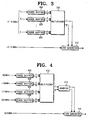
- FIG. 3 illustrates a frequency generator which generates a plurality of carriers according to an embodiment of the present invention.
- the frequency generator includes a plurality of phase shifters 300 to 304, a multiplexer 310, and a SSB generator 312.
- the phase shifters 300, 302 and 304 simultaneously output a phase-shifted signal and a non-phase-shifted signal.
- the signals transferred from each of the phase shifters 300 to 304 are referred to as a group signal.
- the group signals generated in the phase shifters 300, 302 and 304 are transferred to the multiplexer 310.
- the multiplexer 310 transfers to the SSB generator 312 desired signals among the received signals.
- the signals transferred from the multiplexer 310 are a phase-shifted signal and a non-phase-shined signal with respect to one signal.
- a switch as the multiplexer 310, may be utilized to select the signal to be transferred to the SSB generator 312.
- the SSB generator 312 generates a single signal using the signals received from the multiplexer 310 and a local oscillator (LO) signal, and outputs the generated signal.
- the SSB generator 312 performs the phase shift only on the LO signal and not on the signals transferred form the multiplexer 310, thus enhancing the efficiency of the SSB generator 312.
- signals (carriers) to be generated in the SSB generator 312 are at frequencies of about 3432 MHz, 3960 MHz, 4488 MHz, 6336 MHz, 6864 MHz, 7392 MHz, and 7920 MHz.
- the LO signal is at a frequency of about 5676 MHz
- the IF signals are combinations of frequencies of about 528 MHz and 660 MHz.
- the SSB generator 312 can generate signals using the LO signal and the IF signals as shown in Table 1.
- FIG. 4 illustrates the frequency generator using the plurality of carriers according to another embodiment of the present invention.
- signals transferred to the phase shiners 400, 402, 404 and 406 are frequencies of about 660 MHz, 1188 MHz, 1716 MHz, and 2244 MHz, respectively. These signals can be generated by combining the frequency signals of about 660 MHz and 528 MHz of Table 1. That is, the frequency signal of about 1188 MHz is generated by combining frequency signals of about 660 MHz and 528 MHz, and the frequency signal of about 2244 MHz is generated by combining fiequency signals of about 660 MHz and 3 ⁇ 528 MHz.
- Each phase shifter 400, 402, 404 and 406 generates a phase-shifted signal and a non-phase-shifted signal with respect to the received signal, and transfers the generated signals to the multiplexer 410.
- the multiplexer 410 selects desired signals among the received signals and transfers the selected signals to an inverter 412.
- the signals selected by the multiplexer 410 are a phase-shifted signal and a non-phase-shifted signal with respect to one signal.
- the inverter 412 determines whether to invert the received signals. If so, the inverter 412 inverts the received signals and transfers the inverted signals to the SSB generator 414. If not, the inverter 412 transfers the received signals to the SSB generator 414. Since the signals are passed through the multiplexer 410 and the inverter 412, the number of the signals to be input to the SSB generator 414 is eight One signal includes the phase-shifted signal and the non-phase-shifted signal.
- the signals to be input to the SSB generator 414 are at frequencies of about -660 MHz, -1188 MHz, -1716 MHz, -2244 MHz, 660 MHz, 1188 MHz, 1716 MHz, and 2244 MHz.
- the SSB generator 414 generates and outputs a single signal using a frequency of about 5676 MHz and the signals received from the inverter 412. As mentioned above, the SSB generator 414 performs the phase shift only on the signal at a frequency of about 5676 MHz and not on the signals received from the inverter 412.
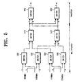
- FIG. 5 illustrates structures of the multiplexer 410 and the inverter 412, which are described in detail below.
- the phase-shifted signal be an I signal and the non-phase-shifted signal be a Q signal.
- the I signal of about 660 MHz output from the phase shifter 400 is transferred to the switch 500, and the Q signal of about 660 MHz is transferred to the switch 502.
- the I signal of about 1188 MHz output from the phase shifter 402 is transferred to the switch 500, and the Q signal of about 1188 MHz is transferred to the switch 502.
- the I signal of about 1716 MHz output from the phase shifter 404 is transferred to the switch 504, and the Q signal of about 1716 MHz is transferred to the switch 506.
- the I signal of about 2244 MHz output from the phase shifter 406 is transferred to the switch 504, and the Q signal of about 2244 MHz is transferred to the switch 506.
- the switches 500 to 506 select signals to be transferred to the SSB generator 414 and transfer the selected signals to the switches 510 and 512. Specifically, one signal is selected from the two signals inputted into the switch 500, the other signal is selected from the two signals inputted into the switch 504, and the two selected signals are transferred to the switch 510. One signal is selected from the two signals inputted into the switch 502, the other signal is selected from the two signals inputted into the switch 506, and the two selected signals are transferred to the switch 512.
- the switch 510 receives only one signal to be transferred to the SSB generator 414 at a certain time, but may receive two signals including the signal to be transferred.
- the switch 512 receives the signals having the same frequencies as the signals which are transferred to the switch 510.
- the switch 510 outputs a signal to be transferred to the SSB generator 414 among the received signals.
- the switch 512 also outputs a signal to be transferred to the SSB generator 414 among the received signals.
- the output signal of the switch 510 is transferred to the switch 520 or the switch 522, and that of the switch 512 is transferred to the switch 520 or the switch 522.
- the switch 520 or the switch 522 determines whether to invert the received signal. If not, the switch 520 outputs the I signal among the received signals, and the switch 522 outputs the Q signal among the received signals. If the received signals are inverted, the switch 520 outputs the Q signal among the received signal, and the switch 522 outputs the I signal among the received signals.
- the output signals of the switches 520 and 522 are transferred to the SSB generator 414.
- the output signal of the switch 520 is mixed with the I signal of about 5676 MHz in the SSB generator 414, and that of the switch 522 is mixed with the Q signal of about 5676 MHz in the SSB generator 414.
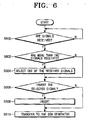
- FIG. 6 illustrates exemplary operations of the multiplexer and the inverter according to an embodiment of the present invention, which are described in detail below.
- the multiplexer determines whether the signals are received at step S600. If not, the multiplexer performs the step S600. If so, the multiplexer determines whether the number of the received signals is equal to or more than two at step S602. If more than two signals are received, the multiplexer selects one of the received signals at step S604. If not, that is, if one signal is received, the inverter determines whether to invert the received signal at step S606.
- the inverter inverts the selected signal at step S608 and transfers the inverted signal to the SSB generator at step S610. If not, the inverter transfers the non-inverted signal to the SSB generator. Accordingly, the phase-shifted signal and the non-phase-shifted signal are generated from the single signal.
- the phase-shifted signal is transferred to the SSB generator according to an embodiment of the present invention.
- the SSB generator which is available in the wide band by combining the narrow-band devices.
- the phase shifting is efficiently performed without having to use the phase shifter for the wide band signals.
Landscapes
- Superheterodyne Receivers (AREA)
- Transmitters (AREA)
- Transceivers (AREA)
- Digital Transmission Methods That Use Modulated Carrier Waves (AREA)
Applications Claiming Priority (4)
| Application Number | Priority Date | Filing Date | Title |
|---|---|---|---|
| US48641603P | 2003-07-14 | 2003-07-14 | |
| US486416P | 2003-07-14 | ||
| KR2004021466 | 2004-03-30 | ||
| KR1020040021466A KR100565787B1 (ko) | 2003-07-14 | 2004-03-30 | 초광대역 통신 시스템에서 주파수 생성 장치 및 방법 |
Publications (3)
| Publication Number | Publication Date |
|---|---|
| EP1499010A2 true EP1499010A2 (de) | 2005-01-19 |
| EP1499010A3 EP1499010A3 (de) | 2005-07-20 |
| EP1499010B1 EP1499010B1 (de) | 2013-09-25 |
Family
ID=33479061
Family Applications (1)
| Application Number | Title | Priority Date | Filing Date |
|---|---|---|---|
| EP20040016453 Active EP1499010B1 (de) | 2003-07-14 | 2004-07-13 | Frequenzumsetzer und Verfahren dazu |
Country Status (3)
| Country | Link |
|---|---|
| EP (1) | EP1499010B1 (de) |
| JP (1) | JP3962398B2 (de) |
| CN (1) | CN100531169C (de) |
Families Citing this family (2)
| Publication number | Priority date | Publication date | Assignee | Title |
|---|---|---|---|---|
| JP4646856B2 (ja) | 2006-06-09 | 2011-03-09 | ルネサスエレクトロニクス株式会社 | 周波数シンセサイザ |
| KR101721391B1 (ko) * | 2009-03-17 | 2017-03-29 | 스카이워크스 솔루션즈, 인코포레이티드 | Saw 없고, lna 없는 저잡음 수신기 |
Citations (3)
| Publication number | Priority date | Publication date | Assignee | Title |
|---|---|---|---|---|
| US4955083A (en) * | 1986-10-31 | 1990-09-04 | Motorola, Inc. | Dual mode radio transceiver for an SSB communication system |
| EP0801465A1 (de) * | 1996-04-12 | 1997-10-15 | Continental Electronics Corporation | Funksendegerät |
| US6519279B1 (en) * | 2000-01-05 | 2003-02-11 | Motorola, Inc. | Transceiver circuitry, portable communication device and method for performing radio communication |
-
2004
- 2004-07-13 EP EP20040016453 patent/EP1499010B1/de active Active
- 2004-07-14 JP JP2004207117A patent/JP3962398B2/ja active Active
- 2004-07-14 CN CNB200410079438XA patent/CN100531169C/zh active Active
Patent Citations (3)
| Publication number | Priority date | Publication date | Assignee | Title |
|---|---|---|---|---|
| US4955083A (en) * | 1986-10-31 | 1990-09-04 | Motorola, Inc. | Dual mode radio transceiver for an SSB communication system |
| EP0801465A1 (de) * | 1996-04-12 | 1997-10-15 | Continental Electronics Corporation | Funksendegerät |
| US6519279B1 (en) * | 2000-01-05 | 2003-02-11 | Motorola, Inc. | Transceiver circuitry, portable communication device and method for performing radio communication |
Also Published As
| Publication number | Publication date |
|---|---|
| EP1499010B1 (de) | 2013-09-25 |
| CN100531169C (zh) | 2009-08-19 |
| CN1592286A (zh) | 2005-03-09 |
| EP1499010A3 (de) | 2005-07-20 |
| JP3962398B2 (ja) | 2007-08-22 |
| JP2005039827A (ja) | 2005-02-10 |
Similar Documents
| Publication | Publication Date | Title |
|---|---|---|
| JP7043486B2 (ja) | 集積回路におけるシングルバンド送信および受信径路からマルチバンド送信および受信径路への再構成 | |
| US7345551B2 (en) | Frequency synthesizer for mixing reference frequencies | |
| US8502615B2 (en) | Jumpless phase modulation in a polar modulation environment | |
| US20070149143A1 (en) | Local oscillation frequency generation apparatus and wireless transceiver having the same | |
| JPS5819038A (ja) | 周波数偏移変調信号用無線受信装置 | |
| JPH0382248A (ja) | 90度移相器とデータ受信機 | |
| EP0807344B1 (de) | Verfahren und anordnung zum erzeugen von mehreren quadraturmodulierten trägern | |
| US7804911B2 (en) | Dual demodulation mode AM radio | |
| US6747524B2 (en) | Modulator and demodulator | |
| US7218898B2 (en) | Apparatus and method for frequency generation in mobile communication system | |
| JP2005287065A (ja) | ミリ波帯通信装置 | |
| EP1499030A2 (de) | Breitbandige Quadraturerzeugungstechnik, welche nur schmalbandige Komponenten erfordert und Verfahren dazu | |
| EP1499010A2 (de) | Frequenzumsetzer und Verfahren dazu | |
| JPH11340860A (ja) | マルチバンド移動無線機 | |
| JP2004356927A (ja) | 無線通信装置 | |
| KR100565786B1 (ko) | 협대역 장치만을 이용한 광대역 직교 변조 신호 발생 장치및 방법 | |
| JP2006352623A (ja) | 送信装置,受信装置,送受信システム及び送受信方法 | |
| CN102882822B (zh) | 信号调制器与信号调制方法 | |
| JP3056172B2 (ja) | 携帯電話装置 | |
| JPH0774790A (ja) | 非線形歪補償送受信回路 | |
| KR920000167B1 (ko) | 등가포락선을 가진 이중위상변조회로 | |
| US8891680B2 (en) | Transmission arrangement and method for modulating useful signals onto a carrier frequency signal | |
| JP4231012B2 (ja) | Mimo受信機及びmimo送信機 | |
| JP2022098081A (ja) | 無線通信装置及び無線通信方法 | |
| CN116996099A (zh) | 蓝牙发射器、蓝牙装置与发射器 |
Legal Events
| Date | Code | Title | Description |
|---|---|---|---|
| PUAI | Public reference made under article 153(3) epc to a published international application that has entered the european phase |
Free format text: ORIGINAL CODE: 0009012 |
|
| 17P | Request for examination filed |
Effective date: 20040713 |
|
| AK | Designated contracting states |
Kind code of ref document: A2 Designated state(s): AT BE BG CH CY CZ DE DK EE ES FI FR GB GR HU IE IT LI LU MC NL PL PT RO SE SI SK TR |
|
| AX | Request for extension of the european patent |
Extension state: AL HR LT LV MK |
|
| PUAL | Search report despatched |
Free format text: ORIGINAL CODE: 0009013 |
|
| AK | Designated contracting states |
Kind code of ref document: A3 Designated state(s): AT BE BG CH CY CZ DE DK EE ES FI FR GB GR HU IE IT LI LU MC NL PL PT RO SE SI SK TR |
|
| AX | Request for extension of the european patent |
Extension state: AL HR LT LV MK |
|
| AKX | Designation fees paid |
Designated state(s): DE FR GB NL |
|
| RAP1 | Party data changed (applicant data changed or rights of an application transferred) |
Owner name: SAMSUNG ELECTRONICS CO., LTD. Owner name: STACCATO COMMUNICATIONS, INC. |
|
| RAP1 | Party data changed (applicant data changed or rights of an application transferred) |
Owner name: STACCATO COMMUNICATIONS, INC. Owner name: SAMSUNG ELECTRONICS CO., LTD. |
|
| GRAP | Despatch of communication of intention to grant a patent |
Free format text: ORIGINAL CODE: EPIDOSNIGR1 |
|
| INTG | Intention to grant announced |
Effective date: 20130405 |
|
| GRAS | Grant fee paid |
Free format text: ORIGINAL CODE: EPIDOSNIGR3 |
|
| GRAA | (expected) grant |
Free format text: ORIGINAL CODE: 0009210 |
|
| AK | Designated contracting states |
Kind code of ref document: B1 Designated state(s): DE FR GB NL |
|
| REG | Reference to a national code |
Ref country code: GB Ref legal event code: FG4D |
|
| REG | Reference to a national code |
Ref country code: DE Ref legal event code: R096 Ref document number: 602004043400 Country of ref document: DE Effective date: 20131121 |
|
| REG | Reference to a national code |
Ref country code: NL Ref legal event code: VDEP Effective date: 20130925 |
|
| PG25 | Lapsed in a contracting state [announced via postgrant information from national office to epo] |
Ref country code: NL Free format text: LAPSE BECAUSE OF FAILURE TO SUBMIT A TRANSLATION OF THE DESCRIPTION OR TO PAY THE FEE WITHIN THE PRESCRIBED TIME-LIMIT Effective date: 20130925 |
|
| REG | Reference to a national code |
Ref country code: DE Ref legal event code: R097 Ref document number: 602004043400 Country of ref document: DE |
|
| PLBE | No opposition filed within time limit |
Free format text: ORIGINAL CODE: 0009261 |
|
| STAA | Information on the status of an ep patent application or granted ep patent |
Free format text: STATUS: NO OPPOSITION FILED WITHIN TIME LIMIT |
|
| 26N | No opposition filed |
Effective date: 20140626 |
|
| REG | Reference to a national code |
Ref country code: DE Ref legal event code: R097 Ref document number: 602004043400 Country of ref document: DE Effective date: 20140626 |
|
| GBPC | Gb: european patent ceased through non-payment of renewal fee |
Effective date: 20140713 |
|
| REG | Reference to a national code |
Ref country code: FR Ref legal event code: ST Effective date: 20150331 |
|
| PG25 | Lapsed in a contracting state [announced via postgrant information from national office to epo] |
Ref country code: FR Free format text: LAPSE BECAUSE OF NON-PAYMENT OF DUE FEES Effective date: 20140731 Ref country code: GB Free format text: LAPSE BECAUSE OF NON-PAYMENT OF DUE FEES Effective date: 20140713 |
|
| PGFP | Annual fee paid to national office [announced via postgrant information from national office to epo] |
Ref country code: DE Payment date: 20230524 Year of fee payment: 20 |