EP1498959A2 - Manufacturing method of a semiconductor device - Google Patents
Manufacturing method of a semiconductor device Download PDFInfo
- Publication number
- EP1498959A2 EP1498959A2 EP04253509A EP04253509A EP1498959A2 EP 1498959 A2 EP1498959 A2 EP 1498959A2 EP 04253509 A EP04253509 A EP 04253509A EP 04253509 A EP04253509 A EP 04253509A EP 1498959 A2 EP1498959 A2 EP 1498959A2
- Authority
- EP
- European Patent Office
- Prior art keywords
- substrate
- adhesive
- manufacturing
- holder
- sealing member
- Prior art date
- Legal status (The legal status is an assumption and is not a legal conclusion. Google has not performed a legal analysis and makes no representation as to the accuracy of the status listed.)
- Withdrawn
Links
Images


Classifications
-
- H—ELECTRICITY
- H10—SEMICONDUCTOR DEVICES; ELECTRIC SOLID-STATE DEVICES NOT OTHERWISE PROVIDED FOR
- H10F—INORGANIC SEMICONDUCTOR DEVICES SENSITIVE TO INFRARED RADIATION, LIGHT, ELECTROMAGNETIC RADIATION OF SHORTER WAVELENGTH OR CORPUSCULAR RADIATION
- H10F39/00—Integrated devices, or assemblies of multiple devices, comprising at least one element covered by group H10F30/00, e.g. radiation detectors comprising photodiode arrays
- H10F39/10—Integrated devices
- H10F39/12—Image sensors
-
- H—ELECTRICITY
- H10—SEMICONDUCTOR DEVICES; ELECTRIC SOLID-STATE DEVICES NOT OTHERWISE PROVIDED FOR
- H10F—INORGANIC SEMICONDUCTOR DEVICES SENSITIVE TO INFRARED RADIATION, LIGHT, ELECTROMAGNETIC RADIATION OF SHORTER WAVELENGTH OR CORPUSCULAR RADIATION
- H10F39/00—Integrated devices, or assemblies of multiple devices, comprising at least one element covered by group H10F30/00, e.g. radiation detectors comprising photodiode arrays
- H10F39/80—Constructional details of image sensors
- H10F39/804—Containers or encapsulations
-
- H—ELECTRICITY
- H04—ELECTRIC COMMUNICATION TECHNIQUE
- H04N—PICTORIAL COMMUNICATION, e.g. TELEVISION
- H04N23/00—Cameras or camera modules comprising electronic image sensors; Control thereof
- H04N23/57—Mechanical or electrical details of cameras or camera modules specially adapted for being embedded in other devices
-
- H—ELECTRICITY
- H10—SEMICONDUCTOR DEVICES; ELECTRIC SOLID-STATE DEVICES NOT OTHERWISE PROVIDED FOR
- H10F—INORGANIC SEMICONDUCTOR DEVICES SENSITIVE TO INFRARED RADIATION, LIGHT, ELECTROMAGNETIC RADIATION OF SHORTER WAVELENGTH OR CORPUSCULAR RADIATION
- H10F39/00—Integrated devices, or assemblies of multiple devices, comprising at least one element covered by group H10F30/00, e.g. radiation detectors comprising photodiode arrays
- H10F39/011—Manufacture or treatment of image sensors covered by group H10F39/12
-
- H—ELECTRICITY
- H10—SEMICONDUCTOR DEVICES; ELECTRIC SOLID-STATE DEVICES NOT OTHERWISE PROVIDED FOR
- H10F—INORGANIC SEMICONDUCTOR DEVICES SENSITIVE TO INFRARED RADIATION, LIGHT, ELECTROMAGNETIC RADIATION OF SHORTER WAVELENGTH OR CORPUSCULAR RADIATION
- H10F39/00—Integrated devices, or assemblies of multiple devices, comprising at least one element covered by group H10F30/00, e.g. radiation detectors comprising photodiode arrays
- H10F39/011—Manufacture or treatment of image sensors covered by group H10F39/12
- H10F39/024—Manufacture or treatment of image sensors covered by group H10F39/12 of coatings or optical elements
-
- H—ELECTRICITY
- H10—SEMICONDUCTOR DEVICES; ELECTRIC SOLID-STATE DEVICES NOT OTHERWISE PROVIDED FOR
- H10F—INORGANIC SEMICONDUCTOR DEVICES SENSITIVE TO INFRARED RADIATION, LIGHT, ELECTROMAGNETIC RADIATION OF SHORTER WAVELENGTH OR CORPUSCULAR RADIATION
- H10F39/00—Integrated devices, or assemblies of multiple devices, comprising at least one element covered by group H10F30/00, e.g. radiation detectors comprising photodiode arrays
- H10F39/80—Constructional details of image sensors
- H10F39/806—Optical elements or arrangements associated with the image sensors
-
- H—ELECTRICITY
- H10—SEMICONDUCTOR DEVICES; ELECTRIC SOLID-STATE DEVICES NOT OTHERWISE PROVIDED FOR
- H10W—GENERIC PACKAGES, INTERCONNECTIONS, CONNECTORS OR OTHER CONSTRUCTIONAL DETAILS OF DEVICES COVERED BY CLASS H10
- H10W99/00—Subject matter not provided for in other groups of this subclass
-
- H—ELECTRICITY
- H10—SEMICONDUCTOR DEVICES; ELECTRIC SOLID-STATE DEVICES NOT OTHERWISE PROVIDED FOR
- H10F—INORGANIC SEMICONDUCTOR DEVICES SENSITIVE TO INFRARED RADIATION, LIGHT, ELECTROMAGNETIC RADIATION OF SHORTER WAVELENGTH OR CORPUSCULAR RADIATION
- H10F77/00—Constructional details of devices covered by this subclass
- H10F77/40—Optical elements or arrangements
-
- H—ELECTRICITY
- H10—SEMICONDUCTOR DEVICES; ELECTRIC SOLID-STATE DEVICES NOT OTHERWISE PROVIDED FOR
- H10F—INORGANIC SEMICONDUCTOR DEVICES SENSITIVE TO INFRARED RADIATION, LIGHT, ELECTROMAGNETIC RADIATION OF SHORTER WAVELENGTH OR CORPUSCULAR RADIATION
- H10F77/00—Constructional details of devices covered by this subclass
- H10F77/50—Encapsulations or containers
-
- H—ELECTRICITY
- H10—SEMICONDUCTOR DEVICES; ELECTRIC SOLID-STATE DEVICES NOT OTHERWISE PROVIDED FOR
- H10W—GENERIC PACKAGES, INTERCONNECTIONS, CONNECTORS OR OTHER CONSTRUCTIONAL DETAILS OF DEVICES COVERED BY CLASS H10
- H10W72/00—Interconnections or connectors in packages
- H10W72/50—Bond wires
- H10W72/551—Materials of bond wires
- H10W72/552—Materials of bond wires comprising metals or metalloids, e.g. silver
- H10W72/5522—Materials of bond wires comprising metals or metalloids, e.g. silver comprising gold [Au]
-
- H—ELECTRICITY
- H10—SEMICONDUCTOR DEVICES; ELECTRIC SOLID-STATE DEVICES NOT OTHERWISE PROVIDED FOR
- H10W—GENERIC PACKAGES, INTERCONNECTIONS, CONNECTORS OR OTHER CONSTRUCTIONAL DETAILS OF DEVICES COVERED BY CLASS H10
- H10W90/00—Package configurations
- H10W90/701—Package configurations characterised by the relative positions of pads or connectors relative to package parts
- H10W90/751—Package configurations characterised by the relative positions of pads or connectors relative to package parts of bond wires
- H10W90/752—Package configurations characterised by the relative positions of pads or connectors relative to package parts of bond wires between stacked chips
-
- H—ELECTRICITY
- H10—SEMICONDUCTOR DEVICES; ELECTRIC SOLID-STATE DEVICES NOT OTHERWISE PROVIDED FOR
- H10W—GENERIC PACKAGES, INTERCONNECTIONS, CONNECTORS OR OTHER CONSTRUCTIONAL DETAILS OF DEVICES COVERED BY CLASS H10
- H10W90/00—Package configurations
- H10W90/701—Package configurations characterised by the relative positions of pads or connectors relative to package parts
- H10W90/751—Package configurations characterised by the relative positions of pads or connectors relative to package parts of bond wires
- H10W90/754—Package configurations characterised by the relative positions of pads or connectors relative to package parts of bond wires between a chip and a stacked insulating package substrate, interposer or RDL
Definitions
- the present invention generally relates to manufacturing methods of semiconductor devices, and more particularly, to a manufacturing method of a semiconductor device that includes a step of sealing the semiconductor device by providing a sealing member on a substrate mounting a semiconductor element thereon.
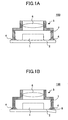
- FIG. 1A shows such a conventional imaging apparatus 100.
- the imaging apparatus 100 generally includes an optical sensor element 1, a substrate 2, and a holder 5.
- the optical sensor element 1 is, for example, a CCD image sensor or a CMOS image sensor.
- the optical sensor element 1 is mounted on the substrate 2.
- the holder 5 is provided with a lens 6 for focusing an image on a photo-accepting surface of the optical sensor element 1.
- the holder 5 is fixed to the substrate 2 by using adhesive 4.
- the optical sensor element 1 is sealed in an internal space 7 formed in the holder 5. Accordingly, it is possible to prevent dust from adhering to an imaging surface of the optical sensor element 1.
- FIGS. 1A and 2A through 2C a description is given below of a manufacturing method of the imaging apparatus 100 having the above-mentioned structure.
- the optical sensor element 1 is mounted on the substrate 2.
- the optical sensor element 1 is electrically connected to the substrate 2 by, for example, gold wire.
- the adhesive 4 is deposited on a top surface of the substrate 2 at a predetermined portion by using a dispenser 3.
- the positions at which the adhesive 4 is deposited are set so as to correspond to the shape of a bottom end of the holder 5.
- a thermo-setting resin which provides a good bonding and achieves reliable bonding, is used as the adhesive 4.
- the holder 5 Upon completion of the depositing process of the adhesive 4, as shown in FIG. 2C, the holder 5 is pressed against the substrate 2 at the positions where the adhesive 4 is deposited so as to temporarily fix the holder 5 to the substrate 2. Then, the substrate 2 on which the holder 5 is temporarily fixed is loaded in a curing apparatus and a curing process (heating process) is performed so as to cure the adhesive 4. Consequently, the adhesive 4 is cured and the holder 5 is bonded to the substrate 2.
- the imaging apparatus 100 as shown in FIG. 1A is manufactured. Since the optical sensor element 1 is sealed by the holder 5 as mentioned above, it is possible to prevent dust or the like from adhering to the optical sensor element 1.
- the internal space 7 formed between the substrate 2 and the holder 5 is airtight.
- the air in the internal space 7 is heated and expanded, which results in an increase in the air pressure in the internal space 7.
- a difference air pressure difference
- the curing process is performed in the state where the internal space 7, which is formed by the holder 5 and the substrate 2, is sealed.
- FIG. 1B there is a problem in that a damaged portion 8 may be generated at a bonding position between the substrate 2 and the holder 5 due to the increase in the air pressure in the holder 5 (internal space 7), and airtightness of the internal space 7 formed by the holder 5 and the substrate 2 may not be maintained even if the adhesive 4 is cured.
- dust may enter the internal space 7 via the damaged portion 8 and adhere to the optical sensor element 1, which causes a reduction in reliability of the imaging apparatus 100.
- a general object of the present invention is to provide an improved and useful manufacturing method of a semiconductor device in which one or more of the above-mentioned problems are eliminated.
- Another and more specific object of the present invention is to provide a manufacturing method of a semiconductor device that can suppress generation of a damaged portion even if the pressure in a sealing member is increased due to heating.
- a manufacturing method of a semiconductor device in which method the semiconductor device is sealed by bonding a sealing member to a substrate mounting a semiconductor element thereon, the manufacturing method including the steps of:
- the opening formed in the sealing member is closed after the sealing member is bonded to the substrate so as to seal the semiconductor device.
- the air in the sealing member communicates with the air outside the sealing member (more specifically, the air in the space formed by the sealing member and the substrate communicates with the air outside the sealing member and the substrate).
- a pressure difference is not generated between the inside and outside the space formed by the sealing member (more specifically, between the pressure in the space formed by the sealing member and the substrate and the pressure of the air outside the space formed by the sealing member and the substrate). Accordingly, it is possible to prevent a bonding portion between the sealing member and the substrate from being damaged and maintain airtightness of the space.
- the step of closing the opening may be performed after heating processes of the semiconductor element, the substrate, and the sealing member end.
- the step of closing the opening may be performed by using an adhesive.
- the adhesive may be an ultraviolet-curing type resin or an instant adhesive.
- the ultraviolet-curing type adhesive In a case where the ultraviolet-curing type adhesive is used, the ultraviolet-curing type is cured in a short period of time by irradiation of ultraviolet light.
- the instant adhesive In a case where the instant adhesive is used, the instant adhesive is cured in the air in a short period of time. Hence, it is possible to close the opening in a short period of time. Accordingly, it is possible to avoid faulty bonding that is caused by variation of the pressure in the sealing member during the time period required for the adhesive to be cured.
- the semiconductor element may be a photoelectric conversion element.
- the photoelectric conversion element As the semiconductor element, it is possible to perform a good photoelectric conversion process. That is, though the photoelectric conversion element is vulnerable to adhesion of dust thereto, according to the present invention, since it is possible to maintain an airtight state of the space formed by the sealing member and the substrate, dust does not enter the space formed by the sealing member and the substrate. Thus, dust does not adhere to the photoelectric conversion element and it is possible to perform good photoelectric conversion by using the photoelectric conversion element.
- the air in the space formed between the sealing member and the substrate communicates with the air outside the space formed by the sealing member and the substrate.
- a pressure difference is not generated between inside and outside the space. Accordingly, it is possible to prevent the bonding portion between the sealing member and the substrate from being damaged and maintain airtightness of the space. Thus, it is possible to improve reliability of a semiconductor device.
- FIGS. 3A through 3C, 4A and 4B are diagrams for explaining a manufacturing method of a semiconductor device according to one embodiment of the present invention.
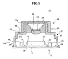
- FIG. 5 shows a semiconductor device (imaging apparatus) 10 manufactured by the manufacturing method according to the embodiment of the present invention.
- the description is given by taking the imaging apparatus 10 incorporating therein a semiconductor element (hereinafter referred to as "the optical sensor element 11") such as a CCD (charge coupled device) sensor or a CMOS sensor as a semiconductor device.
- the optical sensor element 11 such as a CCD (charge coupled device) sensor or a CMOS sensor
- the imaging apparatus 10 generally includes the optical sensor element 11, a substrate 12, and a holder 13, which serves as a sealing member.
- the optical sensor element 11 is, as mentioned above, a semiconductor element such as a CCD image sensor or a CMOS image sensor.
- the optical sensor element 11 is mounted on the substrate 12. More specifically, a control element 14 is mounted on the substrate 12, and the optical sensor element 11 is mounted on the control element 14.
- the control element 14 performs drive control of the optical sensor element 11.
- the optical sensor element 11 is connected to the control element 14 by means of wires 15.
- the control element 14 is electrically connected to the substrate 12 by means of wires 17.
- a passive element 16 such as a condenser is also mounted on the substrate 12.
- the holder 13 includes a lens holder 20, a housing 21, and a condenser lens 22, for example.
- the holder 13 is formed into a cylindrical shape and is provided with the condenser lens 22 therein.
- the condenser lens 22 serves to focus an image with respect to a photo-accepting surface of the optical sensor element 11 in a state where the holder 13 is mounted on the substrate 12.
- An aperture 23 for cutting unwanted light is provided on a top surface of the condenser lens 22.
- a cover glass 24 is provided at a top portion of the holder 13 that faces the condenser lens 22.
- the cover glass 24 is a cover for dust control and prevents dust from adhering to the condenser lens 22.
- the housing 21 includes a small diameter portion 21a and a large diameter portion 21b.
- a shoulder portion 21c is formed between the small diameter portion 21a and the large diameter portion 21b.
- a protruding screw portion is formed on the outer periphery of the small diameter portion 21a, and a receiving screw portion is formed on the inner periphery of the lens holder 20.
- the lens holder 20 is configured to be screwed to the small diameter portion 21a of the housing 21. In a state where the lens holder 20 is screwed to the housing 21, the lens holder 20 and the housing 21 form an airtight boundary.
- the bottom portion of the large diameter portion 21b is fixed to the substrate 12 by means of adhesive 28.
- an internal space 27 formed between the substrate 12 and the holder 13 is airtight. Accordingly, it is possible to prevent dust from adhering to the optical sensor element 11, which is located in the internal space 27.
- an air hole (opening) 25 is formed in the shoulder portion 21c, and the air hole 25 is closed with the adhesive 28.
- FIGS. 3A through 3C, 4A and 4B a description is given below of the manufacturing method of the imaging apparatus 10 having the above-mentioned structure. It should be noted that, in FIGS. 3A through 3C, 4A and 4B, only a part of the structure shown in FIG. 5 is illustrated so that the manufacturing method is easily understood.
- the optical sensor element 11 is mounted on the substrate 12.
- the passive element 16 is mounted, and bonding processes of the wires 15 and 17 are also performed.
- the adhesive 28 is deposited on the top surface of the substrate 12 at predetermined positions by using a dispenser 29.
- the positions at which the adhesive 29 is deposited are set so as to correspond to the shape of the bottom portion of the holder 13 (more specifically, the shape of the bottom portion of the large diameter portion 21b).
- a thermo-setting resin which provides a good bonding and achieves reliable bonding, is used as the adhesive 28.
- the bottom portion of the holder 13 is pressed against the substrate 12 at the positions where adhesive 28 is deposited.
- the holder 13 is temporarily fixed to the substrate 12.
- the substrate 12 on which the holder 13 is temporarily fixed is loaded in a curing apparatus and a curing process (heating process) is performed so as to cure the adhesive 28.
- the adhesive 28 is cured and the holder 13 is bonded to the substrate 12.
- the internal space 27 formed between the substrate 12 and the holder 13 is sealed with the optical sensor element 11 located therein.
- FIG. 4A shows the substrate 12 and the holder 13 during the curing process.
- the air inside the internal space 27 is heated and expanded.
- the air hole (opening) 25 is formed in the holder 13 in this embodiment.
- the internal space 25 communicates with the outside of the holder 13 via the air hole 25.
- the air in the internal space 27 formed between the substrate 12 and the holder 13 is heated and expanded, the air is discharged to the outside of the holder 13 via the air hole 25 (such air flows are indicated by arrows A in FIG. 4A). That is, the pressure in the internal space 27 becomes the same as the pressure outside the holder 13, and a pressure difference (air pressure difference) is not generated between the inside and outside of the holder 13 during the curing process. Accordingly, it is possible to prevent the bonding portion between the substrate 12 and the holder 13, more specifically, the portion bonded by means of the adhesive 28, from being damaged during the curing process.
- a process for closing the air hole 25 is subsequently performed.
- the process for closing the air hole 25 is performed after the temperatures of the substrate 12 and the holder 13 return to normal temperatures.
- the process for closing the air hole 25 is performed after such other heating processes are completed.
- the adhesive 28 is used in the process for closing the air hole 25.
- the adhesive 28 is an ultraviolet-curing type adhesive. By irradiating ultraviolet light to the air hole 25 after filling the air hole 25 with the adhesive 28 in a softened state, the adhesive 28 is cured in a short period of time.
- the ultraviolet-curing type adhesive 28 As in this embodiment, it is possible to cure the adhesive 28 in a short period of time by irradiation of ultraviolet light. It is conceivable that the pressure in the holder 13 (internal space 27) may vary since the temperature of the internal space 27 is increased by irradiation of ultraviolet light during the time period required for the adhesive 28 to be cured. However, since the air hole 25 is provided in this embodiment, the pressure in the holder 13 does not vary during the time period required for the adhesive 28 to be cured. Thus, it is possible to avoid faulty bonding.
- the adhesive 28 is not limited to the ultraviolet-curing type, and an instant adhesive that is cured in the air in a short period of time may be used instead.
- the internal space 27 is separated from the outside of the holder 13, and the optical sensor element 11 is located in the sealed internal space 27. Since the air hole 25 is closed after completion of the heating process performed in the manufacturing process of the imaging apparatus 10, a pressure difference between the inside and outside of the holder 13 is not generated after the internal space 27 having therein the optical sensor element 11 is sealed.
- the optical sensor element 11 (a CCD sensor or a CMOS sensor, for example) used in this embodiment is vulnerable to adhesion of dust. According to this embodiment, since it is possible to positively avoid entering of dust from the outside, it is possible to perform a good photoelectric conversion process by the optical sensor element 11 and improve reliability of the imaging apparatus 10.
- the air hole 25 is formed in the shoulder portion 21c of the holder 13 (housing 21). However, this is not a limitation of the position of the air hole 25.
- the air hole 25 may be formed in the large diameter portion 21b or the substrate 12.
- the air in the internal space 27 formed between the holder 13 and the substrate 12 communicates with the air outside the holder 13 (internal space 27).
- a pressure difference is not generated between the inside and outside the holder 13 (internal space 27). Accordingly, it is possible to prevent the bonding portion between the holder 13 and the substrate 12 from being damaged and maintain airtightness of the internal space 27. Thus, it is possible to improve reliability of the semiconductor device (imaging apparatus) 10.
Landscapes
- Engineering & Computer Science (AREA)
- Multimedia (AREA)
- Signal Processing (AREA)
- Solid State Image Pick-Up Elements (AREA)
- Encapsulation Of And Coatings For Semiconductor Or Solid State Devices (AREA)
- Light Receiving Elements (AREA)
- Transforming Light Signals Into Electric Signals (AREA)
- Studio Devices (AREA)
Abstract
Description
Claims (12)
- A manufacturing method of a semiconductor device in which method said semiconductor device is sealed by bonding a sealing member to a substrate mounting a semiconductor element thereon, said manufacturing method characterized by comprising the steps of:forming an opening in the sealing member; andclosing the opening after the sealing member having the opening formed therein is bonded to the substrate so as to seal the semiconductor device.
- The manufacturing method as claimed in claim 1, wherein the step of closing the opening is performed after heating processes of the semiconductor element, the substrate, and the sealing member end.
- The manufacturing method as claimed in claim 2, wherein the step of closing the opening is performed by using an adhesive.
- The manufacturing method as claimed in claim 3, wherein the semiconductor element is a photoelectric conversion element.
- The manufacturing method as claimed in claim 3, wherein the adhesive is an ultraviolet-curing type adhesive.
- The manufacturing method as claimed in claim 3, wherein the adhesive is an instant adhesive.
- The manufacturing method as claimed in claim 2, wherein the semiconductor element is a photoelectric conversion element
- The manufacturing method as claimed in claim 1, wherein the step of closing the opening is performed by using an adhesive.
- The manufacturing method as claimed in claim 8, wherein the semiconductor element is a photoelectric conversion element.
- The manufacturing method as claimed in claim 8, wherein the adhesive is an ultraviolet-curing type adhesive.
- The manufacturing method as claimed in claim 8, wherein the adhesive is an instant adhesive.
- The manufacturing method as claimed in claim 1, wherein the semiconductor element is a photoelectric conversion element.
Applications Claiming Priority (2)
| Application Number | Priority Date | Filing Date | Title |
|---|---|---|---|
| JP2003276961 | 2003-07-18 | ||
| JP2003276961A JP2005039152A (en) | 2003-07-18 | 2003-07-18 | Manufacturing method of semiconductor device |
Publications (2)
| Publication Number | Publication Date |
|---|---|
| EP1498959A2 true EP1498959A2 (en) | 2005-01-19 |
| EP1498959A3 EP1498959A3 (en) | 2007-06-20 |
Family
ID=33475586
Family Applications (1)
| Application Number | Title | Priority Date | Filing Date |
|---|---|---|---|
| EP04253509A Withdrawn EP1498959A3 (en) | 2003-07-18 | 2004-06-11 | Manufacturing method of a semiconductor device |
Country Status (6)
| Country | Link |
|---|---|
| US (1) | US6919218B2 (en) |
| EP (1) | EP1498959A3 (en) |
| JP (1) | JP2005039152A (en) |
| KR (1) | KR20050009666A (en) |
| CN (1) | CN100447967C (en) |
| TW (1) | TW200505232A (en) |
Cited By (2)
| Publication number | Priority date | Publication date | Assignee | Title |
|---|---|---|---|---|
| EP1796168A2 (en) | 2005-12-12 | 2007-06-13 | Robert Bosch Gmbh | Optical module and mounting method thereof |
| EP2750181A4 (en) * | 2011-08-22 | 2015-04-01 | Kyocera Corp | SEMICONDUCTOR OPTICAL DEVICE |
Families Citing this family (26)
| Publication number | Priority date | Publication date | Assignee | Title |
|---|---|---|---|---|
| JP4746358B2 (en) | 2005-06-09 | 2011-08-10 | 新光電気工業株式会社 | Semiconductor device and manufacturing method of semiconductor device |
| US20070145254A1 (en) * | 2005-12-28 | 2007-06-28 | Feng Chen | Packaging method for an assembly of image-sensing chip and circuit board |
| JP4852349B2 (en) * | 2006-06-13 | 2012-01-11 | 新光電気工業株式会社 | Semiconductor device and manufacturing method of semiconductor device |
| WO2008093463A1 (en) * | 2007-02-01 | 2008-08-07 | Konica Minolta Opto, Inc. | Imaging apparatus and portable terminal |
| CN101436603B (en) * | 2007-11-14 | 2010-11-10 | 鸿富锦精密工业(深圳)有限公司 | Imaging die set |
| CN101447474B (en) * | 2007-11-27 | 2011-03-30 | 鸿富锦精密工业(深圳)有限公司 | Image sensing wafer package structure and imaging module used by same |
| WO2009096460A1 (en) * | 2008-01-31 | 2009-08-06 | Konica Minolta Opto, Inc. | Imaging device, portable terminal, imaging device manufacturing method and portable terminal manufacturing method |
| US8538425B2 (en) * | 2008-07-01 | 2013-09-17 | Qualcomm Incorporated | Apparatus and method for improving mobile terminated cell setup performance during inter-frequency cell reselection |
| JP5376865B2 (en) * | 2008-08-19 | 2013-12-25 | キヤノン株式会社 | Solid-state imaging device and electronic imaging device |
| JP2010199302A (en) * | 2009-02-25 | 2010-09-09 | Sumitomo Electric Ind Ltd | Optical semiconductor device |
| WO2012008268A1 (en) * | 2010-07-14 | 2012-01-19 | コニカミノルタオプト株式会社 | Imaging device, and method for producing same |
| US8891007B2 (en) * | 2011-03-07 | 2014-11-18 | Digitaloptics Corporation | Camera module with protective air ventilation channel |
| CN102681299B (en) * | 2011-03-11 | 2016-07-06 | 鸿富锦精密工业(深圳)有限公司 | Camera module |
| KR20130087249A (en) * | 2012-01-27 | 2013-08-06 | 삼성전자주식회사 | Semiconductor apparatus and image sensor package using the same |
| JP5915265B2 (en) * | 2012-03-02 | 2016-05-11 | 日本電気株式会社 | Electronic component and method for manufacturing electronic component |
| CN104049311A (en) * | 2013-03-11 | 2014-09-17 | 鸿富锦精密工业(深圳)有限公司 | Optical-communication-module assembly device |
| KR102076339B1 (en) * | 2013-03-13 | 2020-02-11 | 삼성전자주식회사 | Semiconductor pakage and method of manufacturing the same |
| JP5700591B2 (en) * | 2013-07-31 | 2015-04-15 | 株式会社フジクラ | Dye-sensitized solar cell element |
| WO2016031332A1 (en) * | 2014-08-26 | 2016-03-03 | シャープ株式会社 | Camera module |
| US10009523B2 (en) * | 2015-05-11 | 2018-06-26 | Samsung Electro-Mechanics Co., Ltd. | Electronic module and method of manufacturing the same |
| JP6741933B2 (en) | 2015-10-02 | 2020-08-19 | ミツミ電機株式会社 | Optical scanning module, optical scanning control device |
| CN109994492A (en) * | 2017-12-29 | 2019-07-09 | 格科微电子(上海)有限公司 | CSP packaging method of image sensor |
| JP6738026B2 (en) * | 2018-08-23 | 2020-08-12 | ミツミ電機株式会社 | Optical scanning module and manufacturing method thereof |
| CN113784506B (en) * | 2020-06-10 | 2023-08-18 | 三赢科技(深圳)有限公司 | Lens module and electronic device |
| EP4357743B1 (en) | 2022-10-21 | 2025-06-25 | Aptiv Technologies AG | Method of monitoring reliability of system including electrical components |
| EP4357829A1 (en) * | 2022-10-21 | 2024-04-24 | Aptiv Technologies AG | Method for manufacturing an objective carrier assembly, objective carrier assembly for a camera, method for manufacturing a camera, and camera |
Family Cites Families (7)
| Publication number | Priority date | Publication date | Assignee | Title |
|---|---|---|---|---|
| US4897508A (en) * | 1988-02-10 | 1990-01-30 | Olin Corporation | Metal electronic package |
| US5059558A (en) * | 1988-06-22 | 1991-10-22 | North American Philips Corp., Signetics Division | Use of venting slots to improve hermetic seal for semiconductor dice housed in ceramic packages |
| US5081327A (en) * | 1990-03-28 | 1992-01-14 | Cabot Corporation | Sealing system for hermetic microchip packages |
| US5302778A (en) * | 1992-08-28 | 1994-04-12 | Eastman Kodak Company | Semiconductor insulation for optical devices |
| US5880403A (en) * | 1994-04-01 | 1999-03-09 | Space Electronics, Inc. | Radiation shielding of three dimensional multi-chip modules |
| JP2002185827A (en) | 2000-12-15 | 2002-06-28 | Matsushita Electric Ind Co Ltd | Board mounting camera |
| CN1445831A (en) * | 2002-03-18 | 2003-10-01 | 美新半导体(无锡)有限公司 | Cavity type packaging method for microelectronic circuits |
-
2003
- 2003-07-18 JP JP2003276961A patent/JP2005039152A/en active Pending
-
2004
- 2004-06-11 EP EP04253509A patent/EP1498959A3/en not_active Withdrawn
- 2004-06-14 TW TW093117051A patent/TW200505232A/en unknown
- 2004-06-15 US US10/868,513 patent/US6919218B2/en not_active Expired - Lifetime
- 2004-06-28 KR KR1020040048821A patent/KR20050009666A/en not_active Withdrawn
- 2004-06-30 CN CNB2004100617737A patent/CN100447967C/en not_active Expired - Fee Related
Cited By (3)
| Publication number | Priority date | Publication date | Assignee | Title |
|---|---|---|---|---|
| EP1796168A2 (en) | 2005-12-12 | 2007-06-13 | Robert Bosch Gmbh | Optical module and mounting method thereof |
| EP1796168A3 (en) * | 2005-12-12 | 2011-01-05 | Robert Bosch Gmbh | Optical module and mounting method thereof |
| EP2750181A4 (en) * | 2011-08-22 | 2015-04-01 | Kyocera Corp | SEMICONDUCTOR OPTICAL DEVICE |
Also Published As
| Publication number | Publication date |
|---|---|
| KR20050009666A (en) | 2005-01-25 |
| US20050014307A1 (en) | 2005-01-20 |
| TW200505232A (en) | 2005-02-01 |
| CN100447967C (en) | 2008-12-31 |
| US6919218B2 (en) | 2005-07-19 |
| CN1577776A (en) | 2005-02-09 |
| EP1498959A3 (en) | 2007-06-20 |
| JP2005039152A (en) | 2005-02-10 |
Similar Documents
| Publication | Publication Date | Title |
|---|---|---|
| US6919218B2 (en) | Manufacturing method for sealing a semiconductor device | |
| JP3646933B2 (en) | Solid-state imaging device and manufacturing method thereof | |
| KR100658150B1 (en) | Camera module and its manufacturing method | |
| JP2004007386A (en) | Image sensor module and method of manufacturing the same | |
| US10827606B2 (en) | Lens module having photosensitive chip embedded in through hole of circuit board and assembly method thereof | |
| CN1722456B (en) | Image sensor package and manufacturing method thereof | |
| US20080273111A1 (en) | Miniature camera module | |
| CN101494721B (en) | Image capturing module, method for manufacturing the image capturing module, and electronic information device | |
| WO2004107738A1 (en) | Imaging device and its manufacturing method | |
| US7442576B2 (en) | Placement of absorbing material in a semiconductor device | |
| CN108124082B (en) | Sinking type camera module, sinking type photosensitive assembly and manufacturing method thereof | |
| EP1708279A2 (en) | Optical device module, and method of fabricating the optical device module | |
| CN101518050A (en) | Solid-state image pickup device and method for manufacturing the same | |
| CN106998414B (en) | Image sensor module and camera module including the same | |
| KR100809682B1 (en) | Method for manufacturing optical device with transparent cover and method for manufacturing optical device module using same | |
| JP2001345391A (en) | Electronic component and method of manufacturing the same | |
| JP2003168793A (en) | Solid-state imaging device and method of manufacturing the same | |
| KR100818467B1 (en) | Camera module package | |
| KR101210159B1 (en) | Camera Module and Manufacturing Method thereof | |
| JP2002222935A (en) | Solid-state imaging device, manufacturing method thereof, and solid-state imaging system | |
| JP4578168B2 (en) | Method for manufacturing solid-state imaging device | |
| US20240387588A1 (en) | Image sensor packages and method thereof | |
| KR100840153B1 (en) | Camera module | |
| KR100584977B1 (en) | COB type image sensor module and manufacturing method thereof | |
| WO2007083564A1 (en) | Solid imaging device and manufacturing method thereof |
Legal Events
| Date | Code | Title | Description |
|---|---|---|---|
| PUAI | Public reference made under article 153(3) epc to a published international application that has entered the european phase |
Free format text: ORIGINAL CODE: 0009012 |
|
| AK | Designated contracting states |
Kind code of ref document: A2 Designated state(s): AT BE BG CH CY CZ DE DK EE ES FI FR GB GR HU IE IT LI LU MC NL PL PT RO SE SI SK TR |
|
| AX | Request for extension of the european patent |
Extension state: AL HR LT LV MK |
|
| RAP1 | Party data changed (applicant data changed or rights of an application transferred) |
Owner name: SHINKO ELECTRIC INDUSTRIES CO., LTD. |
|
| PUAL | Search report despatched |
Free format text: ORIGINAL CODE: 0009013 |
|
| AK | Designated contracting states |
Kind code of ref document: A3 Designated state(s): AT BE BG CH CY CZ DE DK EE ES FI FR GB GR HU IE IT LI LU MC NL PL PT RO SE SI SK TR |
|
| AX | Request for extension of the european patent |
Extension state: AL HR LT LV MK |
|
| 17P | Request for examination filed |
Effective date: 20070716 |
|
| 17Q | First examination report despatched |
Effective date: 20071221 |
|
| AKX | Designation fees paid |
Designated state(s): DE FI FR |
|
| STAA | Information on the status of an ep patent application or granted ep patent |
Free format text: STATUS: THE APPLICATION IS DEEMED TO BE WITHDRAWN |
|
| 18D | Application deemed to be withdrawn |
Effective date: 20100909 |