EP1494513A1 - Circuit board device for information apparatus, multilayered module board, and navigator - Google Patents
Circuit board device for information apparatus, multilayered module board, and navigator Download PDFInfo
- Publication number
- EP1494513A1 EP1494513A1 EP03745982A EP03745982A EP1494513A1 EP 1494513 A1 EP1494513 A1 EP 1494513A1 EP 03745982 A EP03745982 A EP 03745982A EP 03745982 A EP03745982 A EP 03745982A EP 1494513 A1 EP1494513 A1 EP 1494513A1
- Authority
- EP
- European Patent Office
- Prior art keywords
- board
- module board
- electronic components
- circuit board
- navigation system
- Prior art date
- Legal status (The legal status is an assumption and is not a legal conclusion. Google has not performed a legal analysis and makes no representation as to the accuracy of the status listed.)
- Withdrawn
Links
Images


Classifications
-
- H—ELECTRICITY
- H05—ELECTRIC TECHNIQUES NOT OTHERWISE PROVIDED FOR
- H05K—PRINTED CIRCUITS; CASINGS OR CONSTRUCTIONAL DETAILS OF ELECTRIC APPARATUS; MANUFACTURE OF ASSEMBLAGES OF ELECTRICAL COMPONENTS
- H05K1/00—Printed circuits
- H05K1/02—Details
- H05K1/14—Structural association of two or more printed circuits
- H05K1/141—One or more single auxiliary printed circuits mounted on a main printed circuit, e.g. modules, adapters
-
- H—ELECTRICITY
- H05—ELECTRIC TECHNIQUES NOT OTHERWISE PROVIDED FOR
- H05K—PRINTED CIRCUITS; CASINGS OR CONSTRUCTIONAL DETAILS OF ELECTRIC APPARATUS; MANUFACTURE OF ASSEMBLAGES OF ELECTRICAL COMPONENTS
- H05K3/00—Apparatus or processes for manufacturing printed circuits
- H05K3/46—Manufacturing multilayer circuits
-
- G—PHYSICS
- G01—MEASURING; TESTING
- G01C—MEASURING DISTANCES, LEVELS OR BEARINGS; SURVEYING; NAVIGATION; GYROSCOPIC INSTRUMENTS; PHOTOGRAMMETRY OR VIDEOGRAMMETRY
- G01C21/00—Navigation; Navigational instruments not provided for in groups G01C1/00 - G01C19/00
- G01C21/26—Navigation; Navigational instruments not provided for in groups G01C1/00 - G01C19/00 specially adapted for navigation in a road network
-
- H—ELECTRICITY
- H01—ELECTRIC ELEMENTS
- H01R—ELECTRICALLY-CONDUCTIVE CONNECTIONS; STRUCTURAL ASSOCIATIONS OF A PLURALITY OF MUTUALLY-INSULATED ELECTRICAL CONNECTING ELEMENTS; COUPLING DEVICES; CURRENT COLLECTORS
- H01R12/00—Structural associations of a plurality of mutually-insulated electrical connecting elements, specially adapted for printed circuits, e.g. printed circuit boards [PCB], flat or ribbon cables, or like generally planar structures, e.g. terminal strips, terminal blocks; Coupling devices specially adapted for printed circuits, flat or ribbon cables, or like generally planar structures; Terminals specially adapted for contact with, or insertion into, printed circuits, flat or ribbon cables, or like generally planar structures
- H01R12/50—Fixed connections
- H01R12/51—Fixed connections for rigid printed circuits or like structures
- H01R12/52—Fixed connections for rigid printed circuits or like structures connecting to other rigid printed circuits or like structures
-
- H—ELECTRICITY
- H05—ELECTRIC TECHNIQUES NOT OTHERWISE PROVIDED FOR
- H05K—PRINTED CIRCUITS; CASINGS OR CONSTRUCTIONAL DETAILS OF ELECTRIC APPARATUS; MANUFACTURE OF ASSEMBLAGES OF ELECTRICAL COMPONENTS
- H05K1/00—Printed circuits
- H05K1/02—Details
- H05K1/0213—Electrical arrangements not otherwise provided for
- H05K1/0237—High frequency adaptations
-
- H—ELECTRICITY
- H05—ELECTRIC TECHNIQUES NOT OTHERWISE PROVIDED FOR
- H05K—PRINTED CIRCUITS; CASINGS OR CONSTRUCTIONAL DETAILS OF ELECTRIC APPARATUS; MANUFACTURE OF ASSEMBLAGES OF ELECTRICAL COMPONENTS
- H05K1/00—Printed circuits
- H05K1/02—Details
- H05K1/0296—Conductive pattern lay-out details not covered by sub groups H05K1/02 - H05K1/0295
- H05K1/0298—Multilayer circuits
-
- H—ELECTRICITY
- H05—ELECTRIC TECHNIQUES NOT OTHERWISE PROVIDED FOR
- H05K—PRINTED CIRCUITS; CASINGS OR CONSTRUCTIONAL DETAILS OF ELECTRIC APPARATUS; MANUFACTURE OF ASSEMBLAGES OF ELECTRICAL COMPONENTS
- H05K2201/00—Indexing scheme relating to printed circuits covered by H05K1/00
- H05K2201/10—Details of components or other objects attached to or integrated in a printed circuit board
- H05K2201/10007—Types of components
- H05K2201/10159—Memory
-
- H—ELECTRICITY
- H05—ELECTRIC TECHNIQUES NOT OTHERWISE PROVIDED FOR
- H05K—PRINTED CIRCUITS; CASINGS OR CONSTRUCTIONAL DETAILS OF ELECTRIC APPARATUS; MANUFACTURE OF ASSEMBLAGES OF ELECTRICAL COMPONENTS
- H05K2201/00—Indexing scheme relating to printed circuits covered by H05K1/00
- H05K2201/10—Details of components or other objects attached to or integrated in a printed circuit board
- H05K2201/10007—Types of components
- H05K2201/10189—Non-printed connector
-
- H—ELECTRICITY
- H05—ELECTRIC TECHNIQUES NOT OTHERWISE PROVIDED FOR
- H05K—PRINTED CIRCUITS; CASINGS OR CONSTRUCTIONAL DETAILS OF ELECTRIC APPARATUS; MANUFACTURE OF ASSEMBLAGES OF ELECTRICAL COMPONENTS
- H05K2201/00—Indexing scheme relating to printed circuits covered by H05K1/00
- H05K2201/10—Details of components or other objects attached to or integrated in a printed circuit board
- H05K2201/10227—Other objects, e.g. metallic pieces
- H05K2201/10424—Frame holders
-
- H—ELECTRICITY
- H05—ELECTRIC TECHNIQUES NOT OTHERWISE PROVIDED FOR
- H05K—PRINTED CIRCUITS; CASINGS OR CONSTRUCTIONAL DETAILS OF ELECTRIC APPARATUS; MANUFACTURE OF ASSEMBLAGES OF ELECTRICAL COMPONENTS
- H05K2201/00—Indexing scheme relating to printed circuits covered by H05K1/00
- H05K2201/10—Details of components or other objects attached to or integrated in a printed circuit board
- H05K2201/10613—Details of electrical connections of non-printed components, e.g. special leads
- H05K2201/10621—Components characterised by their electrical contacts
- H05K2201/10689—Leaded Integrated Circuit [IC] package, e.g. dual-in-line [DIL]
-
- H—ELECTRICITY
- H05—ELECTRIC TECHNIQUES NOT OTHERWISE PROVIDED FOR
- H05K—PRINTED CIRCUITS; CASINGS OR CONSTRUCTIONAL DETAILS OF ELECTRIC APPARATUS; MANUFACTURE OF ASSEMBLAGES OF ELECTRICAL COMPONENTS
- H05K2203/00—Indexing scheme relating to apparatus or processes for manufacturing printed circuits covered by H05K3/00
- H05K2203/15—Position of the PCB during processing
- H05K2203/1572—Processing both sides of a PCB by the same process; Providing a similar arrangement of components on both sides; Making interlayer connections from two sides
-
- H—ELECTRICITY
- H05—ELECTRIC TECHNIQUES NOT OTHERWISE PROVIDED FOR
- H05K—PRINTED CIRCUITS; CASINGS OR CONSTRUCTIONAL DETAILS OF ELECTRIC APPARATUS; MANUFACTURE OF ASSEMBLAGES OF ELECTRICAL COMPONENTS
- H05K3/00—Apparatus or processes for manufacturing printed circuits
- H05K3/30—Assembling printed circuits with electric components, e.g. with resistors
- H05K3/32—Assembling printed circuits with electric components, e.g. with resistors electrically connecting electric components or wires to printed circuits
- H05K3/34—Assembling printed circuits with electric components, e.g. with resistors electrically connecting electric components or wires to printed circuits by soldering
- H05K3/341—Surface mounted components
- H05K3/3421—Leaded components
-
- H—ELECTRICITY
- H05—ELECTRIC TECHNIQUES NOT OTHERWISE PROVIDED FOR
- H05K—PRINTED CIRCUITS; CASINGS OR CONSTRUCTIONAL DETAILS OF ELECTRIC APPARATUS; MANUFACTURE OF ASSEMBLAGES OF ELECTRICAL COMPONENTS
- H05K3/00—Apparatus or processes for manufacturing printed circuits
- H05K3/36—Assembling printed circuits with other printed circuits
- H05K3/368—Assembling printed circuits with other printed circuits parallel to each other
Definitions
- the present invention relates to a circuit board structure in an information apparatus ideal in applications such as an on-vehicle information terminal having a navigation function.
- On-vehicle information terminals in the known art that have navigation functions including a function for displaying a road map of an area around the current vehicle position, a function for determining a recommended route from a start point to a destination through arithmetic operation and a function for providing route guidance based upon the recommended route determined through the arithmetic operation.
- Such an on-vehicle information terminal includes a navigation circuit board.
- the navigation circuit board is achieved by mounting on a single multilayer printed board a plurality of low-frequency electronic components such as a power circuit, a gyro, a GPS circuit and a plurality of high-frequency electronic components such as a CPU chip, a memory chip and a graphics chip.
- the navigation circuit board Since the navigation specifications vary among different vehicle models, the navigation circuit board is designed and manufactured in conformance to each set of specifications in the related art. This means a great length of time must be spent in the design stage to result in high production costs, and it is naturally more desirable to use fewer types of more versatile navigation circuit boards. Such a need is not unique to navigation circuit boards, but it is a common concern pertaining to all types of information terminals including on-vehicle information terminals, in which a given function needs to be altered for different models.
- the present invention provides a circuit board structure to be adopted in an information apparatus that eliminates the need to design and manufacture the circuit board from scratch for each set of specifications.
- the circuit board device for an information apparatus comprises a base board having a plurality of electronic components mounted thereupon and a multilayer module board mounted at one surface of the base board and having mounted thereupon a plurality of electronic components including at least a CPU and a memory.
- the multilayer module board is a multilayered board smaller in size than the base board, and the plurality of electronic components are wired through a wiring pattern at an inner layer of the multilayer board.
- the multilayer module board may be connected to the base board by soldering a connector terminal provided at a peripheral edge thereof onto a junction portion formed on the base board.
- the high-frequency electronic circuits include at least a graphics circuit as well as the CPU and the memory.
- the low-frequency electronic circuits include at least a power circuit, a gyro and a GPS circuit.
- the circuit board device described above may be adopted in a navigation system.
- a plurality of high-frequency electronic components including the CPU and the memory are mounted at, at least, a surface thereof on one side, and the plurality of high-frequency electronic components are connected with one another through a wiring pattern formed at an inner layer.
- the overall shape of this module board may be rectangular.
- Connector terminals provided as separate members may each be connected through soldering onto one of the four peripheral edges of the board.
- the four connector terminals at such a multilayer module board each include a narrow elongated base portion constituted of resin and a plurality of pins fixed to the base portion and the four connector terminals are carried with the base portions mounted at a transfer adapter and are connected through soldering onto the rear surface of the board while attached to the transfer adapter.
- the multilayer module board may adopt the structure described below.
- the four connector terminals may each include a narrow, elongated base portion constituted of resin, a plurality of pins fixed to the base portion, aligning pins projecting at both ends of the base portion to be used when soldering the connector terminal onto the rear surface of the board, and inclined surfaces for position control formed at both ends of the base portion to be used when soldering the connector terminal.
- a pair of positioning holes at which the aligning pins can be loosely fitted may be formed.
- This structure allows the position control inclined surfaces of adjacent connector terminals to come into contact with each other in a state in which the aligning pins are loosely fitted at the positioning holes, and thus, it becomes possible to control the positions of the connector terminals when connecting them to the board through soldering.
- Module boards include, at least, a high-speed module board, an advanced function module board, a low-end module board and a multimedia module board having a non-navigation function that allows various types of data such as music and images to be reproduced as well as a navigation function.
- a single common base board can be used in conjunction with a plurality of module boards and the circuit board is manufactured by mounting one module board selected from the plurality of module boards at the base board.
- the high-speed module board is a circuit board for a high-grade navigation system that operates at higher speed rather than a navigation system conforming to low-end specifications.
- the advanced function module board is a circuit board for a high-grade navigation system having more functions than a navigation system conforming to low-end specifications.
- the low-end module board is a circuit board for a less expensive navigation system conforming to lower end specifications rather than the high-grade navigation system.
- the need to design and manufacture a circuit board for each set of specifications from scratch is eliminated and thus, the length of time to be spent in the development stage is reduced to achieve a cost reduction.
- FIG. 1 is a system block diagram of a navigation system 10 achieved in an embodiment of the present invention.
- the navigation system 10 has functions for providing information related to vehicle travel. More specifically, it has a function for displaying a road map of an area around the current vehicle position, a function for calculating a recommended route from the start point (the current position) to a destination (an end point) through arithmetic operation, a function for providing route guidance based upon the calculated recommended route and the like. In short, it is an apparatus that provides so-called navigation or route guidance.
- Reference numeral 11 in FIG. 1 indicates a current position detection device that detects the current position of the vehicle, which may include, for instance, a gyro 11a that detects the advancing direction of the vehicle, a vehicle speed sensor 11b that detects the vehicle speed and a GPS circuit 11c that detects a GPS signal provided from a GPS satellite.
- Reference numeral 12 indicates a map storage memory in which road map data, address data and the like readout by a read device from a recording medium such as a CD-ROM 13 or a DVD are stored as needed.
- Reference numeral 14 indicates a control circuit that controls the overall system and comprises a microprocessor and its peripheral circuits.
- the control circuit 14 uses a RAM 15 as a work area where it implements various types of control to be detailed later by executing a control program stored in a ROM 16.
- Reference numeral 17 indicates a graphics circuit that executes, for instance, drawing processing when displaying a planimetric map, a stereoscopic map (a birds-eye-view map) or the like at a monitor 19.
- Reference numeral 18 indicates an image memory in which image data to be displayed at the display monitor 19 are stored.
- the image data which include road map drawing data and various types of graphics data, are prepared at the graphics circuit 17.
- the image data stored in the image memory 18 are read out as needed and are displayed at the display monitor 19.
- Reference numeral 20 indicates an ASIC that executes processing such as a route search calculation.
- the navigation system 10 adopting the structure described above executes a route search by designating the subject vehicle position detected by the current position detection device 11 as the start point and designating the destination set by the operator as the end point.
- the route search is executed by adopting a method of the known art based upon the road map data stored in the CD-ROM 13 or the map storage memory 12.
- the route resulting from the search is displayed with a bold line on the display monitor 19 and the vehicle is guided to the destination by providing audio guidance whenever the vehicle approaches a right or left turn point.
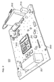
- FIG. 2 is a perspective of a circuit board device 100 of the navigation system 10
- FIG. 3 shows the circuit board device 100 viewed from the front
- FIG. 4 shows the circuit board device 100 viewed from the rear.
- the circuit board device 100 includes a multilayer base board 200 having a plurality of electronic components mounted thereupon and a multilayer module board 300 mounted at the base board 200 and having mounted thereupon a plurality of electronic components including at least a CPU and a memory.
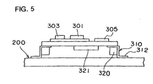
- the multilayer module board 300 is connected to the base board 200 by soldering connector terminals 310 disposed at peripheral edges thereof to junction portions formed at the base board 200.
- a plurality of wiring pattern layers are formed in the base board 200, and a power device 201, a GPS circuit 202, a gyro 203 and other electronic components are mounted at the top layer (the front surface) of the base board 200. At the bottom layer (the rear surface) of the base board 200, connector devices 204 and other electronic components are mounted.
- the electronic components mounted at the base board 200 are all low-frequency components connected with one another through the wiring patterns formed at inner wiring pattern layers. It is to be noted that while electronic components having operating frequencies equal to or lower than 40MHz are defined as the low-frequency electronic components in the explanation of the embodiment, low-frequency electronic components may operate at other operating frequencies.
- the multilayer module board 300 assuming a square shape includes a plurality of wiring pattern layers.
- a plurality of high-frequency electronic components such as a CPU 301, an ASIC 302, a memory 303, a graphics circuit 304 and a flash memory 305 are mounted at the top layer (the front surface) of the multilayer module board 300.
- the CPU 301, the ASIC 302, the memory 303, the graphics circuit 304 and like with operating frequencies equal to or higher than 200MHz are provided in a so-called multi-chip module.
- These high-speed elements are connected with one another through a wiring pattern formed at an inner layer of the multi-chip module.
- the operating frequencies of elements that are not part of the multi-chip module, such as the flash memory 305, are equal to or higher than 100MHz and equal to or lower than 200MHz, and these elements are connected with one another at an inner pattern layer in the multilayer module 300. It is to be noted that the high-frequency electronic components may operate at operating frequencies other than those mentioned above.
- the length of the wiring required to connect the high-frequency electronic components can be reduced compared to the length of wiring that would be required to connect them all at the front surface of the multilayer module board 300, which will approve effective when adopted in conjunction with EMI. It is to be noted that while electronic components that operate at operating frequencies equal to or higher than 100MHz are defined as high-frequency electronic components in the explanation of the embodiment, the high-frequency electronic components may operate at other frequencies.
- a specific clearance is formed by the connector terminals 310 between the rear surface of the multilayer module board 300 and the base board 200.
- a plurality of electronic components 320, 321,... can be mounted at the bottom layer (rear surface) of the multilayer module board 300.
- FIG. 6 is a bottom view of the multilayer module board 300.
- connector terminals 310a to 310d they may be collectively referred to by using reference numeral 310) are each connected through soldering to one of the four sides at the rear surface of the multilayer module board 300.
- the connector terminals 310a to 310d are attached to a transfer adapter 400, as shown in FIG. 7, the multilayer module board 300 is handled by vacuum holding the transfer adapter 400 with a handling device, and the multilayer module board 300 is then soldered onto the base board 200.
- the transfer adapter 400 is also used when connecting through soldering the connector terminals 310a to 310d to the multilayer module board 300 to improve the ease of the soldering operation.
- the transfer adapter 400 is to be detailed later.
- the four connector terminals 310 each include a narrow, elongated base portion 311 constituted of resin, a plurality of pins 312 fixed onto the base portion 311, aligning pins 313 (see FIG. 11) each projecting at the front surface of the base portion 311 at one of the two ends thereof, i.e., on the reverse side of the view shown in FIG.
- inclined surfaces 314 for position control each formed at one of the two ends of the base portion 311 to be used when connecting the connector terminal through soldering
- fitting connection portions 315 and 316 each located at one of the two ends of the base portion 311 to connect with the transfer adapter 400 and connecting grooves 317 at which positioning projections 411 (see FIG. 9) of the transfer adapter 400 are inserted.
- the transfer adapter 400 includes an outer perimeter portion 410 substantially assuming the shape of a closed rectangle and a cross portion assuming a cross shape that connects the sides of the outer perimeter portion 410 to one another.
- FIG. 9 is a perspective of a corner area of the transfer adapter 400. As shown in FIG. 9, at a corner of the outer perimeter portion 410, a projection 411 that is inserted in connecting grooves 317 of connector terminals 310, outer connection claws 412 which connect with the fitting connection portion 315 of a connector terminal 310 and inner connection claws 413 which connect with the fitting connection portion 316 of a connector terminal 310 are provided.
- a pair of positioning holes 306 at which the aligning pins 313 of the multilayer module board 300 are loosely fitted are formed.
- the four connector terminals 310 each become snapped onto the transfer adapter 400. While the widthwise movement of the connector terminals 310 having become snapped onto the transfer adapter 400 is restricted inside the transfer adapter 400, they are held with a degree of freedom of movement along other directions.
- the transfer adapter 400 is handled with a transfer device, the transfer adapter 400 is positioned in this state onto the rear surface of the multilayer module board 300 and the connector terminals 310 are then soldered onto the multilayer module board 300.
- the aligning pins 313 in the connector terminals 310 are designed so as to have a predetermined degree of play relative to the positioning holes 306 at the multilayer module board 300.
- the aligning pins 313 of the connector terminals 310 are fitted into the positioning holes 306 at the multilayer module board 300, as shown in FIG. 11.
- the connector terminals 310 are soldered onto the multilayer module board 300 in this state. Since the pins 313 are fitted in the holes 306 with play, the connector terminals 310 attached to the transfer adapter 400 may still move inside the transfer adapter 400.
- the positions of the connector terminals 310 are controlled in the embodiment as the position control inclined surfaces 314 of, for instance, the adjacent connector terminals 310b and 310c come into contact with each other, as shown in FIG. 8.
- the connector terminals 310 are positioned at the individual sides of the module board 300 within an allowable range and the connector terminals 310 are connected through soldering onto the multilayer module board 300 via the pins 312 in this state.
- such a module board 300 is connected through soldering onto the base board 200 together with other electronic components by vacuum holding the transfer adapter 400 attached to the connector terminals 310a to 310d with the handling device.
- the circuit board device according to the present invention may be adopted in conjunction with a portable navigation system or any other type of information apparatus.
- the embodiment explained above simply represents an example and the present invention may be adopted in a circuit board device achieved in any of various modes without being subject to any restrictions set forth in the embodiment.
- the use of a transfer adapter, connector terminals or a multi-chip module is not essential to the implementation of the invention.
- the types of low-frequency electronic components and high-frequency electronic components, too, are not limited to those used in the embodiment.
Landscapes
- Engineering & Computer Science (AREA)
- Radar, Positioning & Navigation (AREA)
- Remote Sensing (AREA)
- Microelectronics & Electronic Packaging (AREA)
- Automation & Control Theory (AREA)
- Physics & Mathematics (AREA)
- General Physics & Mathematics (AREA)
- Manufacturing & Machinery (AREA)
- Combinations Of Printed Boards (AREA)
- Structures For Mounting Electric Components On Printed Circuit Boards (AREA)
Abstract
Description
Japanese Patent Application No. 2002-106513
Claims (13)
- A circuit board device for an information apparatus comprising:a base board having mounted thereupon a plurality of electronic components; anda multilayer module board mounted at one surface of the base board and having mounted thereupon a plurality of electronic components including at least a CPU and a memory, wherein:the multilayer module board is a multilayered board smaller in size than the base board, and the plurality of electronic components are wired to one another through a wiring pattern at an inner layer of the multilayer board.
- A circuit board device for an information apparatus according to claim 1, wherein:the multilayer module board is connected to the base board by soldering a connector terminal disposed at a peripheral edge thereof to a junction portion formed on the base board.
- A circuit board device for an information apparatus according to claim 2, wherein:an electronic component is mounted at another surface of the multilayer module board, separated from the electronic components mounted at one surface of the multilayer module board, by utilizing a space formed by the connector terminal between the multilayer module board and the base board.
- A circuit board device for an information apparatus according to any of claims 1 through 3, wherein:the electronic components mounted at the base board are low-frequency electronic components and the electronic components mounted at the multilayer module board are high-frequency electronic components.
- A circuit board device for an information apparatus according to any of claims 1 through 4, wherein:the high-frequency electronic circuits include at least a graphics circuit, in addition to the CPU and the memory.
- A circuit board device for an information apparatus according to claim 4, wherein:the low-frequency electronic circuits include at least a power circuit, a gyro and a GPS circuit.
- A navigation system comprising a circuit board device according to any of claims 1 through 6.
- A multilayer module board, comprising:a plurality of high-frequency electronic components including a CPU and a memory mounted at, at least, one surface thereof, wherein:the plurality of high-frequency electronic components are connected with one another through a wiring pattern formed at an inner layer.
- A multilayer module board according to claim 8, assuming an overall shape of a rectangle and having connector terminals provided as separate members each soldered onto one of four peripheral edges thereof.
- A multilayer module board according to claim 9, wherein:the four connector terminals each include a narrow, elongated base portion constituted of resin and a plurality of pins fixed to the base portion; andafter the four connector terminals are each carried with the base portion attached to a transfer adapter, the four connector terminals are connected through soldering onto a rear surface of the board while attached to the transfer adapter.
- A multilayer module board according to claim 9, wherein:the four connector terminals each include;a narrow, elongated base portion constituted of resin;a plurality of pins fixed to the base portion;aligning pins projecting at both ends of the base portion to be used when soldering the connector terminal onto a rear surface of the board; andinclined surfaces for position control formed at both ends of the base portion to be used when soldering the connector terminal;a pair of positioning holes at which the aligning pins are loosely fitted are formed at each of four corners of the board; andpositions of the connector terminals are controlled when soldering the connector terminals as the inclined surfaces for position control at adjacent connector terminals come into contact with each other while the positioning pins are loosely fitted at the positioning holes.
- A circuit board for a navigation system achieved by mounting a module board according to any of claims 1 through 11 at a base board according to any of claims 1 through 11, wherein:the module board is one of at least a high-speed module board, an advanced function module board, a low-end module board and a multimedia module board having a function for reproducing various types of data such as music and images as well as a navigation function; andthe base board is used commonly in conjunction with the plurality of module boards.
- A circuit board for a navigation system according to claim 12, wherein:the high-speed module board is a circuit board for a high-grade navigation system that operates at higher speed than a navigation system conforming to low-end specifications;the advanced function module board is a circuit board for a high-grade navigation system having more functions than a navigation system conforming to low-end specifications; andthe low-end module board is a circuit board for a less expensive navigation system conforming to lower-end specifications rather than the high-grade navigation system.
Applications Claiming Priority (3)
| Application Number | Priority Date | Filing Date | Title |
|---|---|---|---|
| JP2002106513 | 2002-04-09 | ||
| JP2002106513A JP4209130B2 (en) | 2002-04-09 | 2002-04-09 | Multilayer module board |
| PCT/JP2003/004489 WO2003086035A1 (en) | 2002-04-09 | 2003-04-09 | Circuit board device for information apparatus, multilayered module board, and navigator |
Publications (2)
| Publication Number | Publication Date |
|---|---|
| EP1494513A1 true EP1494513A1 (en) | 2005-01-05 |
| EP1494513A4 EP1494513A4 (en) | 2010-04-07 |
Family
ID=28786429
Family Applications (1)
| Application Number | Title | Priority Date | Filing Date |
|---|---|---|---|
| EP03745982A Withdrawn EP1494513A4 (en) | 2002-04-09 | 2003-04-09 | Circuit board device for information apparatus, multilayered module board, and navigator |
Country Status (6)
| Country | Link |
|---|---|
| US (1) | US7869223B2 (en) |
| EP (1) | EP1494513A4 (en) |
| JP (1) | JP4209130B2 (en) |
| KR (1) | KR100744898B1 (en) |
| CN (1) | CN100370225C (en) |
| WO (1) | WO2003086035A1 (en) |
Families Citing this family (7)
| Publication number | Priority date | Publication date | Assignee | Title |
|---|---|---|---|---|
| JP4930070B2 (en) * | 2007-01-23 | 2012-05-09 | 横河電機株式会社 | Printed wiring board |
| JP2010282702A (en) * | 2009-06-05 | 2010-12-16 | Elpida Memory Inc | Memory module |
| DE102013001006B4 (en) * | 2013-01-22 | 2015-01-22 | Baumüller Nürnberg GmbH | Printed circuit board assembly |
| JP6331266B2 (en) * | 2013-05-24 | 2018-05-30 | セイコーエプソン株式会社 | Sensor unit, electronic device and moving body |
| JP6221597B2 (en) * | 2013-10-04 | 2017-11-01 | セイコーエプソン株式会社 | Sensor unit, electronic device and moving body |
| CN110446340A (en) * | 2018-05-06 | 2019-11-12 | 马春辉 | Modular combination circuit board and its method for manufacturing |
| KR101927950B1 (en) * | 2018-07-09 | 2018-12-12 | 김만영 | Printed circuit board based on processor module |
Family Cites Families (31)
| Publication number | Priority date | Publication date | Assignee | Title |
|---|---|---|---|---|
| JPS6294670A (en) * | 1985-10-18 | 1987-05-01 | 白木金属工業株式会社 | Electronic key apparatus |
| JPS6294670U (en) * | 1985-12-04 | 1987-06-17 | ||
| JPH07107956B2 (en) * | 1988-02-29 | 1995-11-15 | 沖電気工業株式会社 | Processor built-in circuit |
| US5025306A (en) * | 1988-08-09 | 1991-06-18 | Texas Instruments Incorporated | Assembly of semiconductor chips |
| US5191404A (en) * | 1989-12-20 | 1993-03-02 | Digital Equipment Corporation | High density memory array packaging |
| JPH0486979A (en) | 1990-07-31 | 1992-03-19 | Toshiba Corp | Automatic ticket examining system |
| JPH0496979U (en) * | 1991-02-01 | 1992-08-21 | ||
| DE4108154A1 (en) * | 1991-03-14 | 1992-09-17 | Telefunken Electronic Gmbh | ELECTRONIC ASSEMBLY AND METHOD FOR PRODUCING ELECTRONIC ASSEMBLIES |
| TW212261B (en) * | 1992-03-09 | 1993-09-01 | Matsushita Electric Industrial Co Ltd | Electronic circuit device and manufacturing method |
| JPH066027A (en) * | 1992-06-22 | 1994-01-14 | Matsushita Electric Ind Co Ltd | Manufacturing method of circuit module |
| JPH06204642A (en) | 1992-12-28 | 1994-07-22 | Matsushita Electric Ind Co Ltd | Electronic circuit device |
| JP2692522B2 (en) * | 1993-02-16 | 1997-12-17 | 日立電線株式会社 | Package module board |
| JP2750998B2 (en) | 1993-12-29 | 1998-05-18 | 日本航空電子工業株式会社 | Mounting connector |
| TW256013B (en) * | 1994-03-18 | 1995-09-01 | Hitachi Seisakusyo Kk | Installation board |
| EP0717443B1 (en) * | 1994-07-04 | 1999-03-03 | Matsushita Electric Industrial Co., Ltd. | Integrated circuit device |
| JP2692619B2 (en) * | 1994-11-24 | 1997-12-17 | 日本電気株式会社 | Wireless transceiver |
| US5761051A (en) | 1994-12-29 | 1998-06-02 | Compaq Computer Corporation | Multi-layer circuit board having a supply bus and discrete voltage supply planes |
| US5610801A (en) * | 1995-03-20 | 1997-03-11 | Intel Corporation | Motherboard assembly which has a single socket that can accept a single integrated circuit package or multiple integrated circuit packages |
| US5657208A (en) * | 1995-07-28 | 1997-08-12 | Hewlett-Packard Company | Surface mount attachments of daughterboards to motherboards |
| JP3493254B2 (en) * | 1995-09-20 | 2004-02-03 | 株式会社日立製作所 | Portable wireless terminal |
| KR100355263B1 (en) * | 1995-09-05 | 2002-12-31 | 가부시끼가이샤 히다치 세이사꾸쇼 | Coaxial Resonant Slot Antenna, Manufacturing Method and Portable Wireless Terminal |
| EP1426910A3 (en) * | 1996-04-16 | 2006-11-02 | Xanavi Informatics Corporation | Map display device, navigation device and map display method |
| JPH10141496A (en) * | 1996-10-25 | 1998-05-29 | Aqueous Res:Kk | Vehicle control device |
| US5825630A (en) * | 1996-11-07 | 1998-10-20 | Ncr Corporation | Electronic circuit board including a second circuit board attached there to to provide an area of increased circuit density |
| JPH11119862A (en) | 1997-10-09 | 1999-04-30 | Canon Inc | Printed wiring board unit and electronic equipment |
| US6477593B1 (en) * | 1998-06-11 | 2002-11-05 | Adaptec, Inc. | Stacked I/O bridge circuit assemblies having flexibly configurable connections |
| DE19852659B4 (en) | 1998-11-16 | 2009-12-24 | Robert Bosch Gmbh | Navigation with multimedia |
| JP2001135904A (en) | 1999-11-04 | 2001-05-18 | Ricoh Co Ltd | Module board mounting structure and module board |
| JP2001196792A (en) * | 2000-01-13 | 2001-07-19 | Denso Corp | How to mount electronic components on flexible substrates |
| JP3900778B2 (en) | 2000-02-22 | 2007-04-04 | アイシン・エィ・ダブリュ株式会社 | Navigation device |
| JP2001251060A (en) | 2000-03-02 | 2001-09-14 | Sony Corp | Multilayer type printed wiring board |
-
2002
- 2002-04-09 JP JP2002106513A patent/JP4209130B2/en not_active Expired - Fee Related
-
2003
- 2003-04-09 WO PCT/JP2003/004489 patent/WO2003086035A1/en not_active Ceased
- 2003-04-09 KR KR1020047016078A patent/KR100744898B1/en not_active Expired - Fee Related
- 2003-04-09 CN CNB038077760A patent/CN100370225C/en not_active Expired - Fee Related
- 2003-04-09 EP EP03745982A patent/EP1494513A4/en not_active Withdrawn
- 2003-04-09 US US10/510,567 patent/US7869223B2/en not_active Expired - Fee Related
Also Published As
| Publication number | Publication date |
|---|---|
| KR20040097327A (en) | 2004-11-17 |
| US20050156306A1 (en) | 2005-07-21 |
| US7869223B2 (en) | 2011-01-11 |
| KR100744898B1 (en) | 2007-08-01 |
| EP1494513A4 (en) | 2010-04-07 |
| CN1669370A (en) | 2005-09-14 |
| WO2003086035A1 (en) | 2003-10-16 |
| JP2003304046A (en) | 2003-10-24 |
| CN100370225C (en) | 2008-02-20 |
| JP4209130B2 (en) | 2009-01-14 |
Similar Documents
| Publication | Publication Date | Title |
|---|---|---|
| US11709079B2 (en) | Sensor device and electronic apparatus | |
| US7339646B2 (en) | Connection structures of wiring board and connection structure of liquid crystal display panel | |
| US20050038597A1 (en) | Sensing apparatus for a navigation system | |
| US7869223B2 (en) | Circuit board device for information apparatus, multilayered module board and navigation system | |
| JP2006308498A (en) | Angular velocity sensor | |
| CA2954343C (en) | Display unit for vehicle and display control unit | |
| JP3900778B2 (en) | Navigation device | |
| US11013106B1 (en) | Electronic control unit | |
| US20050097583A1 (en) | Complex electronic device having circuit board for operation button control and device units connected by bent or folded flexible flat cables | |
| JP7635084B2 (en) | Imaging device | |
| WO2021157629A1 (en) | Electronic device | |
| EP1703780B1 (en) | Printed wiring board with an FPC connector | |
| JP2004170380A (en) | Orthogonal triaxial acceleration measuring instrument | |
| JP7095850B2 (en) | Cable routing structure and cable routing method | |
| JP4511333B2 (en) | Sensor-equipped modules and electronic components | |
| EP0893208A2 (en) | An orthogonal type three-axis robot and a control method thereof | |
| JP2001183162A (en) | Attitude angle detector | |
| JP2606174B2 (en) | Mounting method of two-story electronic circuit package | |
| JPH03152984A (en) | flexible circuit board | |
| JPH069314Y2 (en) | Panel mount type controller | |
| JP2012033789A (en) | Electronic apparatus | |
| JPH09223900A (en) | Parts mounting machine | |
| JP2003218477A (en) | Circuit board | |
| JPH1011917A (en) | Head unit for optical deck and assembly method | |
| JPH0582070U (en) | Printed circuit board |
Legal Events
| Date | Code | Title | Description |
|---|---|---|---|
| PUAI | Public reference made under article 153(3) epc to a published international application that has entered the european phase |
Free format text: ORIGINAL CODE: 0009012 |
|
| 17P | Request for examination filed |
Effective date: 20041101 |
|
| AK | Designated contracting states |
Kind code of ref document: A1 Designated state(s): AT BE BG CH CY CZ DE DK EE ES FI FR GB GR HU IE IT LI LU MC NL PT RO SE SI SK TR |
|
| A4 | Supplementary search report drawn up and despatched |
Effective date: 20100310 |
|
| 17Q | First examination report despatched |
Effective date: 20101020 |
|
| STAA | Information on the status of an ep patent application or granted ep patent |
Free format text: STATUS: EXAMINATION IS IN PROGRESS |
|
| STAA | Information on the status of an ep patent application or granted ep patent |
Free format text: STATUS: THE APPLICATION IS DEEMED TO BE WITHDRAWN |
|
| 18D | Application deemed to be withdrawn |
Effective date: 20181101 |