JP2010282702A - Memory module - Google Patents
Memory module Download PDFInfo
- Publication number
- JP2010282702A JP2010282702A JP2009136647A JP2009136647A JP2010282702A JP 2010282702 A JP2010282702 A JP 2010282702A JP 2009136647 A JP2009136647 A JP 2009136647A JP 2009136647 A JP2009136647 A JP 2009136647A JP 2010282702 A JP2010282702 A JP 2010282702A
- Authority
- JP
- Japan
- Prior art keywords
- data
- memory
- command
- address
- register buffer
- Prior art date
- Legal status (The legal status is an assumption and is not a legal conclusion. Google has not performed a legal analysis and makes no representation as to the accuracy of the status listed.)
- Withdrawn
Links
Images


Classifications
-
- G—PHYSICS
- G11—INFORMATION STORAGE
- G11C—STATIC STORES
- G11C5/00—Details of stores covered by group G11C11/00
- G11C5/02—Disposition of storage elements, e.g. in the form of a matrix array
- G11C5/04—Supports for storage elements, e.g. memory modules; Mounting or fixing of storage elements on such supports
-
- G—PHYSICS
- G11—INFORMATION STORAGE
- G11C—STATIC STORES
- G11C11/00—Digital stores characterised by the use of particular electric or magnetic storage elements; Storage elements therefor
- G11C11/21—Digital stores characterised by the use of particular electric or magnetic storage elements; Storage elements therefor using electric elements
- G11C11/34—Digital stores characterised by the use of particular electric or magnetic storage elements; Storage elements therefor using electric elements using semiconductor devices
- G11C11/40—Digital stores characterised by the use of particular electric or magnetic storage elements; Storage elements therefor using electric elements using semiconductor devices using transistors
- G11C11/401—Digital stores characterised by the use of particular electric or magnetic storage elements; Storage elements therefor using electric elements using semiconductor devices using transistors forming cells needing refreshing or charge regeneration, i.e. dynamic cells
- G11C11/4063—Auxiliary circuits, e.g. for addressing, decoding, driving, writing, sensing or timing
- G11C11/407—Auxiliary circuits, e.g. for addressing, decoding, driving, writing, sensing or timing for memory cells of the field-effect type
- G11C11/4076—Timing circuits
-
- G—PHYSICS
- G11—INFORMATION STORAGE
- G11C—STATIC STORES
- G11C7/00—Arrangements for writing information into, or reading information out from, a digital store
- G11C7/10—Input/output [I/O] data interface arrangements, e.g. I/O data control circuits, I/O data buffers
- G11C7/1015—Read-write modes for single port memories, i.e. having either a random port or a serial port
- G11C7/1045—Read-write mode select circuits
-
- G—PHYSICS
- G11—INFORMATION STORAGE
- G11C—STATIC STORES
- G11C7/00—Arrangements for writing information into, or reading information out from, a digital store
- G11C7/10—Input/output [I/O] data interface arrangements, e.g. I/O data control circuits, I/O data buffers
- G11C7/1051—Data output circuits, e.g. read-out amplifiers, data output buffers, data output registers, data output level conversion circuits
- G11C7/1066—Output synchronization
-
- G—PHYSICS
- G11—INFORMATION STORAGE
- G11C—STATIC STORES
- G11C7/00—Arrangements for writing information into, or reading information out from, a digital store
- G11C7/10—Input/output [I/O] data interface arrangements, e.g. I/O data control circuits, I/O data buffers
- G11C7/1078—Data input circuits, e.g. write amplifiers, data input buffers, data input registers, data input level conversion circuits
- G11C7/1093—Input synchronization
-
- H—ELECTRICITY
- H01—ELECTRIC ELEMENTS
- H01L—SEMICONDUCTOR DEVICES NOT COVERED BY CLASS H10
- H01L2224/00—Indexing scheme for arrangements for connecting or disconnecting semiconductor or solid-state bodies and methods related thereto as covered by H01L24/00
- H01L2224/01—Means for bonding being attached to, or being formed on, the surface to be connected, e.g. chip-to-package, die-attach, "first-level" interconnects; Manufacturing methods related thereto
- H01L2224/26—Layer connectors, e.g. plate connectors, solder or adhesive layers; Manufacturing methods related thereto
- H01L2224/31—Structure, shape, material or disposition of the layer connectors after the connecting process
- H01L2224/32—Structure, shape, material or disposition of the layer connectors after the connecting process of an individual layer connector
- H01L2224/321—Disposition
- H01L2224/32135—Disposition the layer connector connecting between different semiconductor or solid-state bodies, i.e. chip-to-chip
- H01L2224/32145—Disposition the layer connector connecting between different semiconductor or solid-state bodies, i.e. chip-to-chip the bodies being stacked
-
- H—ELECTRICITY
- H01—ELECTRIC ELEMENTS
- H01L—SEMICONDUCTOR DEVICES NOT COVERED BY CLASS H10
- H01L2224/00—Indexing scheme for arrangements for connecting or disconnecting semiconductor or solid-state bodies and methods related thereto as covered by H01L24/00
- H01L2224/01—Means for bonding being attached to, or being formed on, the surface to be connected, e.g. chip-to-package, die-attach, "first-level" interconnects; Manufacturing methods related thereto
- H01L2224/26—Layer connectors, e.g. plate connectors, solder or adhesive layers; Manufacturing methods related thereto
- H01L2224/31—Structure, shape, material or disposition of the layer connectors after the connecting process
- H01L2224/32—Structure, shape, material or disposition of the layer connectors after the connecting process of an individual layer connector
- H01L2224/321—Disposition
- H01L2224/32151—Disposition the layer connector connecting between a semiconductor or solid-state body and an item not being a semiconductor or solid-state body, e.g. chip-to-substrate, chip-to-passive
- H01L2224/32221—Disposition the layer connector connecting between a semiconductor or solid-state body and an item not being a semiconductor or solid-state body, e.g. chip-to-substrate, chip-to-passive the body and the item being stacked
- H01L2224/32225—Disposition the layer connector connecting between a semiconductor or solid-state body and an item not being a semiconductor or solid-state body, e.g. chip-to-substrate, chip-to-passive the body and the item being stacked the item being non-metallic, e.g. insulating substrate with or without metallisation
-
- H—ELECTRICITY
- H01—ELECTRIC ELEMENTS
- H01L—SEMICONDUCTOR DEVICES NOT COVERED BY CLASS H10
- H01L2224/00—Indexing scheme for arrangements for connecting or disconnecting semiconductor or solid-state bodies and methods related thereto as covered by H01L24/00
- H01L2224/01—Means for bonding being attached to, or being formed on, the surface to be connected, e.g. chip-to-package, die-attach, "first-level" interconnects; Manufacturing methods related thereto
- H01L2224/42—Wire connectors; Manufacturing methods related thereto
- H01L2224/47—Structure, shape, material or disposition of the wire connectors after the connecting process
- H01L2224/48—Structure, shape, material or disposition of the wire connectors after the connecting process of an individual wire connector
- H01L2224/481—Disposition
- H01L2224/48151—Connecting between a semiconductor or solid-state body and an item not being a semiconductor or solid-state body, e.g. chip-to-substrate, chip-to-passive
- H01L2224/48221—Connecting between a semiconductor or solid-state body and an item not being a semiconductor or solid-state body, e.g. chip-to-substrate, chip-to-passive the body and the item being stacked
- H01L2224/48225—Connecting between a semiconductor or solid-state body and an item not being a semiconductor or solid-state body, e.g. chip-to-substrate, chip-to-passive the body and the item being stacked the item being non-metallic, e.g. insulating substrate with or without metallisation
- H01L2224/48227—Connecting between a semiconductor or solid-state body and an item not being a semiconductor or solid-state body, e.g. chip-to-substrate, chip-to-passive the body and the item being stacked the item being non-metallic, e.g. insulating substrate with or without metallisation connecting the wire to a bond pad of the item
-
- H—ELECTRICITY
- H01—ELECTRIC ELEMENTS
- H01L—SEMICONDUCTOR DEVICES NOT COVERED BY CLASS H10
- H01L2224/00—Indexing scheme for arrangements for connecting or disconnecting semiconductor or solid-state bodies and methods related thereto as covered by H01L24/00
- H01L2224/73—Means for bonding being of different types provided for in two or more of groups H01L2224/10, H01L2224/18, H01L2224/26, H01L2224/34, H01L2224/42, H01L2224/50, H01L2224/63, H01L2224/71
- H01L2224/732—Location after the connecting process
- H01L2224/73251—Location after the connecting process on different surfaces
- H01L2224/73265—Layer and wire connectors
-
- H—ELECTRICITY
- H01—ELECTRIC ELEMENTS
- H01L—SEMICONDUCTOR DEVICES NOT COVERED BY CLASS H10
- H01L24/00—Arrangements for connecting or disconnecting semiconductor or solid-state bodies; Methods or apparatus related thereto
- H01L24/73—Means for bonding being of different types provided for in two or more of groups H01L24/10, H01L24/18, H01L24/26, H01L24/34, H01L24/42, H01L24/50, H01L24/63, H01L24/71
-
- H—ELECTRICITY
- H01—ELECTRIC ELEMENTS
- H01L—SEMICONDUCTOR DEVICES NOT COVERED BY CLASS H10
- H01L2924/00—Indexing scheme for arrangements or methods for connecting or disconnecting semiconductor or solid-state bodies as covered by H01L24/00
- H01L2924/15—Details of package parts other than the semiconductor or other solid state devices to be connected
- H01L2924/151—Die mounting substrate
- H01L2924/153—Connection portion
- H01L2924/1531—Connection portion the connection portion being formed only on the surface of the substrate opposite to the die mounting surface
- H01L2924/15311—Connection portion the connection portion being formed only on the surface of the substrate opposite to the die mounting surface being a ball array, e.g. BGA
-
- H—ELECTRICITY
- H01—ELECTRIC ELEMENTS
- H01L—SEMICONDUCTOR DEVICES NOT COVERED BY CLASS H10
- H01L2924/00—Indexing scheme for arrangements or methods for connecting or disconnecting semiconductor or solid-state bodies as covered by H01L24/00
- H01L2924/30—Technical effects
- H01L2924/301—Electrical effects
- H01L2924/3011—Impedance
Abstract
Description
本発明はメモリモジュールに関し、特に、Load Reduced型のメモリモジュールに関する。 The present invention relates to a memory module, and more particularly to a Load Reduced memory module.
DIMM(Dual Inline Memory Module)などのメモリモジュールは、モジュール基板上にDRAM(Dynamic Random Access Memory)などのメモリチップが多数搭載された構成を有している。このようなメモリモジュールは、マザーボード上に設けられたメモリスロットに装着され、これによってメモリコントローラとの間でデータの転送が行われる。近年においては、システムが要求するメモリ容量が非常に大きいため、1枚のメモリモジュールによって必要なメモリ容量を確保することは困難である。このため、通常は、マザーボード上に複数のメモリスロットが設けられており、これにより複数のメモリモジュールを装着可能であることがほとんどである。 A memory module such as a DIMM (Dual Inline Memory Module) has a configuration in which a large number of memory chips such as a DRAM (Dynamic Random Access Memory) are mounted on a module substrate. Such a memory module is mounted in a memory slot provided on the motherboard, whereby data is transferred to and from the memory controller. In recent years, since the memory capacity required by the system is very large, it is difficult to secure the necessary memory capacity with one memory module. For this reason, usually, a plurality of memory slots are provided on the mother board, so that it is almost possible to mount a plurality of memory modules.
しかしながら、複数のメモリモジュールを装着すると、マザーボード上におけるデータ配線の負荷容量が大きくなり、信号品質が劣化する。このような問題は、メモリコントローラとメモリモジュール間のデータ転送レートがある程度低い場合には大きな問題とはならないが、メモリコントローラとメモリモジュール間のデータ転送レートが高くなると、信号品質の劣化によって正しくデータ転送を行うことができないという問題が生じる。近年においては、1.6〜3.2Gbps程度のデータ転送レートが要求されており、このような高速転送を実現するためには、マザーボード上におけるデータ配線の負荷容量を十分に低減する必要がある。 However, when a plurality of memory modules are installed, the load capacity of the data wiring on the mother board increases and the signal quality deteriorates. Such a problem does not become a big problem when the data transfer rate between the memory controller and the memory module is low to some extent, but when the data transfer rate between the memory controller and the memory module becomes high, the data is correctly corrected due to the deterioration of the signal quality. There arises a problem that transfer cannot be performed. In recent years, a data transfer rate of about 1.6 to 3.2 Gbps is required, and in order to realize such a high-speed transfer, it is necessary to sufficiently reduce the load capacity of the data wiring on the motherboard. .
データ配線の負荷容量を低減することが可能なメモリモジュールとしては、いわゆるFully Buffered型のメモリモジュールが知られている(特許文献1)。Fully Buffered型のメモリモジュールにおいては、メモリコントローラから供給されるライトデータを一旦全てAdvanced Memory Buffer(AMB)と呼ばれる専用チップで受け、これを所定のメモリチップに供給する。リード動作はこの逆であり、メモリチップから出力されたリードデータが一旦全てAMBに供給され、AMBからメモリコントローラへ供給される。したがって、メモリコントローラからは各メモリチップの負荷容量が見えないことから、データ配線の負荷容量が大幅に低減する。 A so-called Fully Buffered memory module is known as a memory module capable of reducing the load capacity of data wiring (Patent Document 1). In a fully buffered memory module, all write data supplied from a memory controller is once received by a dedicated chip called Advanced Memory Buffer (AMB) and supplied to a predetermined memory chip. The read operation is the reverse of this, and all the read data output from the memory chip is once supplied to the AMB, and then supplied from the AMB to the memory controller. Accordingly, since the load capacity of each memory chip cannot be seen from the memory controller, the load capacity of the data wiring is greatly reduced.
しかしながら、Fully Buffered型のメモリモジュールに用いられるAMBは高機能なチップであり、比較的高価であることから、メモリモジュールの価格が大幅に高くなるという問題がある。また、Fully Buffered型のメモリモジュールでは、メモリコントローラとAMBとの間におけるインターフェースが、メモリコントローラとメモリチップ間における通常のインターフェースとは異なることから、従来のメモリコントローラをそのまま使用することができないという問題もある。 However, the AMB used in the Fully Buffered type memory module is a high-performance chip and is relatively expensive. Therefore, there is a problem that the price of the memory module is significantly increased. Further, in the Fully Buffered type memory module, the interface between the memory controller and the AMB is different from the normal interface between the memory controller and the memory chip, so that the conventional memory controller cannot be used as it is. There is also.
このような背景から、近年、Load Reduced型と呼ばれるメモリモジュールが提案されている。Load Reduced型のメモリモジュールは、AMBの代わりにレジスタバッファを用いるタイプのメモリモジュールである。レジスタバッファは、データやコマンド/アドレスなどの信号をバッファリングするだけのチップであることから、安価に提供することができる。しかも、メモリコントローラとレジスタバッファとの間におけるインターフェースは、メモリコントローラとメモリチップとの間における通常のインターフェースとは変わらないことから、従来のメモリコントローラをそのまま使用することができる。 Against this background, recently, a memory module called a Load Reduced type has been proposed. The Load Reduced memory module is a type of memory module that uses a register buffer instead of AMB. Since the register buffer is a chip that only buffers signals such as data and command / address, it can be provided at low cost. In addition, since the interface between the memory controller and the register buffer is not different from the normal interface between the memory controller and the memory chip, the conventional memory controller can be used as it is.
しかしながら、本発明者らは、Load Reduced型のメモリモジュールについて鋭意研究を重ねた結果、データ転送レートが非常に高くなると、単に1個のレジスタバッファを用いるのみではモジュール基板上における信号品質が不十分となることが明らかとなった。このため、本発明者らは、非常に高いデータ転送レートを実現可能なLoad Reduced型のメモリモジュールについてさらなる研究を行った。本発明は、このような研究の結果なされたものである。 However, as a result of intensive research on the Load Reduced type memory module, the present inventors have found that when the data transfer rate becomes very high, the signal quality on the module substrate is insufficient only by using one register buffer. It became clear that. For this reason, the present inventors have further studied a Load Reduced type memory module capable of realizing a very high data transfer rate. The present invention has been made as a result of such research.
本発明によるメモリモジュールは、モジュール基板と、前記モジュール基板の長辺に沿って設けられた複数のデータコネクタと、前記モジュール基板に搭載された複数のメモリチップと、前記モジュール基板に搭載され、それぞれ2個以上の前記メモリチップが割り当てられた複数のデータレジスタバッファと、前記モジュール基板に形成され、前記複数のデータコネクタと前記複数のデータレジスタバッファとを接続する複数の第1のデータ配線と、前記モジュール基板に形成され、前記複数のデータレジスタバッファと前記複数のメモリチップとを接続する複数の第2のデータ配線と、を備え、各データレジスタバッファと、これに対応する複数の前記データコネクタ及び複数の前記メモリチップは、前記モジュール基板の短辺方向に並べて配置されていることを特徴とする。 The memory module according to the present invention is mounted on the module substrate, a plurality of data connectors provided along the long sides of the module substrate, a plurality of memory chips mounted on the module substrate, and the module substrate, A plurality of data register buffers to which two or more of the memory chips are assigned, a plurality of first data wirings formed on the module substrate and connecting the plurality of data connectors and the plurality of data register buffers; A plurality of second data wirings formed on the module substrate and connecting the plurality of data register buffers and the plurality of memory chips, each data register buffer and a plurality of the data connectors corresponding thereto And the plurality of memory chips are arranged in the short side direction of the module substrate. Characterized in that it is arranged Te.
本発明によれば、モジュール基板上に複数のデータレジスタバッファを搭載するとともに、各データレジスタバッファとこれに対応するデータコネクタ及びメモリチップを短辺方向に並べて配置していることから、データコネクタからメモリチップまでの配線距離が非常に短くなる。これにより、モジュール基板上における信号品質が高められ、その結果、非常に高いデータ転送レートを実現することが可能となる。 According to the present invention, a plurality of data register buffers are mounted on the module substrate, and each data register buffer and the corresponding data connector and memory chip are arranged side by side in the short side direction. The wiring distance to the memory chip becomes very short. As a result, the signal quality on the module substrate is improved, and as a result, a very high data transfer rate can be realized.
以下、添付図面を参照しながら、本発明の好ましい実施の形態について詳細に説明する。 Hereinafter, preferred embodiments of the present invention will be described in detail with reference to the accompanying drawings.
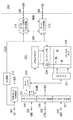
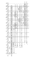
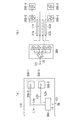
図1は、本発明の好ましい実施形態によるメモリモジュール100の構成を示す模式図である。
FIG. 1 is a schematic diagram showing a configuration of a
図1に示すように、本実施形態によるメモリモジュール100は、モジュール基板110と、モジュール基板110に搭載された複数のメモリチップ200、複数のデータレジスタバッファ300及び1個のコマンド/アドレス/コントロールレジスタバッファ400とを備えている。
As shown in FIG. 1, the
本実施形態では、メモリチップ200の搭載数は36個であり、各メモリチップを特に区別する必要があるときは、それぞれメモリチップ200−0〜200−35と表記する。また、本実施形態では、データレジスタバッファ300の搭載数は9個であり、各データレジスタバッファを特に区別する必要があるときは、それぞれデータレジスタバッファ300−0〜300−8と表記する。これに対し、コマンド/アドレス/コントロールレジスタバッファ400の搭載数は1個である。但し、本発明においてコマンド/アドレス/コントロールレジスタバッファ400の搭載数を1個とすることは必須でなく、2個以上のコマンド/アドレス/コントロールレジスタバッファ400を搭載しても構わない。
In the present embodiment, the number of mounted
モジュール基板110は多層配線が施されたプリント基板であり、その平面形状は、図1に示すX方向を長辺とし、Y方向を短辺とする略長方形である。モジュール基板110の一辺には、長辺であるX方向に沿って複数のデータコネクタ120及び複数のコマンド/アドレス/コントロールコネクタ130が設けられている。データコネクタ120及びコマンド/アドレス/コントロールコネクタ130は、後述するメモリスロットを介して、メモリコントローラとの電気的な接続を取るための端子である。
The
データコネクタ120は、メモリチップ200に書き込むべきライトデータ及びメモリチップ200から読み出されたリードデータを授受するためのコネクタである。特に限定されるものではないが、本実施形態ではデータコネクタ120のピン数は72個である。図1に示すように、これら72個のデータコネクタ120のうち、メモリチップ200−0〜200−19に対応するデータコネクタは、これらメモリチップ200−0〜200−19のほぼ真下に位置する領域110aに配置され、メモリチップ200−20〜200−35に対応するデータコネクタは、これらメモリチップ200−20〜200−35のほぼ真下に位置する領域110bに配置されている。
The
コマンド/アドレス/コントロールコネクタ130は、コマンド/アドレス/コントロールレジスタバッファ400に供給するコマンド信号、アドレス信号、コントロール信号及びクロック信号が供給されるコネクタである。図1に示すように、これらコマンド/アドレス/コントロールコネクタ130は、領域110aと領域110bとの間に位置する領域110cに配置されている。
The command / address /
メモリチップ200は例えばDRAMであり、枝番号が偶数であるメモリチップ200−0,200−2・・・はモジュール基板110の一方の表面に搭載され、枝番号が奇数であるメモリチップ200−1,200−3・・・はモジュール基板110の他方の表面に搭載されている。そして、対応する2個のメモリチップ、例えばメモリチップ200−0と200−1は、モジュール基板110を介して互いに対向する位置に搭載されている。
The
本実施形態によるメモリモジュール100は、いわゆる4Rank構成である。Rank数とは、排他的に選択されるメモリ空間の数を指す。各Rank間には同じアドレスが割り当てられるものの、チップセレクト(CS)信号を排他的に活性化させたり、クロックイネーブル(CKE)信号を排他的に活性化させたりすることによって、いずれか1つのRankが選択される。
The
本実施形態では、4個のメモリチップ200が一つの組を構成しており、これら4個のメモリチップ200が互いに異なるRankに属している。例えば、メモリチップ200−0〜200−3が一つの組を構成しており、これらメモリチップ200−0〜200−3が互い異なるRankに属している。
In the present embodiment, four
図1に示すように、このような組を構成する4個のメモリチップ200は、1つのデータレジスタバッファ300に接続されている。例えば、メモリチップ200−0〜200−3からなる組は、データレジスタバッファ300−0に接続されている。このうち、上側に搭載されたメモリチップ200−0,200−1は、データ配線L1を介してデータレジスタバッファ300−0に接続され、下側に搭載されたメモリチップ200−2,200−3は、データ配線L2を介してデータレジスタバッファ300−0に接続されている。尚、図1に示すデータ配線L1,L2の矢印は、いずれも1バイト(8ビット)分の配線を示している。データ配線L1,L2は、いずれもモジュール基板110の内部に形成された配線である。
As shown in FIG. 1, the four
メモリチップ200の動作は、コマンド/アドレス/コントロールレジスタバッファ400より供給されるコマンド信号、アドレス信号、コントロール信号及びクロック信号に基づいて制御される。メモリチップ200の詳細については後述する。
The operation of the
データレジスタバッファ300は、上述の通り、4個のメモリチップ200に対して1個ずつ割り当てられており、9個のデータレジスタバッファ300が長辺であるX方向に配列されている。データレジスタバッファ300は、データ配線L0を介して転送されるライトデータをバッファリングしてデータ配線L1,L2のいずれかへ出力するとともに、いずれかのデータ配線L1,L2を介して転送されるリードデータをバッファリングしてデータ配線L0に出力するためのチップである。データ配線L0も、モジュール基板110の内部に形成された配線である。
As described above, one
かかる構成により、1個のデータレジスタバッファ300と、これに対応するデータコネクタ120及び4個のメモリチップ200は、一つのグループGを構成している。同じグループに含まれるメモリチップ200、データレジスタバッファ300及びデータコネクタ120は、モジュール基板110の短辺であるY方向に並べて配置されており、このようなグループGが長辺であるX方向に並べて配置されている。したがって、各データレジスタバッファ300とこれに対応する4個のメモリチップ200との相対的な位置関係は、全てのグループGについて一定となる。
With this configuration, one
これにより、データ配線L0の配線長を短くすることができるとともに、グループ間におけるデータ配線L0の配線長をほぼ等しくすることが可能となる。同様に、データ配線L1,L2の配線長を短くすることができるとともに、グループ間におけるデータ配線L1,L2の配線長をほぼ等しくすることが可能となる。 As a result, the wiring length of the data wiring L0 can be shortened, and the wiring length of the data wiring L0 between the groups can be made substantially equal. Similarly, the wiring lengths of the data wirings L1, L2 can be shortened, and the wiring lengths of the data wirings L1, L2 between the groups can be made substantially equal.
データレジスタバッファ300の動作は、コマンド/アドレス/コントロールレジスタバッファ400より供給されるコントロール信号に基づいて制御される。データレジスタバッファ300の詳細については後述する。
The operation of the data register
コマンド/アドレス/コントロールレジスタバッファ400は、モジュール基板110に1個だけ搭載されている。図1に示すように、コマンド/アドレス/コントロールレジスタバッファ400は、モジュール基板110の長辺であるX方向における略中央部に配置されている。
Only one command / address /
コマンド/アドレス/コントロールレジスタバッファ400は、コマンド/アドレス/コントロールコネクタ130をから供給されるコマンド信号、アドレス信号、コントロール信号及びクロック信号(これらを纏めてコマンド/アドレス/コントロール信号と呼ぶことがある)を入力端子401で受け、これらをバッファリングしてメモリチップ200に供給するとともに、コントロール信号を生成する。メモリチップ200へ供給するコマンド/アドレス信号は、出力端子402を介して出力され、データバッファ300へ供給するコントロール信号は出力端子403を介して出力される。
The command / address /
出力端子402はコマンド/アドレス/コントロールレジスタバッファ400の左側用と右側用にそれぞれ1セット用意され、例えば左側の出力端子402は、Rankの選択などに必要なコントロール信号を除き、メモリチップ200−0〜200−19に対して共通接続されている。すなわち、コマンド信号、アドレス信号及びクロック信号は、メモリチップ200−0〜200−19に対して共通に供給される。また、出力端子403においても、コマンド/アドレス/コントロールレジスタバッファ400の左側用と右側用にそれぞれ1セット用意され、例えば左側の出力端子402は、データレジスタバッファ300−0〜300−4に対して共通接続されている。これにより、生成されたコントロール信号は、データレジスタバッファ300−0〜300−4に対して共通に供給される。
One set of
また、モジュール基板110には、コマンド/アドレス/コントロールレジスタバッファ400から出力されたコマンド/アドレス信号やコントロール信号の反射を防止すべく、X方向における端部に終端抵抗R1が設けられている。さらに、コマンド/アドレス/コントロールレジスタバッファ400に入力されるコマンド/アドレス/コントロール信号の反射波を吸収すべく、コマンド/アドレス/コントロールコネクタ130とコマンド/アドレス/コントロールレジスタバッファ400とを接続するコマンド/アドレス/コントロール配線L3の経路上には、スタブ抵抗R2が挿入されている。コマンド/アドレス/コントロールレジスタバッファ400の詳細については後述する。
Further, the
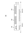
図2は、本実施形態によるメモリモジュール100を備える情報処理システム10の構成を示すブロック図である。
FIG. 2 is a block diagram illustrating a configuration of the
図2に示す情報処理システム10は、CPU11と、メモリコントロールハブ(MCH)12及びインターフェースコントロールハブ(ICH)13を介してCPU11に接続された各種デバイスとを備えている。
The
MCH12には、図1に示したメモリモジュール100及びグラフィックコントローラ15が接続されている。図2に示すように、メモリモジュール100とMCH12はメモリシステム20を構成し、MCH12はメモリモジュール100に対するコントローラ機能を有している。すなわち、メモリコントローラとして機能する。
The
ICH13には、ストレージデバイス16、I/Oデバイス17、及びBIOS(Basic Input/Output System)18が接続されている。ストレージデバイス16は、ハードディスクドライブなどの磁気ドライブや、CD−ROMドライブなどの光学ドライブなどが含まれる。また、I/Oデバイス17は、キーボード、マウスなどの入力デバイスや、スピーカなどの出力デバイス、さらには、モデム、LANなどのネットワークデバイスが含まれる。BIOS18は、当該情報処理システム10に関する基本的な各種情報を記憶する一種のファームウェアであり、フラッシュメモリなどの不揮発性メモリによって構成される。
A
図3は、メモリシステム20が形成された部分におけるマザーボードの構造を模式的に示す斜視図である。
FIG. 3 is a perspective view schematically showing the structure of the mother board in the portion where the
図3に示すように、マザーボード21にはメモリスロット22が設けられており、メモリスロット22にメモリモジュール100が挿入されている。一方、メモリコントローラ12は、マザーボード21に直接実装されている。既に説明したように、メモリモジュール100には複数のメモリチップ200が搭載されている。
As shown in FIG. 3, the
ここで、メモリコントローラ12とメモリチップ200との間の信号経路には、マザーボード21に形成された配線23と、モジュール基板110に形成されたデータ配線L0及びコマンド/アドレス/コントロール配線L3が存在する。しかしながら、図1を用いて説明したように、本実施形態によるメモリモジュール100では、データ配線L0にデータレジスタバッファ300が接続されているため、その先の信号経路に存在するメモリチップ200の負荷容量はメモリコントローラ12からは見えない。同様に、コマンド/アドレス/コントロール配線L3にはコマンド/アドレス/コントロールレジスタバッファ400が接続されているため、その先の信号経路に存在するメモリチップ200の負荷容量はメモリコントローラ12からは見えない。これにより、メモリコントローラ12とメモリモジュール100とを接続する信号経路の負荷容量が低減されるため、データ転送レートが高い場合であっても良好な信号品質を確保することが可能となる。
Here, in the signal path between the
尚、図3に示したメモリシステム20では、マザーボード21にメモリスロット22が1個だけ設けられているが、実際のメモリシステムでは、複数(例えば4個)のメモリスロットが設けられ、これらメモリスロットにそれぞれメモリモジュール100が装着される。複数のメモリモジュール100を装着すると信号経路の負荷容量はその分増大するが、本実施形態では、メモリモジュール1枚当たりの負荷容量が従来に比べて非常に小さいことから、複数のメモリモジュールを装着した場合であっても、高速なデータ転送を行うことが可能となる。
In the
次に、メモリチップ200の構成について説明する。
Next, the configuration of the
図4は、メモリチップ200の構成を示すブロック図である。
FIG. 4 is a block diagram showing a configuration of the
メモリチップ200はDRAMであり、図4に示すように、外部端子として、クロック端子201、コマンド端子202、コントロール端子206、アドレス端子203、データ入出力端子204及びデータストローブ端子205を備えている。このうち、クロック端子201、コマンド端子202及び、コントロール端子206、アドレス端子203については、図1に示したコマンド/アドレス/コントロール配線L5を介してコマンド/アドレスレジスタバッファ400に接続されている。また、データ入出力端子204及びデータストローブ端子205については、図1に示したデータ配線L1又はL2を介して、データレジスタバッファ300に接続されている。その他、電源端子なども備えられているが、これらについては図示を省略してある。
The
クロック端子201はクロック信号CKが供給される端子であり、供給されたクロック信号CKは、内部クロック生成回路211に供給される。内部クロック生成回路211の出力である内部クロックICLKは、各種内部回路に供給される。クロック信号CKはDLL回路212にも供給される。DLL回路212は、内部クロックLCLKを生成し、これをデータ入出力回路213及びデータストローブ信号入出力回路214に供給する役割を果たす。ここで、内部クロックLCLKは、クロック信号CKに対して位相制御された信号であり、リードデータDQ及びデータストローブ信号DQSの位相がクロック信号CKの位相と一致するよう、クロック信号CKに対してやや位相が進められている。
The
DLL回路212は、モードレジスタ215へのセット内容に応じて使用の可否が選択される。つまり、モードレジスタ215に「DLLオンモード」がセットされている場合には、DLL回路212は使用状態とされ、内部クロックLCLKはクロック信号CKに対して位相制御される。一方、モードレジスタ215に「DLLオフモード」がセットされている場合には、DLL回路212は不使用状態(クロック信号CKはショートカット)とされ、内部クロックLCLKはクロック信号CKに対して位相制御されなくなる。
Whether or not the
コマンド端子202は、ロウアドレスストローブ(RAS)信号、カラムアドレスストローブ(CAS)信号、ライトイネーブル(WE)信号などからなるコマンド信号CMDが供給される端子である。コントロール端子206は、チップセレクト(CS)信号、クロックイネーブル(CKE)信号、オンダイターミネーション(ODT)信号などの、Rankごとのコントロール信号CTRLが供給される端子である。チップセレクト(CS)信号により、コマンド発行対象となるDRAMが切り換えられ、DRAM内のクロック系の活性化や、オンダイターミネーション制御がなされる。コマンド信号CMDは、コマンドデコーダ216に供給される。コマンドデコーダ216は、内部クロックICLKに同期して、コマンド信号の保持、デコード及びカウントなどを行うことによって、各種内部コマンドICMDを生成する回路である。生成された内部コマンドは、モードレジスタ215を含む各種制御回路(図示せず)に供給される。また、コントロール信号CTRLは、コントロール回路218に供給される。コントロール回路218は、コントロール信号CTRLに基づいてODT信号などの内部コントロール信号を生成する回路である。
The
アドレス端子203は、アドレス信号ADDが供給される端子であり、供給されたアドレス信号ADDはアドレスラッチ回路217に供給される。アドレスラッチ回路217は、内部クロックICLKに同期してアドレス信号ADDをラッチする回路である。アドレスラッチ回路217にラッチされたアドレス信号ADDのうち、ロウアドレスについてはロウデコーダ221に供給され、カラムアドレスについてはカラムデコーダ222に供給される。また、モードレジスタセットにエントリしている場合には、アドレス信号ADDはモードレジスタ215に供給され、これによってモードレジスタ215の内容が更新される。
The
ロウデコーダ221は、メモリセルアレイ230に含まれるいずれかのワード線WLを選択する回路である。メモリセルアレイ230内においては、複数のワード線WLと複数のビット線BLが交差しており、その交点にはメモリセルMCが配置されている(図4では、1本のワード線WL、1本のビット線BL及び1個のメモリセルMCのみを示している)。ビット線BLは、センスアンプ列231に含まれるいずれかのセンスアンプSAに接続されている。センスアンプSAの選択は、カラムデコーダ222によって行われる。
The
選択されたセンスアンプSAは、データ入出力回路213に接続される。データ入出力回路213には、内部クロックLCLK及び内部データストローブ信号PDQSが供給されており、リード動作時においては内部クロックLCLKに同期してリードデータを出力し、ライト動作時においては内部データストローブ信号PDQSに同期してライトデータを取り込む。これにより、リード動作時においては、メモリセルアレイ230から読み出されたリードデータがデータ入出力端子204から出力され、ライト動作時においては、データ入出力端子204から受信したライトデータがメモリセルアレイ230に供給される。
The selected sense amplifier SA is connected to the data input /
データストローブ端子205は、データストローブ信号DQSの入出力を行うための端子であり、データストローブ信号入出力回路214に接続されている。データストローブ信号入出力回路214は、上述した内部データストローブ信号PDQSを生成し、これをデータ入出力回路213に供給する。
The
また、データ入出力回路213及びデータストローブ信号入出力回路214には、コントロール回路218の出力であるODT信号も供給されている。ODT信号が活性化すると、データ入出力回路213及びデータストローブ信号入出力回路214は、いずれも終端抵抗として機能する。
The data input /
以上がメモリチップ200の全体構成である。次に、データレジスタバッファ300の構成について説明する。
The above is the overall configuration of the
図5は、データレジスタバッファ300の構成を示すブロック図である。
FIG. 5 is a block diagram showing the configuration of the data register
図5に示すように、データレジスタバッファ300は、入出力端子340を介して供給されるデータDQを、入出力端子350を介して供給されるデータストローブ信号DQSでバッファリングするFIFO(Write)回路301と、入出力端子341又は342を介して供給されるデータDQを、入出力端子351又は352を介して供給されるデータストローブ信号DQSでバッファリングするFIFO(Read)回路302とを備えている。ストローブ生成回路376は、DLL回路310によって生成される内部クロックLCLKRに同期して、データコネクタ120へ供給すべきデータストローブ信号DQSを生成する。ストローブ生成回路374は、DLL回路310によって生成される内部クロックLCLKWに同期して、メモリチップ200へ供給すべきデータストローブ信号DQSを生成する。
As shown in FIG. 5, the data register
尚、図5に示すFIFO回路301,302は、1ビット分のデータの入出力を行う回路であり、実際には、入出力データ幅分のFIFO回路301,302を用意しておく。本実施形態では、1個のデータレジスタバッファ300が1バイト分のデータを入出力することから、8組のFIFO回路301,302が必要となる。
Note that the
入出力端子340,350はデータ配線L0を介してデータコネクタ120に接続される端子である。一方、入出力端子341,351はデータ配線L1を介してメモリチップ200に接続される端子であり、入出力端子342,352はデータ配線L2を介してメモリチップ200に接続される端子である。このように、データレジスタバッファ300は、メモリコントローラ12に接続される入出力端子の数(M個)と、メモリチップ200に接続される入出力端子の数(N個)の数が相違しており、本実施形態では、N=2Mである。換言すれば、データ配線L1,L2の数がデータ配線L0の数のN/M倍(本実施形態では2倍)とされている。
The input /
FIFO(Write)回路301の出力動作タイミングは、DLL回路310によって生成される内部クロックLCLKWによって規定される。FIFO(Read)回路302の出力動作タイミングは、DLL回路310によって生成される内部クロックLCLKRによって規定される。DLL回路310は、コマンド/アドレス/コントロールレジスタバッファ400より供給されるクロック信号CKに基づいて内部クロックLCLKWやLCLKRを生成する回路であり、メモリチップ200に設けられたDLL回路212と同様の回路構成及び機能を有している。DLL回路310の使用の可否については、データレジスタコントロール回路320の設定内容によって選択される。また、DLL回路310の代わりにPLL回路を用いても構わない。
The output operation timing of the FIFO (Write)
データレジスタコントロール回路320は、コマンド/アドレス/コントロールレジスタバッファ400より供給されるコントロール信号DRCに基づいて、データレジスタバッファ300の動作を制御する回路である。具体的には、バッファ制御信号BCを生成することにより、入力バッファINB及び出力バッファOUTBの動作を制御するとともに、選択信号SELを生成することにより、セレクタ331〜334の動作を制御する。出力バッファOUTBの制御内容としては、例えば出力インピーダンスの調整やODT動作のオンオフ制御が挙げられる。ODT機能の使用の可否は、モードレジスタ321の設定内容によって選択される。
The data register
また、データレジスタコントロール回路320は、フィードバック信号DRFを生成し、これをコマンド/アドレス/コントロールレジスタバッファ400に供給する。フィードバック信号DRFは、データレジスタバッファ300の現在のステータスを示す信号である。
The data register
さらに、データレジスタコントロール回路320には、ライトレベリング回路322及びリードレベリング回路323が含まれている。ライトレベリング回路322はライトレベリング動作を行うための回路であり、リードレベリング回路323はリードレベリング動作を行うための回路である。ライトレベリング動作及びリードレベリング動作については後述する。
Further, the data
セレクタ333は、FIFO(Write)回路301の出力であるデータDQを入出力端子341,342のいずれか一方に供給する回路である。また、セレクタ334は、入出力端子341,342から入力されたデータDQを選択し、選択したデータDQをFIFO(Read)回路302に供給する回路である。セレクタ331,332についても、それぞれセレクタ333,334と同様の機能を果たす。より具体的には、セレクタ332は、入出力端子351,352から入力されるデータストローブ信号DQSを選択する。選択されたデータストローブ信号DQSは、遅延回路372によりおおよそ90°位相を遅らせて、FIFO(Read)回路302に入力トリガ信号として供給される。セレクタ331は、ストローブ生成回路374から供給されるデータストローブ信号DQSを入出力端子351,352のいずれかに供給する。ストローブ生成回路374により生成されるデータストローブ信号DQSは、遅延回路370により内部クロックLCLKWよりもおおよそ90°位相が遅れる。これらセレクタ331〜334による上記の選択は、データレジスタコントロール回路320の出力である選択信号SELによって指定される。
The
このように、データレジスタバッファ300は、データ配線L0を介して転送されるライトデータをバッファリングしてデータ配線L1,L2のいずれかへ出力するとともに、いずれかのデータ配線L1,L2を介して転送されるリードデータをバッファリングしてデータ配線L0に出力する役割を果たす。ここで、データレジスタバッファ300はデータのバッファリングを行っているだけであることから、データ配線L0を介して転送されるライトデータ及びリードデータの転送レートと、データ配線L1,L2を介して転送されるライトデータ及びリードデータの転送レートとは互いに等しい。
As described above, the data register
このため、データレジスタバッファ300は、Fully Buffered型のメモリモジュールに用いられるAMBのような高価なチップではなく、比較的安価に提供されるチップを用いることが可能となる。
For this reason, the data register
以上がデータレジスタバッファ300の全体構成である。次に、コマンド/アドレス/コントロールレジスタバッファ400の構成について説明する。
The above is the overall configuration of the data register
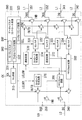
図6は、コマンド/アドレス/コントロールレジスタバッファ400の構成を示すブロック図である。
FIG. 6 is a block diagram showing the configuration of the command / address /
図6に示すように、コマンド/アドレス/コントロールレジスタバッファ400は、コマンド/アドレス/コントロールコネクタ130に接続される入力端子401と、メモリチップ200に接続される出力端子402と、データレジスタバッファ300に接続される出力端子403及び入力端子404とを備えている。
As shown in FIG. 6, the command / address /
入力端子401からは、メモリコントローラ12より供給されるコマンド/アドレス/コントロール信号が入力される。入力されたコマンド/アドレス/コントロール信号のうち、コマンド信号CMD、アドレス信号ADD及びコントロール信号CTRLについてはレジスタ回路410に供給され、クロック信号CKについてはPLL回路420に供給される。レジスタ回路410は、コマンド信号CMD、アドレス信号ADD及びコントロール信号CTRLをバッファリングする回路であり、バッファリングされたコマンド信号CMD、アドレス信号ADD及びコントロール信号CTRLは、出力端子402を介してメモリチップ200に供給される。
A command / address / control signal supplied from the
レジスタ回路410の動作タイミングは、PLL回路420によって生成される内部クロックLCLKCAによって規定される。PLL回路420は、メモリコントローラ12より供給されるクロック信号CKに基づいて内部クロックLCLKCAを生成する回路であり、メモリチップ200に設けられた回路212と同様の回路構成及び機能を有している。PLL回路420の使用の可否については、コントロール信号生成回路430に含まれるモードレジスタ431の設定内容によって選択される。また、PLL回路420の代わりにDLL回路を用いても構わない。
The operation timing of the
コントロール信号生成回路430は、入力端子401を介して供給されるコマンド/アドレス/コントロール信号に基づいて、データレジスタ300に供給するコントロール信号DRCを生成する回路であり、その動作は内部クロックLCLKCAに同期して行われる。データレジスタ300用のコントロール信号DRCは、出力端子403を介してデータレジスタバッファ300に供給される。また、データレジスタ300用のコントロール信号生成回路430には、入力端子404を介してデータレジスタバッファ300よりフィードバック信号DRFが供給される。
The control
コントロール信号DRCには、データの送受信方向を示す信号、データレジスタバッファ300のL0側のODTタイミングを制御する信号、L1、L2側のODTタイミングを制御する信号、DLL回路のオン/オフ制御をする信号、データレジスタバッファ300のイネーブル/ディセーブル制御をする信号、データレジスタバッファ300のモード切り替えおよびモードレジスタセットを行う信号などが含まれている。これらの信号には、それぞれ別個の配線を割り当てても構わないし、複数の信号に1本の配線を割り当てても構わない。また、これらの信号をコマンドとしてデータレジスタバッファ300に送信しても構わない。
The control signal DRC is a signal indicating a data transmission / reception direction, a signal for controlling the ODT timing on the L0 side of the data register
以上がコマンド/アドレス/コントロールレジスタバッファ400の全体構成である。
The overall configuration of the command / address /
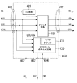
図7は、本実施形態によるメモリモジュール100の配線図である。
FIG. 7 is a wiring diagram of the
図7に示すように、本実施形態では、データコネクタ120とメモリチップ200との間にデータレジスタバッファ300が介在している。データコネクタ120とデータレジスタバッファ300はデータ配線L0によって接続され、データレジスタバッファ300とメモリチップ200はデータ配線L1又はL2によって接続されている。図7では、データ配線L0によって転送される複数のデータをDQ−Preと表記し、データ配線L1,L2によって転送されるデータをDQ−Postと表記している。同様に、データ配線L0によって転送されるデータストローブ信号をDQS−Preと表記し、データ配線L1,L2によって転送されるデータストローブ信号をDQS−Postと表記している。
As shown in FIG. 7, in this embodiment, a
データDQ−PreとデータDQ−Postの内容は同一であるが、データレジスタバッファ300によってバッファリングされる分、両者のタイミングにはずれが生じる。データストローブ信号DQS−Preとデータストローブ信号DQS−Postとの関係についても同様である。このため、本実施形態では、メモリチップ200とデータレジスタバッファ300との間のタイミング調整と、データレジスタバッファ300とメモリコントローラとの間のタイミング調整とは、それぞれ別個に行う必要がある。これらタイミング調整の具体的な方法については後述する。
The contents of the data DQ-Pre and the data DQ-Post are the same. The same applies to the relationship between the data strobe signal DQS-Pre and the data strobe signal DQS-Post. For this reason, in this embodiment, the timing adjustment between the
既に説明したとおり、本実施形態では、1個のデータレジスタバッファ300に4個のメモリチップ200が割り当てられている。これら4個のメモリチップ200は、互いに異なるRankを構成するメモリチップであり、コントロール信号CTRLに含まれるチップセレクト(CS)信号やクロックイネーブル(CKE)信号によって排他的に活性化される。アドレス/コマンド信号ADD,CMDについては、これら4個のメモリチップ200に対して共通に供給される。
As already described, in this embodiment, four
メモリチップ200に供給されるアドレス信号ADD、コマンド信号CMD、コントロール信号CTRL及びクロック信号CKは、コマンド/アドレス/コントロールレジスタバッファ400より供給される。また、データレジスタバッファ300に供給されるコントロール信号DRCについても、コマンド/アドレス/コントロールレジスタバッファ400より供給される。
The address signal ADD, command signal CMD, control signal CTRL, and clock signal CK supplied to the
図7に示すように、コマンド/アドレス/コントロールコネクタ130とコマンド/アドレス/コントロールレジスタバッファ400はコマンド/アドレス/コントロール配線L3によって接続され、コマンド/アドレス/コントロールレジスタバッファ400とデータレジスタバッファ300はコントロール配線L4によって接続され、コマンド/アドレス/コントロールレジスタバッファ400とメモリチップ200はコマンド/アドレス/コントロール配線L5によって接続されている。図7では、コマンド/アドレス/コントロール配線L3によって転送されるコマンド/アドレス信号をADD/CMD−Preと表記し、コマンド/アドレス/コントロール配線L5によって転送されるコマンド/アドレス信号をADD/CMD−Postと表記している。同様に、コマンド/アドレス/コントロール配線L3によって転送されるコントロール信号をCNTRL−Preと表記し、コマンド/アドレス/コントロール配線L5によって転送されるコントロール信号をCNTRL−Postと表記している。
As shown in FIG. 7, the command / address /
また、メモリチップ200及びデータレジスタバッファ300に供給されるクロック信号CKは、全てコマンド/アドレス/コントロールレジスタバッファ400より供給される。図7では、コマンド/アドレス/コントロール配線L3によって転送されるクロック信号をCK−Preと表記し、コントロール配線L4及びコマンド/アドレス/コントロール配線L5によって転送されるクロック信号をCK−Postと表記している。
The clock signals CK supplied to the
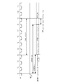
図8は、本実施形態によるメモリモジュールの1ビット分のデータ伝送経路を説明するための模式図であり、(a)はレイアウト図、(b)は配線図である。 FIG. 8 is a schematic diagram for explaining a data transmission path for one bit of the memory module according to the present embodiment, where (a) is a layout diagram and (b) is a wiring diagram.
図8(a),(b)に示すように、1ビットのデータはデータコネクタ120の所定のコネクタ121を介して授受される。コネクタ121は、1本のデータ配線L0を介してデータレジスタバッファ300に接続される。図5を用いて説明したように、本実施形態では、1本のデータ配線L0に対して2系統のデータ配線L1,L2が割り当てられている。具体的には、データ配線L1については2個のメモリチップ200−0,200−1に共通接続され、データ配線L2については2個のメモリチップ200−2,200−3に共通接続される。
As shown in FIGS. 8A and 8B, 1-bit data is exchanged via a
かかる構成により、1本のデータ配線L1又はL2の負荷容量が小さくなるとともに、分岐点の数が少なくなり、さらに、分岐点からの配線長も短くなることから、データ配線L1,L2上を伝送されるデータの信号品質が高められる。具体的には、1本のデータ配線L1に接続される端子は、メモリチップ200−0,200−1のデータ入出力端子と、データレジスタバッファ300のデータ出力端子の合計3端子だけである。しかも、図8(a)に示すように、メモリチップ200−0と200−1はモジュール基板110を介して互いに対向する搭載に配置されていることから、分岐点Pをメモリチップ200−0と200−1によって挟まれた領域に配置すれば、分岐点からメモリチップ200−0,200−1までの配線長が非常に短くなる。さらに、これらメモリチップ200−0〜200−3は互いに近接した位置に搭載されており、これによりメモリチップ間における遠近端差についても最小限に抑えられている。
With this configuration, the load capacity of one data line L1 or L2 is reduced, the number of branch points is reduced, and the length of the wiring from the branch point is also reduced, so that the data lines L1 and L2 are transmitted. The signal quality of the processed data is improved. Specifically, the terminals connected to one data line L1 are only a total of three terminals including the data input / output terminals of the memory chips 200-0 and 200-1 and the data output terminal of the data register
図9は、データ配線L1,L2を1本に纏めた場合における1ビット分のデータ伝送経路を説明するための模式図であり、(a)はレイアウト図、(b)は配線図である。 9A and 9B are schematic diagrams for explaining a data transmission path for one bit when the data wirings L1 and L2 are combined into one. FIG. 9A is a layout diagram, and FIG. 9B is a wiring diagram.
図9(a),(b)に示すように、データ配線L1,L2を1本に纏めた場合、データレジスタバッファ300と4個のメモリチップ200−0〜200−3が1本のデータ配線L1によって共通接続されることになる。このため、図8に示す構成と比べると、1本のデータ配線L1の負荷容量が大きくなるとともに、分岐点の数が多くなり、さらに、分岐点からの配線長も長くなる。具体的には、1本のデータ配線L1に接続される端子は、メモリチップ200−0〜200−3のデータ入出力端子と、データレジスタバッファ300のデータ出力端子の合計5端子となる。しかも、分岐点P1で2分岐し、分岐点P2にてさらに2分岐する構成となることから、分岐点P1からメモリチップ200−0〜200−3までの配線長が長くなる。
As shown in FIGS. 9A and 9B, when the data lines L1 and L2 are combined into one, the data register
これに対し、本実施形態においては、図8(a),(b)に示したように2系統のデータ配線L1,L2を用いていることから、モジュール基板内におけるデータの信号品質を高めることが可能となる。但し、2系統のデータ配線L1,L2を用いると、メモリチップ200とデータレジスタバッファ300とを接続する配線の本数が2倍に増加する。しかしながら、本実施形態では、図1を用いて説明したように、同じグループGを構成するメモリチップ200とデータレジスタバッファ300がモジュール基板110の短辺方向に並べて配置されていることから、配線スペースには十分な余裕がある。このため、短辺方向に延びる配線の本数が2倍に増えても問題なく配線を施すことが可能である。
On the other hand, in the present embodiment, as shown in FIGS. 8A and 8B, since the two data wirings L1 and L2 are used, the signal quality of data in the module board is improved. Is possible. However, when the two data lines L1 and L2 are used, the number of lines connecting the
一方、Fully Buffered型のメモリモジュールのように、モジュール基板の中央にデータを集中させるようなレイアウトである場合、モジュール基板の長辺方向に長いデータ配線を多数形成する必要がある。このようなレイアウトにおいては、本実施形態のレイアウトと比べてデータ配線の総延長が大幅に長くなるため、データ配線の本数を2倍とするためには、モジュール基板を構成する絶縁層の積層数を大幅に増やすなどの対策が必要となる。これに対し、本実施形態では上記の問題が生じないことから、モジュール基板110を構成する絶縁層の積層数を増やすことなく、メモリチップ200とデータレジスタバッファ300とを接続する配線本数を2倍とすることが可能となる。
On the other hand, when the layout is such that data is concentrated at the center of the module substrate, such as a fully buffered memory module, it is necessary to form a large number of long data wirings in the long side direction of the module substrate. In such a layout, the total length of the data wiring is significantly longer than in the layout of the present embodiment. Therefore, in order to double the number of data wirings, the number of insulating layers constituting the module substrate is increased. It is necessary to take measures such as significantly increasing On the other hand, since the above-described problem does not occur in the present embodiment, the number of wirings connecting the
図10は、2本のデータ配線L1,L2を用いたインターリーブ動作を説明するためのタイミング図である。 FIG. 10 is a timing chart for explaining an interleaving operation using two data lines L1 and L2.
図10はRank0〜Rank3からの連続したリード動作を示しており、バースト長が4ビット(BL=4)であるケース(或いは、バーストチョップによってバースト動作を4ビットで停止させたケース)を示している。図10に示す例では、クロック信号CKに同期した時刻T0,T2,T4,T6にてRank0,2,1,3の順にリードコマンドが発行されている。これらリードコマンドに応答して、所定のCASレイテンシ(本例ではCL=12)が経過した後、4ビットのリードデータDQがバースト出力される。
FIG. 10 shows a continuous read operation from
その結果、時刻T12〜T14の期間は、Rank0のメモリチップ200からデータ配線L1を用いたデータ転送が行われ、時刻T14〜T16の期間は、Rank2のメモリチップ200からデータ配線L2を用いたデータ転送が行われ、時刻T16〜T18の期間は、Rank1のメモリチップ200からデータ配線L1を用いたデータ転送が行われ、時刻T18〜T20の期間は、Rank3のメモリチップ200からデータ配線L2を用いたデータ転送が行われる。つまり、データ配線L1,L2が交互に使用される。
As a result, during the period from time T12 to T14, data transfer is performed using the data line L1 from the
このようにして次々と転送されるリードデータは、データレジスタバッファ300に供給され、データレジスタバッファ300に含まれるFIFO回路によってバッファリングされた後、データ配線L0へ出力される。図10に示す例では、データレジスタバッファ300にリードデータが入力されてから、1クロックサイクル遅れてリードデータが出力されている。
The read data successively transferred in this way is supplied to the data register
このように、本実施形態では、2本のデータ配線L1,L2を用いたインターリーブ動作が可能であることから、複数のメモリチップに対するリード動作を途切れることなく連続的に実行することが可能となる。これにより、データレジスタバッファ300から出力されるリードデータも途切れることなくメモリコントローラへ供給することができ、バスの利用効率を高めることが可能となる。尚、本実施形態においてデータ配線L1とL2が同時に使用されることはないが、これらデータ配線L1,L2を1本に纏めると、異なるメモリチップから出力されるリードデータ間に1クロックサイクル以上の時間を空ける必要が生じる。これに対し、本実施形態では、2本のデータ配線L1,L2を交互に使用していることから、異なるメモリチップから出力されるリードデータ間に隙間を設ける必要が無い。
As described above, in this embodiment, since the interleave operation using the two data wirings L1 and L2 is possible, the read operation for a plurality of memory chips can be continuously executed without interruption. . As a result, the read data output from the data register
尚、図10においてはリード動作を例に説明したが、ライト動作についても同様のインターリーブ動作が可能である。 Although the read operation is described as an example in FIG. 10, a similar interleave operation is possible for the write operation.
以下、本実施形態によるメモリモジュール100の動作について、より詳細に説明する。
Hereinafter, the operation of the
図11は、本実施形態によるメモリモジュール100のリード動作を説明するためのタイミング図である。
FIG. 11 is a timing diagram for explaining a read operation of the
リード動作においては、メモリコントローラ12からアクティブコマンドACT及びリードコマンドreadがこの順に発行される。図11に示す例では、クロック信号CKに同期した時刻T−5にてアクティブコマンドACTがコマンド/アドレス/コントロールコネクタ130に到達し、時刻T0にてリードコマンドreadがコマンド/アドレス/コントロールコネクタ130に到達している。
In the read operation, the active command ACT and the read command read are issued in this order from the
コマンド/アドレス/コントロールコネクタ130に到達したこれらコマンドACT,readは、コマンド/アドレス/コントロールレジスタバッファ400に入力される。ここで、これらコマンドACT,readがコマンド/アドレス/コントロールコネクタ130に到達するタイミングと、これらコマンドACT,readがコマンド/アドレス/コントロールレジスタバッファ400に入力されるタイミングとの間には所定の時間差(Flight Time)が生じる。
The commands ACT and read that have arrived at the command / address /
コマンド/アドレス/コントロールレジスタバッファ400は、受信したコマンドACT,readを図6に示したレジスタ回路410にて、入力クロック信号によってレジスタリングした後、メモリチップ200に出力する。この時、クロック信号CK出力については追加の1/2クロックサイクル相当量の遅延を持たせることにより、コマンドACT,read出力との同期を図る。また、コマンド/アドレス/コントロールレジスタバッファ400は、リードコマンドReadをコントロール信号DRCの一部としてデータレジスタバッファ300にも供給する。
The command / address /
そして、メモリチップ200はコマンドACT,readを受け、実際にリード動作を開始する。ここで、コマンドACT,readがコマンド/アドレス/コントロールレジスタバッファ400から出力されるタイミングと、コマンドACT,readがメモリチップ200に入力されるタイミングとの間には所定の時間差(Flight Time)が生じる。
The
図11に示す例ではCL=5に設定されていることから、メモリチップ200はリードコマンドreadを受けてから5クロックサイクル後である時刻T5からリードデータDQのバースト出力を開始する。図11に示す例では、バースト長は8ビット(BL=8)である。メモリチップ200からバースト出力されるリードデータDQ及びデータストローブ信号DQSは、データレジスタバッファ300に供給される。
In the example shown in FIG. 11, since CL = 5 is set, the
データレジスタバッファ300は、メモリチップ200から出力されるリードデータDQを、一定位相量(たとえば、おおむね、90°の位相差分)だけ遅延させたデータストローブ信号DQSでFIFO回路302に取り込む。ここで、リードデータDQ及びデータストローブ信号DQSがメモリチップ200から出力されるタイミングと、リードデータDQ及びデータストローブ信号DQSがデータレジスタバッファ300に入力されるタイミングとの間には所定の時間差(Flight Time)が生じる。
The data register
そして、データレジスタバッファ300は、FIFO回路302を用いて内部クロックLCLKRに同期したリタイミングを行い、CL=6に変換して出力する。これにより、メモリコントローラは、正しくリードデータを受信することが可能となる。
The data register
以上が本実施形態によるメモリモジュール100のリード動作である。次に、ライト動作について説明する。
The above is the read operation of the
図12は、本実施形態によるメモリモジュール100のライト動作を説明するためのタイミング図である。
FIG. 12 is a timing chart for explaining the write operation of the
ライト動作においては、メモリコントローラからアクティブコマンドACT及びライトコマンドWriteがこの順に発行されるとともに、ライトコマンドWriteを発行してからライトレイテンシ(WL)が経過した後、ライトデータをバースト出力する。図12に示す例では、クロック信号CKに同期した時刻T−5にてアクティブコマンドACTがコマンド/アドレス/コントロールコネクタ130に到達し、時刻T0にてライトコマンドWriteがコマンド/アドレス/コントロールコネクタ130に到達している。また、本例ではWL=4に設定されており、データコネクタ120には時刻T4からライトデータが入力される。
In the write operation, the active command ACT and the write command Write are issued in this order from the memory controller, and after the write latency (WL) has elapsed since the write command Write is issued, the write data is burst output. In the example shown in FIG. 12, the active command ACT reaches the command / address /
コマンドの流れは図11に示したリード動作と同様であることから、重複する説明は省略する。一方、データコネクタ120に到達したこれらライトデータDQは、データレジスタバッファ300に入力される。ここで、ライトコマンドがコマンド/アドレス/コントロールコネクタ130に到達するタイミングと、ライトコマンド(Direction Control)がデータレジスタバッファ300に入力されるタイミングとの間には所定の時間差(Flight Time)が生じる。これを考慮して、メモリコントローラは、このFlight Time分だけ遅れてライトデータDQを出力する。
Since the flow of commands is the same as that of the read operation shown in FIG. On the other hand, the write data DQ reaching the
データレジスタバッファ300は、受け付けたライトデータDQを、一定位相量(たとえば、おおむね、90°の位相差分)だけ遅延させたデータストローブ信号DQSでFIFO回路301に取り込む。そして、データレジスタバッファ300は、FIFO回路301を用いて内部クロックLCLKWに同期したリタイミングを行い、WL=5に変換して出力する。既に説明したとおり、データレジスタバッファ300からメモリチップ200へのライトデータの送信は、2本のデータ配線L1,L2のいずれか一方を用いて行われる。いずれのデータ配線を用いるかは、指定されたRankによって決まる。
The data register
そして、メモリチップ200は、データレジスタバッファ300からバースト出力されるライトデータDQを受信し、これをメモリセルアレイに書き込む。ここで、ライトデータDQ及びデータストローブ信号DQSがデータレジスタバッファ300から出力されるタイミングと、ライトデータDQ及びデータストローブ信号DQSがメモリチップ200に入力されるタイミングとの間には所定の時間差(Flight Time)が生じる。これを考慮して、データレジスタバッファ300は、このFlight Time分だけ早くライトデータDQを出力する。これにより、メモリチップ200は正しくライトデータDQを受信することが可能となる。
Then, the
次に、本実施形態によるメモリモジュール100の起動時における初期化動作について説明する。
Next, the initialization operation at the time of starting the
図13は、メモリモジュール100の起動時における初期化動作を説明するためのフローチャートである。
FIG. 13 is a flowchart for explaining an initialization operation when the
まず、電源が投入されると(ステップS1)、メモリチップ200、データレジスタバッファ300及びコマンド/アドレス/コントロールレジスタバッファ400は、それぞれ内部でリセット信号を活性化し、内部回路をリセットする(ステップS2)。これにより、メモリチップ200、データレジスタバッファ300及びコマンド/アドレス/コントロールレジスタバッファ400は、それぞれ初期化動作を実行する。初期化動作にはモードレジスタの設定動作が含まれており、これにより、メモリチップ200、データレジスタバッファ300及びコマンド/アドレス/コントロールレジスタバッファ400にそれぞれ含まれるモードレジスタ215,321,431に所定のモード情報が設定される(ステップS3)。
First, when the power is turned on (step S1), the
モードレジスタに対する設定動作が完了すると、次に、データレジスタバッファ300とメモリチップ200との間のレベリング動作が行われる(ステップS4)。レベリング動作とは、信号の伝搬時間を考慮してライトタイミングやリードのタイミングを調整する動作である。ライトタイミングの調整はライトレベリング動作によって行われ、リードタイミングの調整はリードレベリング動作によって行われる。
When the setting operation for the mode register is completed, a leveling operation is performed between the data register
データレジスタバッファ300とメモリチップ200との間のレベリング動作が完了すると、次に、メモリコントローラとデータレジスタバッファ300との間のレベリング動作が行われる(ステップS5)。
When the leveling operation between the data register
図14は、データレジスタバッファ300とメモリチップ200との間のライトレベリング動作を説明するためのタイミング図であり、(a)はレベリング開始時におけるタイミング図、(b)レベリング終了時におけるタイミング図である。この動作は、図5に示したライトレベリング回路322によって行われる。
FIG. 14 is a timing diagram for explaining a write leveling operation between the data register
データレジスタバッファ300とメモリチップ200との間のライトレベリング動作においては、まず、図14(a)に示すように、データレジスタバッファ300からクロック信号CKに同期したデータストローブ信号DQSを出力する。クロック信号CKはコマンド/アドレス/コントロールレジスタバッファ400から供給される信号であり、既に説明したとおり、メモリチップ200にも供給される。ここで、データストローブ信号DQSがメモリチップ200に伝達されるまでにはある程度の伝搬時間が必要であることから、メモリチップ200側においては、クロック信号CKとデータストローブ信号DQSの入力タイミングは必ずしも一致しない。
In the write leveling operation between the data register
図14(a)に示す例では、メモリチップ200側において、データストローブ信号DQSの立ち上がりエッジにおけるクロック信号CKの論理レベルが「ハイレベル」であるケースを示している。これに応答して、メモリチップ200はデータ入出力端子204から「ハイレベル」の信号DQを出力する。かかる信号DQは、データレジスタバッファ300に入力され、これにより、データレジスタバッファ300は、クロック信号CKとデータストローブ信号DQSの位相がどの方向にずれているのかを知ることができる。
The example shown in FIG. 14A shows a case where the logic level of the clock signal CK at the rising edge of the data strobe signal DQS is “high” on the
データレジスタバッファ300のライトレベリング回路322は、位相のズレ方向に基づいてLCLKWを変位させ、データストローブ信号DQSの出力タイミングを変化させる。図14(a)に示す例では、メモリチップ200に到達するクロック信号CKの立ち上がりエッジに比べて、データストローブ信号DQSの到達が遅れていることから、データレジスタバッファ300は、データストローブ信号DQSの出力タイミングを早める。
The
そして、上記の動作を繰り返すと、図14(b)に示すように、メモリチップ200側において、データストローブ信号DQSの立ち上がりエッジにおけるクロック信号CKの論理レベルが「ローレベル」に変化する。これによりライトレベリング動作が終了し、データレジスタバッファ300は、入力されるクロック信号CKを基準として、データストローブ信号DQSの出力すべきタイミングを知ることができる。ライトレベリング動作の結果は、データレジスタバッファ300内のデータレジスタコントロール回路320に記憶される。このようにしてライトレベリング動作が完了すると、メモリチップ200に入力されるクロック信号CKとデータストローブ信号DQSの位相は実質的に一致することになる。
When the above operation is repeated, as shown in FIG. 14B, the logic level of the clock signal CK at the rising edge of the data strobe signal DQS changes to “low level” on the
図15は、データレジスタバッファ300とメモリチップ200との間のリードレベリング動作を説明するためのタイミング図である。この動作は、図5に示したリードレベリング回路323によって行われる。
FIG. 15 is a timing diagram for explaining a read leveling operation between the data register
データレジスタバッファ300とメモリチップ200との間のリードレベリング動作においては、図15に示すように、コマンド/アドレス/コントロールレジスタバッファ400からクロック信号CKを出力するとともに、アクティブコマンドACT及びリードコマンドReadを発行する。クロック信号CKはメモリチップ200及びデータレジスタバッファ300に供給され、コマンドACT,readはメモリチップ200に供給される。また、リードコマンドReadについては、コントロール信号DRCの一部としてデータレジスタバッファ300にも供給される。
In the read leveling operation between the data register
図15に示す例では、クロック信号CKに同期した時刻T−5にてアクティブコマンドACTが発行され、時刻T0にてリードコマンドReadが発行されている。つまり、RAS−CASディレイ(tRCD)は5クロックサイクルである。 In the example shown in FIG. 15, the active command ACT is issued at time T-5 synchronized with the clock signal CK, and the read command Read is issued at time T0. That is, the RAS-CAS delay (tRCD) is 5 clock cycles.
メモリチップ200は、リードコマンドReadを受けて実際にリード動作を実行する。図15に示す例では、CASレイテンシが5クロックサイクル(CL=5)に設定されており、したがって、時刻T5からリードデータDQの出力が開始される。リードレベリング時におけるリードデータDQは、たとえば、ハイレベルとローレベルが交互に繰り返される信号などである。
The
メモリチップ200から出力されたリードデータDQは、データレジスタバッファ300に到達し、これにより、データレジスタバッファ300は、コントロール信号DRCの一部として入力されたリードコマンドReadの入力タイミングから、リードデータDQが入力されるまでの時間Aを知ることができる。かかる時間はメモリチップ200ごとに測定され、データレジスタバッファ300内のデータレジスタコントロール回路320に記憶され、入力バッファ回路INBの活性化タイミングの調整等に使われる。図15には、リードコマンドReadの入力からリードデータDQの入力までの時間Aが短いケース(メモリチップ200−0とデータレジスタバッファ300−0との間)と、長いケース(メモリチップ200−19とデータレジスタバッファ300−4との間)の2つを示している。
The read data DQ output from the
図16は、メモリコントローラ12とデータレジスタバッファ300との間のライトレベリング動作を説明するためのタイミング図であり、(a)はレベリング開始時におけるタイミング図、(b)レベリング終了時におけるタイミング図である。この動作は、図2に示したライトレベリング回路12aによって行われる。
FIG. 16 is a timing chart for explaining the write leveling operation between the
メモリコントローラ12とデータレジスタバッファ300との間のライトレベリング動作においては、まず、図16(a)に示すように、メモリコントローラ12からクロック信号CKとデータストローブ信号DQSを出力する。このうち、クロック信号CKについてはコマンド/アドレス/コントロールレジスタバッファ400を介してデータレジスタバッファ300に供給され、データストローブ信号DQSについてはデータレジスタバッファ300に直接供給される。したがって、データレジスタバッファ300側においては、クロック信号CKとデータストローブ信号DQSの入力タイミングは必ずしも一致しない。
In the write leveling operation between the
図16(a)に示す例では、データレジスタバッファ300側において、データストローブ信号DQSの立ち上がりエッジにおけるクロック信号CKの論理レベルが「ローレベル」であるケースを示している。これに応答して、データレジスタバッファ300は入出力端子340から「ローレベル」の信号DQを出力する。かかる信号DQは、メモリコントローラ12に供給され、これにより、メモリコントローラ12はクロック信号CKとデータストローブ信号DQSの位相がどの方向にずれているのかを知ることができる。
The example shown in FIG. 16A shows a case where the logic level of the clock signal CK at the rising edge of the data strobe signal DQS is “low level” on the data register
メモリコントローラ12は、位相のズレ方向に基づいてデータストローブ信号DQSの出力タイミングを変化させる。図16(a)に示す例では、データレジスタバッファ300に到達するクロック信号CKの立ち上がりエッジに比べて、データストローブ信号DQSの到達が進んでいることから、メモリコントローラ12は、データストローブ信号DQSの出力タイミングを遅らせる。
The
そして、上記の動作を繰り返すと、図16(b)に示すように、データレジスタバッファ300側において、データストローブ信号DQSの立ち上がりエッジにおけるクロック信号CKの論理レベルが「ハイレベル」に変化する。これによりライトレベリング動作が終了し、メモリコントローラ12は、自ら出力するクロック信号CKを基準として、データストローブ信号DQSの出力すべきタイミングを知ることができる。ライトレベリング動作の結果は、メモリコントローラ12の内部回路に記憶される。このようにしてライトレベリング動作が完了すると、データレジスタバッファ300に入力されるクロック信号CKとデータストローブ信号DQSの位相は実質的に一致することになる。
When the above operation is repeated, as shown in FIG. 16B, the logic level of the clock signal CK at the rising edge of the data strobe signal DQS changes to “high level” on the data register
図17は、メモリコントローラ12とデータレジスタバッファ300との間のリードレベリング動作を説明するためのタイミング図である。この動作は、図2に示したリードレベリング回路12bによって行われる。
FIG. 17 is a timing chart for explaining a read leveling operation between the
メモリコントローラ12とデータレジスタバッファ300との間のリードレベリング動作においては、図17に示すように、メモリコントローラ12からクロック信号CKを出力するとともに、アクティブコマンドACT及びリードコマンドReadを発行する。クロック信号CKはデータレジスタバッファ300に供給され、コマンドACT,readは、コマンド/アドレス/コントロールレジスタバッファ400を介し、コントロール信号DRCの一部としてデータレジスタバッファ300に供給される。
In the read leveling operation between the
図17に示す例では、クロック信号CKに同期した時刻T−5にてアクティブコマンドACTが発行され、時刻T0にてリードコマンドReadが発行されている。つまり、RAS−CASディレイ(tRCD)は5クロックサイクルである。 In the example shown in FIG. 17, the active command ACT is issued at time T-5 synchronized with the clock signal CK, and the read command Read is issued at time T0. That is, the RAS-CAS delay (tRCD) is 5 clock cycles.
データレジスタバッファ300は、リードコマンドReadを受けて、あらかじめ定められたCASレイテンシが経過した後、ダミーデータDQを出力する。ダミーデータDQは、メモリチップ200から読み出されたリードデータではなく、データレジスタバッファ300内のデータレジスタコントロール回路320によって自動生成されたデータである。図17に示す例では、CASレイテンシが6クロックサイクル(CL=6)に設定されており、したがって、時刻T6からダミーデータDQの出力が開始される。ダミーデータDQは、たとえば、ハイレベルとローレベルが交互に繰り返される信号などである。
The data register
データレジスタバッファ300から出力されたダミーデータDQは、メモリコントローラ12に到達し、これにより、メモリコントローラ12はリードコマンドReadの発行タイミングから、リードデータDQが入力されるまでの時間Bを知ることができる。かかる時間はデータレジスタバッファ300ごとに測定され、メモリコントローラ12の内部回路に記憶され、入力バッファ回路(図示せず)の活性化タイミングの調整等に使われる。図17には、リードコマンドReadの発行からリードデータDQの入力までの時間Bが短いケース(メモリコントローラ12とデータレジスタバッファ300−0との間)と、長いケース(メモリコントローラ12とデータレジスタバッファ300−4との間)の2つを示している。
The dummy data DQ output from the data register
以上が本実施形態によるメモリモジュール100の起動時における初期化動作である。次に、本発明によるメモリモジュール100とDLL回路及びODT機能との関係について説明する。
The above is the initialization operation when starting the
既に説明したように、DLL回路とは、外部クロック信号に対して位相制御された内部クロック信号を生成する回路であり、リードデータDQ及びデータストローブ信号DQSの位相をクロック信号CKの位相と一致させるために用いられる。DDR3型のDRAMのような近年の高速メモリにおいては、DLL回路の使用はほぼ必須であり、DLL回路を使用しなければ正常なデータ転送を行うことが困難となる。その一方で、DLL回路は消費電力が比較的大きいという問題を有している。 As already described, the DLL circuit is a circuit that generates an internal clock signal whose phase is controlled with respect to the external clock signal, and makes the phases of the read data DQ and the data strobe signal DQS coincide with the phase of the clock signal CK. Used for. In a recent high-speed memory such as a DDR3 type DRAM, the use of a DLL circuit is almost indispensable, and it is difficult to perform normal data transfer without using a DLL circuit. On the other hand, the DLL circuit has a problem that power consumption is relatively large.
一方、ODT機能とは、終端抵抗をメモリチップの内部に持たせる機能であり、反射による信号品質の劣化を防止するために用いられる。通常のメモリモジュールは、1本のデータ配線に多数のメモリチップが共通接続されることから、近年の高速メモリにおいては、ODT機能の使用はほぼ必須であり、ODT機能をオフにすると信号波形が著しく劣化する。その一方で、ODT機能をオンにすると、消費電力が増大するという問題を有している。また、ODT動作は、データの入出力動作と同期している必要があるため、基本的に、DLL回路の使用が前提となる。 On the other hand, the ODT function is a function of providing a termination resistor inside the memory chip, and is used to prevent signal quality deterioration due to reflection. In a normal memory module, since a large number of memory chips are commonly connected to one data wiring, the use of the ODT function is almost indispensable in recent high-speed memories. When the ODT function is turned off, a signal waveform is generated. Deteriorates significantly. On the other hand, when the ODT function is turned on, there is a problem that power consumption increases. In addition, since the ODT operation needs to be synchronized with the data input / output operation, it is basically assumed that a DLL circuit is used.
図18は、DLL回路を使用せずにODT動作を行う場合の問題点を説明するためのタイミング図である。 FIG. 18 is a timing chart for explaining a problem when the ODT operation is performed without using the DLL circuit.
図18に示す例では、時刻T0の直前にODT信号をアクティブに変化させている。これに応答して、メモリチップ200の内部回路は、時刻T0のクロック信号CKに同期してODT機能をオンさせる。しかしながら、ODTインピーダンス(データ入出力端子204,205のインピーダンス)は直ちに所望の値とはならず、tAONDFminが経過しないとハイインピーダンス状態(RTT_OFF)から変化しない。本例では、tAONDFminは約3クロックサイクルである。
In the example shown in FIG. 18, the ODT signal is actively changed immediately before time T0. In response to this, the internal circuit of the
tAONDFminが経過した後は、電源電圧やチップ温度の条件次第でハイインピーダンス状態ではなくなるが、条件によってはまだ所望のインピーダンスRTT_ONにはならない。最悪の条件下では、所望のインピーダンスRTT_ONが得られるのは、時刻T0からtAONDFmaxが経過した後であり、本例ではtAONDFmaxは約8クロックサイクルである。 After tAONDFmin elapses, the high impedance state is lost depending on the conditions of the power supply voltage and the chip temperature, but the desired impedance RTT_ON is not yet achieved depending on the conditions. Under the worst conditions, the desired impedance RTT_ON is obtained after tAONDFmax has elapsed since time T0, and in this example tAONDFmax is about 8 clock cycles.
したがって、ODTインピーダンスが不定状態となる時刻T3から、ODTインピーダンスが所望の値RTTとなる次のサイクルである時刻T9までの期間は、インピーダンスが不定な期間である。このため、この期間は他のメモリチップにアクセスできないロスサイクルとなる。このように、DLL回路を使用せずにODT動作を行うと、ODT機能のオン/オフの切り替えが非同期となることから、インピーダンスの不定期間が長くなり、その間のリードライト動作が妨げられる。 Therefore, the period from time T3 when the ODT impedance becomes indefinite to time T9, which is the next cycle when the ODT impedance becomes the desired value RTT, is a period where the impedance is undefined. For this reason, this period is a loss cycle in which other memory chips cannot be accessed. As described above, when the ODT operation is performed without using the DLL circuit, the on / off switching of the ODT function becomes asynchronous, so that the indefinite period of impedance becomes long, and the read / write operation during that period is hindered.
このようなロスサイクルの問題を考慮すれば、DLL回路を使用しない場合にはODT機能も使用しないことが望ましいが、上述の通り、通常のメモリモジュールにおいてODT機能はほぼ必須であり、これをオフにすることは困難である。 Considering such a loss cycle problem, it is desirable not to use the ODT function when the DLL circuit is not used. However, as described above, the ODT function is almost essential in a normal memory module. It is difficult to make.
しかしながら、本実施形態によるメモリモジュール100では、メモリチップ200に接続されたデータ配線L1,L2の負荷容量が非常に小さいことから、DDR3型のDRAMのような高速メモリを用いた場合であっても、ODT動作をオフ状態で使用することができる。しかも、メモリチップ200とデータレジスタバッファ300との距離が非常に短いことから、DLL回路を用いた同期制御を行わなくても、正しくデータ転送を行うことができる。すなわち、ODT機能及びDLL回路ともオフ状態とすることができるので、消費電力を大幅に低減することが可能となる。さらには、メモリチップ200からODT回路及びDLL回路を排除することもでき、この場合には、チップ面積を縮小することも可能となる。
However, in the
次に、ODT機能及びDLL回路の使用の有無による動作タイミングの違いについて説明する。 Next, a difference in operation timing depending on whether the ODT function and the DLL circuit are used will be described.
図19は、ODT機能及びDLL回路ともオン状態とした場合のリードtoリード動作を説明するためのタイミング図である。 FIG. 19 is a timing chart for explaining a read-to-read operation when both the ODT function and the DLL circuit are turned on.
図19に示すように、ODT機能及びDLL回路ともオン状態でのリード動作タイミングは、図11に示した動作タイミングと基本的に同じである。図19に示す例では、時刻T0においてRank0に対してリードコマンドReadが発行され、時刻T6においてRank1に対してリードコマンドReadが発行されている。Rank0のメモリチップ200とRank1のメモリチップ200は、データ配線L1に共通接続されているため、相互に影響を及ぼし合う。
As shown in FIG. 19, the read operation timing in the ON state of both the ODT function and the DLL circuit is basically the same as the operation timing shown in FIG. In the example shown in FIG. 19, a read command Read is issued to Rank0 at time T0, and a read command Read is issued to Rank1 at time T6. Since the
このため、Rank0のメモリチップ200からリードデータDQがバースト出力される時刻T5〜T9の期間においては、Rank1のメモリチップ200のデータ入出力端子204は、ODT機能によってインピーダンスがRtt_Nomに設定される。同様に、Rank1のメモリチップ200からリードデータDQがバースト出力される時刻T11〜T15の期間においては、Rank0のメモリチップ200のデータ入出力端子204は、ODT機能によってインピーダンスがRtt_Nomに設定される。
For this reason, during the period from time T5 to T9 when the read data DQ is burst output from the
このように、一方のメモリチップ200がリードデータDQを出力している間は、他方のメモリチップ200がODT動作を行うため、信号の反射が防止される。但し、上述の通り、DLL回路及びODT機能の使用による消費電流が発生する。
In this way, while one
図20は、ODT機能及びDLL回路ともオフ状態とした場合のリードtoリード動作を説明するためのタイミング図である。 FIG. 20 is a timing chart for explaining a read-to-read operation when both the ODT function and the DLL circuit are turned off.
図20に示すように、DLL回路をオフ状態とすると、リードデータDQの出力タイミングはクロック信号CKに対して非同期となる。しかしながら、本実施形態では、メモリチップ200とデータレジスタバッファ300との距離が非常に近いことから、データレジスタバッファ300は非同期に出力されたリードデータDQを正しく受信することが可能である。また、Rank0のメモリチップとRank1のメモリチップは、データ配線L1のほぼ末端に配置されていることから、非動作側のメモリチップ200による信号の反射の影響も非常に少ない。このようにして非同期に出力されたリードデータDQは、データレジスタバッファ300においてリタイミングされ、メモリコントローラ12へ出力される。
As shown in FIG. 20, when the DLL circuit is turned off, the output timing of the read data DQ is asynchronous with respect to the clock signal CK. However, in this embodiment, since the distance between the
このように、本実施形態においては、メモリチップ200のODT機能及びDLL回路をいずれもオフ状態にした場合であっても、これらをオン状態とした場合と同様のリード動作を行うことが可能となる。むしろ、DLL回路によるタイミング調整が行われない分、リードデータDQの出力タイミングが早くなるため、より高速なアクセスが実現できる可能性がある。
Thus, in this embodiment, even when both the ODT function and the DLL circuit of the
図21は、ODT機能及びDLL回路ともオン状態とした場合のライトtoライト動作を説明するためのタイミング図である。 FIG. 21 is a timing chart for explaining the write-to-write operation when both the ODT function and the DLL circuit are turned on.
図21に示すように、ODT機能及びDLL回路ともオン状態でのライト動作タイミングは、図12に示した動作タイミングと基本的に同じである。図21に示す例では、時刻T0においてRank0に対してライトコマンドWriteが発行され、時刻T6においてRank1に対してライトコマンドWriteが発行されている。上述の通り、Rank0のメモリチップ200とRank1のメモリチップ200は、データ配線L1に共通接続されているため、相互に影響を及ぼし合う。
As shown in FIG. 21, the write operation timing in the ON state of both the ODT function and the DLL circuit is basically the same as the operation timing shown in FIG. In the example shown in FIG. 21, a write command Write is issued to Rank0 at time T0, and a write command Write is issued to Rank1 at time T6. As described above, the
このため、Rank0のメモリチップ200へライトデータDQがバースト入力される時刻T5〜T9の期間においては、Rank1のメモリチップ200のデータ入出力端子204は、ODT機能によってインピーダンスがRtt_Nomに設定される。同様に、Rank1のメモリチップ200へライトデータDQがバースト入力される時刻T11〜T15の期間においては、Rank0のメモリチップ200のデータ入出力端子204は、ODT機能によってインピーダンスがRtt_Nomに設定される。
Therefore, during the period from time T5 to time T9 when the write data DQ is burst input to the
このように、一方のメモリチップ200がライトデータDQを受け付けている間は、他方のメモリチップ200がODT動作を行うため、信号の反射が防止される。但し、上述の通り、DLL回路及びODT機能の使用による消費電流が発生する。
In this way, while one
図22は、ODT機能及びDLL回路ともオフ状態とした場合のライトtoライト動作を説明するためのタイミング図である。 FIG. 22 is a timing chart for explaining the write-to-write operation when both the ODT function and the DLL circuit are turned off.
図22に示すように、ODT機能をオフにすると、非動作側のメモリチップ200のデータ入出力端子204はハイインピーダンス状態となり、ここで信号の反射が生じる。しかしながら、本実施形態では、メモリチップ200とデータレジスタバッファ300との距離が非常に近く、且つ、Rank0のメモリチップとRank1のメモリチップは、データ配線L1のほぼ末端に配置されていることから、非動作側のメモリチップ200による信号の反射の影響は非常に少ない。したがって、各メモリチップ200は、ライトデータDQを正しく受信することが可能となる。
As shown in FIG. 22, when the ODT function is turned off, the data input /
このように、本実施形態においては、メモリチップ200のODT機能及びDLL回路をいずれもオフ状態、つまり、DLL回路及びODT機能による消費電流をゼロにした場合であっても、これらをオン状態とした場合と同様のライト動作を行うことが可能となる。むしろ、ODTインピーダンスの切り替え動作が不要であることから、ライトデータDQの入力タイミングを早めることも可能となる。実際、図22に示す動作タイミングでは、図21に示す動作タイミングよりも、ライトtoライト動作が1クロックサイクルだけ高速化されている。
As described above, in this embodiment, both the ODT function and the DLL circuit of the
以下、本発明のいくつかの変形例について説明する。 Hereinafter, some modified examples of the present invention will be described.
図23は、変形例によるメモリモジュールの1ビット分のデータ伝送経路を説明するための模式図であり、(a)はレイアウト図、(b)は配線図である。 FIG. 23 is a schematic diagram for explaining a data transmission path for one bit of a memory module according to a modification, where (a) is a layout diagram and (b) is a wiring diagram.
図23(a),(b)に示す例は、上述した実施形態とは異なり、データ配線L1,L2にそれぞれメモリチップ200が1個だけ接続されている。具体的には、データ配線L1にはメモリチップ200−0だけが接続され、データ配線L2にはメモリチップ200−1だけが接続されている。本発明はこのような態様も包含する。すなわち、データレジスタバッファ300とメモリチップ200とを接続する1本のデータ配線(L1又はL2)に割り当てられたメモリチップ200の数については特に限定されない。但し、データ配線L1,L2の負荷容量低減、分岐点の削減、配線長の短縮などを行うためには、1本のデータ配線に接続されるメモリチップ200の数は2個以下とすることが好ましい。
In the example shown in FIGS. 23A and 23B, unlike the above-described embodiment, only one
図24は、他の変形例によるメモリモジュールの1ビット分のデータ伝送経路を説明するための模式図であり、(a)はレイアウト図、(b)は配線図である。 FIG. 24 is a schematic diagram for explaining a data transmission path for one bit of a memory module according to another modification, where (a) is a layout diagram and (b) is a wiring diagram.
図24(a),(b)に示す例は、上述した実施形態とは異なり、1本のデータ配線L0に対して4系統のデータ配線L1a,L1b,L2a,L2bが割り当てられている。具体的には、データ配線L1aにはメモリチップ200−0だけが接続され、データ配線L1bにはメモリチップ200−1だけが接続され、データ配線L2aにはメモリチップ200−2だけが接続され、データ配線L2bにはメモリチップ200−3だけが接続されている。本発明はこのような態様も包含する。すなわち、1個のデータレジスタバッファ300に割り当てられるメモリチップ200の数は、2個以上であれば特に限定されない。
In the example shown in FIGS. 24A and 24B, unlike the embodiment described above, four data lines L1a, L1b, L2a, and L2b are assigned to one data line L0. Specifically, only the memory chip 200-0 is connected to the data line L1a, only the memory chip 200-1 is connected to the data line L1b, and only the memory chip 200-2 is connected to the data line L2a. Only the memory chip 200-3 is connected to the data line L2b. The present invention includes such an embodiment. That is, the number of
図25は、さらに他の変形例によるメモリモジュールの構成を示す模式図である。 FIG. 25 is a schematic diagram showing a configuration of a memory module according to still another modification.
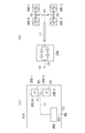
図25に示すメモリモジュールは、同じグループを構成する複数のメモリチップ200と1個のデータレジスタバッファ300がサブモジュール500に集積された構成を有している。このようなサブモジュール500を用いることにより、データ配線L1,L2をサブモジュール基板上に形成することができるため、モジュール基板110の配線密度が緩和される。また、モジュール基板110への部品搭載点数が大幅に少なくなることから、モジュール基板110への実装工程が簡素化される。
The memory module shown in FIG. 25 has a configuration in which a plurality of
図26は、サブモジュール500の構成を示す平面図である。また、図27は、図26に示すY1−Y1'線に沿った断面図である。尚、図26においては、裏面に形成された外部端子を透過的に示している。
FIG. 26 is a plan view showing the configuration of the
図26及び図27に示すサブモジュール500は、サブモジュール基板510と、サブモジュール基板510に搭載された2個のメモリチップ200と、1個のデータレジスタバッファ300と、サブモジュール基板510の裏面に形成された外部端子(ソルダボール)520によって構成されている。メモリチップ200とデータレジスタバッファ300は、封止材530によって封止されている。
A submodule 500 shown in FIGS. 26 and 27 includes a
外部端子520は、データの授受を行うDQボール521と、データレジスタ300に供給すべきコントロール信号の受信を行うControlボール522と、コマンド/アドレス信号の受信を行うCAボール523からなる。DQボール521とControlボール522は、データレジスタバッファ300の搭載領域近傍における裏面に配置されている。一方、CAボール523は、メモリチップ200搭載領域近傍における裏面に配置されている。
The
DQボール521及びControlボール522は、それぞれサブモジュール基板510に形成された内部配線511,512を介してデータレジスタバッファ300に接続される。また、CAボール523は、サブモジュール基板510に形成された内部配線513を介してメモリチップ200に接続される。
The
このようなサブモジュール500を用いれば、メモリチップ200とデータレジスタバッファ300を接続するデータ配線L1,L2をモジュール基板110に形成する必要がなくなる。このため、モジュール基板110の配線自由度が向上する。
If such a
図28は、サブモジュール500の別の構成を示す平面図である。また、図29は、図28に示すY2−Y2'線に沿った断面図である。尚、図28においては、裏面に形成された外部端子を透過的に示している。
FIG. 28 is a plan view showing another configuration of the
図28及び図29に示すサブモジュール500は、図26及び図27に示したサブモジュール500と基本的に同じ構成を有しているが、サブモジュール基板510に8個のメモリチップ200が搭載されている点において相違する。これら8個のメモリチップ200は2個ずつ積層されており、これら4つの積層体がサブモジュール基板510上に平面的に搭載されている。このようなサブモジュール500を用いれば、メモリモジュールの記憶容量を高めることが可能となる。
The
以上、本発明の好ましい実施形態について説明したが、本発明は、上記の実施形態に限定されることなく、本発明の主旨を逸脱しない範囲で種々の変更が可能であり、それらも本発明の範囲内に包含されるものであることはいうまでもない。例えば、上記の実施例では、メモリチップ200として内部にDLL回路を有するものについて説明したが、内部にDLL回路を備えていないメモリチップを用いることができる。この場合、データレジスタバッファ300が有するDLL回路を用いて、入出力のタイミング調整を行なう。
The preferred embodiments of the present invention have been described above, but the present invention is not limited to the above-described embodiments, and various modifications can be made without departing from the spirit of the present invention. Needless to say, it is included in the range. For example, in the above-described embodiment, the
10 情報処理システム
12 メモリコントローラ
12a ライトレベリング回路
12b リードレベリング回路
20 メモリシステム
21 マザーボード
22 メモリスロット
100 メモリモジュール
110 モジュール基板
120 データコネクタ
130 コマンド/アドレス/コントロールコネクタ
200 メモリチップ
300 データレジスタバッファ
301〜304 FIFO回路
320 データレジスタコントロール回路
322 ライトレベリング回路
323 リードレベリング回路
331〜334 セレクタ
340〜342,350〜352 入出力端子
400 コマンド/アドレス/コントロールレジスタバッファ
401,404 入力端子
402,403 出力端子
430 コントロール信号生成回路
500 サブモジュール
L0 データ配線(第1のデータ配線)
L1,L2 データ配線(第2のデータ配線)
L3,L5 コマンド/アドレス/コントロール配線
L4 コントロール配線
DESCRIPTION OF
L1, L2 data wiring (second data wiring)
L3, L5 Command / address / control wiring L4 Control wiring
Claims (11)
前記モジュール基板の長辺に沿って設けられた複数のデータコネクタと、
前記モジュール基板に搭載された複数のメモリチップと、
前記モジュール基板に搭載され、それぞれ2個以上の前記メモリチップが割り当てられた複数のデータレジスタバッファと、
前記モジュール基板に形成され、前記複数のデータコネクタと前記複数のデータレジスタバッファとを接続する複数の第1のデータ配線と、
前記モジュール基板に形成され、前記複数のデータレジスタバッファと前記複数のメモリチップとを接続する複数の第2のデータ配線と、を備え、
各データレジスタバッファと、これに対応する複数の前記データコネクタ及び複数の前記メモリチップは、前記モジュール基板の短辺方向に並べて配置されていることを特徴とするメモリモジュール。 A module board;
A plurality of data connectors provided along the long side of the module substrate;
A plurality of memory chips mounted on the module substrate;
A plurality of data register buffers mounted on the module substrate and each assigned two or more memory chips;
A plurality of first data wirings formed on the module substrate and connecting the plurality of data connectors and the plurality of data register buffers;
A plurality of second data wirings formed on the module substrate and connecting the plurality of data register buffers and the plurality of memory chips;
A memory module, wherein each data register buffer, a plurality of data connectors and a plurality of memory chips corresponding thereto are arranged side by side in the short side direction of the module substrate.
前記モジュール基板に搭載されたコマンド/アドレスレジスタバッファと、をさらに備え、
前記コマンド/アドレスレジスタバッファの入力端子は、前記複数のコマンド/アドレスコネクタに接続され、前記コマンド/アドレスレジスタバッファの第1の出力端子は、前記複数のメモリチップに接続され、前記コマンド/アドレスレジスタバッファの第2の出力端子は、前記複数のデータレジスタバッファに接続されていることを特徴とする請求項1乃至7のいずれか一項に記載のメモリモジュール。 A plurality of command / address connectors provided along the long side of the module substrate;
A command / address register buffer mounted on the module board;
An input terminal of the command / address register buffer is connected to the plurality of command / address connectors, a first output terminal of the command / address register buffer is connected to the plurality of memory chips, and the command / address register The memory module according to claim 1, wherein a second output terminal of the buffer is connected to the plurality of data register buffers.
前記レジスタ回路によってバッファリングされた前記コマンド/アドレス信号が前記第1の出力端子に供給され、
前記コントロール信号生成回路によって生成された前記コントロール信号が前記第2の出力端子に供給されることを特徴とする請求項8に記載のメモリモジュール。 The command / address register buffer generates a control signal based on a register circuit that buffers a command / address signal supplied via the input terminal and a command / address signal supplied via the input terminal. A control signal generation circuit,
The command / address signal buffered by the register circuit is supplied to the first output terminal;
9. The memory module according to claim 8, wherein the control signal generated by the control signal generation circuit is supplied to the second output terminal.
前記コマンド/アドレスレジスタバッファの前記第2の出力端子は、前記複数のデータレジスタバッファに対して共通接続されていることを特徴とする請求項9に記載のメモリモジュール。 The first output terminal of the command / address register buffer is commonly connected to the plurality of memory chips;
10. The memory module according to claim 9, wherein the second output terminal of the command / address register buffer is commonly connected to the plurality of data register buffers.
複数の前記サブモジュール基板が前記モジュール基板に実装されていることを特徴とする請求項1乃至10のいずれか一項に記載のメモリモジュール。 Each data register buffer and a plurality of the memory chips corresponding to each data register buffer are respectively mounted on one submodule substrate,
The memory module according to claim 1, wherein a plurality of the sub module substrates are mounted on the module substrate.
Priority Applications (2)
| Application Number | Priority Date | Filing Date | Title |
|---|---|---|---|
| JP2009136647A JP2010282702A (en) | 2009-06-05 | 2009-06-05 | Memory module |
| US12/801,327 US20100312925A1 (en) | 2009-06-05 | 2010-06-03 | Load reduced memory module |
Applications Claiming Priority (1)
| Application Number | Priority Date | Filing Date | Title |
|---|---|---|---|
| JP2009136647A JP2010282702A (en) | 2009-06-05 | 2009-06-05 | Memory module |
Publications (1)
| Publication Number | Publication Date |
|---|---|
| JP2010282702A true JP2010282702A (en) | 2010-12-16 |
Family
ID=43301550
Family Applications (1)
| Application Number | Title | Priority Date | Filing Date |
|---|---|---|---|
| JP2009136647A Withdrawn JP2010282702A (en) | 2009-06-05 | 2009-06-05 | Memory module |
Country Status (2)
| Country | Link |
|---|---|
| US (1) | US20100312925A1 (en) |
| JP (1) | JP2010282702A (en) |
Cited By (2)
| Publication number | Priority date | Publication date | Assignee | Title |
|---|---|---|---|---|
| JP2014103236A (en) * | 2012-11-20 | 2014-06-05 | Canon Inc | Printed wiring board and printed circuit board |
| US9087555B2 (en) | 2011-08-31 | 2015-07-21 | Ps4 Luxco S.A.R.L. | Semiconductor device and semiconductor chip |
Families Citing this family (6)
| Publication number | Priority date | Publication date | Assignee | Title |
|---|---|---|---|---|
| US9128632B2 (en) | 2009-07-16 | 2015-09-08 | Netlist, Inc. | Memory module with distributed data buffers and method of operation |
| JP2012203807A (en) * | 2011-03-28 | 2012-10-22 | Elpida Memory Inc | Memory module |
| US9412423B2 (en) | 2012-03-15 | 2016-08-09 | Samsung Electronics Co., Ltd. | Memory modules including plural memory devices arranged in rows and module resistor units |
| KR102086465B1 (en) * | 2013-07-11 | 2020-03-09 | 에스케이하이닉스 주식회사 | Semiconductor device and method of driving the same |
| CN110428855B (en) | 2013-07-27 | 2023-09-22 | 奈特力斯股份有限公司 | Memory module with local synchronization |
| EP3058571A1 (en) * | 2013-10-15 | 2016-08-24 | Rambus Inc. | Load reduced memory module |
Family Cites Families (11)
| Publication number | Priority date | Publication date | Assignee | Title |
|---|---|---|---|---|
| US5272664A (en) * | 1993-04-21 | 1993-12-21 | Silicon Graphics, Inc. | High memory capacity DRAM SIMM |
| US6742098B1 (en) * | 2000-10-03 | 2004-05-25 | Intel Corporation | Dual-port buffer-to-memory interface |
| US6721185B2 (en) * | 2001-05-01 | 2004-04-13 | Sun Microsystems, Inc. | Memory module having balanced data I/O contacts pads |
| JP4209130B2 (en) * | 2002-04-09 | 2009-01-14 | 株式会社ザナヴィ・インフォマティクス | Multilayer module board |
| US7102883B2 (en) * | 2003-12-19 | 2006-09-05 | Hewlett-Packard Development Company, L.P. | Memory package |
| US20050213299A1 (en) * | 2004-03-29 | 2005-09-29 | Hardt Thomas T | Memory package |
| US7562271B2 (en) * | 2005-09-26 | 2009-07-14 | Rambus Inc. | Memory system topologies including a buffer device and an integrated circuit memory device |
| JP4389228B2 (en) * | 2006-11-29 | 2009-12-24 | エルピーダメモリ株式会社 | Memory module |
| US7865674B2 (en) * | 2007-08-31 | 2011-01-04 | International Business Machines Corporation | System for enhancing the memory bandwidth available through a memory module |
| US7818497B2 (en) * | 2007-08-31 | 2010-10-19 | International Business Machines Corporation | Buffered memory module supporting two independent memory channels |
| US7821108B2 (en) * | 2008-07-04 | 2010-10-26 | Micron Technology, Inc. | Systems and methods for lowering interconnect capacitance through adjustment of relative signal levels |
-
2009
- 2009-06-05 JP JP2009136647A patent/JP2010282702A/en not_active Withdrawn
-
2010
- 2010-06-03 US US12/801,327 patent/US20100312925A1/en not_active Abandoned
Cited By (3)
| Publication number | Priority date | Publication date | Assignee | Title |
|---|---|---|---|---|
| US9087555B2 (en) | 2011-08-31 | 2015-07-21 | Ps4 Luxco S.A.R.L. | Semiconductor device and semiconductor chip |
| JP2014103236A (en) * | 2012-11-20 | 2014-06-05 | Canon Inc | Printed wiring board and printed circuit board |
| US9907155B2 (en) | 2012-11-20 | 2018-02-27 | Canon Kabushiki Kaisha | Printed wiring board and printed circuit board |
Also Published As
| Publication number | Publication date |
|---|---|
| US20100312925A1 (en) | 2010-12-09 |
Similar Documents
| Publication | Publication Date | Title |
|---|---|---|
| JP2010282511A (en) | Memory module and memory system including the same | |
| JP2010282510A (en) | Memory module | |
| US11621034B2 (en) | Semiconductor memory device having clock generation scheme based on command | |
| US8804442B2 (en) | Semiconductor memory device and read wait time adjustment method thereof, memory system, and semiconductor device | |
| KR102306050B1 (en) | Apparatus and method for adjusting the delay of a command signal path | |
| US7138823B2 (en) | Apparatus and method for independent control of on-die termination for output buffers of a memory device | |
| US8274850B2 (en) | Memory system, semiconductor memory device, and wiring substrate | |
| JP2010282702A (en) | Memory module | |
| US20160162404A1 (en) | Memory module with local synchronization | |
| JP5474458B2 (en) | Semiconductor device and data processing system including the same | |
| KR20200083641A (en) | Apparatus and method comprising memory instructions for semiconductor memory | |
| US11262941B2 (en) | Apparatuses and methods including memory commands for semiconductor memories | |
| JP2007335528A (en) | Laminated semiconductor device | |
| JP2009223854A (en) | Semiconductor device and data processor | |
| KR101961323B1 (en) | On-die termination circuit, semiconductor memory device and memory system including the same | |
| US20110058443A1 (en) | Latency counter, semiconductor memory device including the same, and data processing system | |
| US20180293132A1 (en) | Semiconductor device | |
| US20220358061A1 (en) | Unmatched architecture compensation via digital component delay | |
| US20100299486A1 (en) | Electronic Devices and Methods for Storing Data in a Memory | |
| KR20230149691A (en) | Semiconductor die for controlling on-die-termination of another semiconductor die, and semiconductor devices having the same |
Legal Events
| Date | Code | Title | Description |
|---|---|---|---|
| A300 | Application deemed to be withdrawn because no request for examination was validly filed |
Free format text: JAPANESE INTERMEDIATE CODE: A300 Effective date: 20120807 |