EP1489699A2 - Verbessertes Kontaktelement für fehlergesicherte Verbindung von elektrischen Signalen - Google Patents
Verbessertes Kontaktelement für fehlergesicherte Verbindung von elektrischen Signalen Download PDFInfo
- Publication number
- EP1489699A2 EP1489699A2 EP04104604A EP04104604A EP1489699A2 EP 1489699 A2 EP1489699 A2 EP 1489699A2 EP 04104604 A EP04104604 A EP 04104604A EP 04104604 A EP04104604 A EP 04104604A EP 1489699 A2 EP1489699 A2 EP 1489699A2
- Authority
- EP
- European Patent Office
- Prior art keywords
- contact
- surface portion
- plug
- receptacle
- mating
- Prior art date
- Legal status (The legal status is an assumption and is not a legal conclusion. Google has not performed a legal analysis and makes no representation as to the accuracy of the status listed.)
- Withdrawn
Links
Images


Classifications
-
- H—ELECTRICITY
- H05—ELECTRIC TECHNIQUES NOT OTHERWISE PROVIDED FOR
- H05K—PRINTED CIRCUITS; CASINGS OR CONSTRUCTIONAL DETAILS OF ELECTRIC APPARATUS; MANUFACTURE OF ASSEMBLAGES OF ELECTRICAL COMPONENTS
- H05K1/00—Printed circuits
- H05K1/02—Details
- H05K1/11—Printed elements for providing electric connections to or between printed circuits
- H05K1/117—Pads along the edge of rigid circuit boards, e.g. for pluggable connectors
-
- H—ELECTRICITY
- H01—ELECTRIC ELEMENTS
- H01R—ELECTRICALLY-CONDUCTIVE CONNECTIONS; STRUCTURAL ASSOCIATIONS OF A PLURALITY OF MUTUALLY-INSULATED ELECTRICAL CONNECTING ELEMENTS; COUPLING DEVICES; CURRENT COLLECTORS
- H01R13/00—Details of coupling devices of the kinds covered by groups H01R12/70 or H01R24/00 - H01R33/00
- H01R13/02—Contact members
- H01R13/03—Contact members characterised by the material, e.g. plating, or coating materials
-
- H—ELECTRICITY
- H01—ELECTRIC ELEMENTS
- H01R—ELECTRICALLY-CONDUCTIVE CONNECTIONS; STRUCTURAL ASSOCIATIONS OF A PLURALITY OF MUTUALLY-INSULATED ELECTRICAL CONNECTING ELEMENTS; COUPLING DEVICES; CURRENT COLLECTORS
- H01R13/00—Details of coupling devices of the kinds covered by groups H01R12/70 or H01R24/00 - H01R33/00
- H01R13/66—Structural association with built-in electrical component
- H01R13/665—Structural association with built-in electrical component with built-in electronic circuit
- H01R13/6666—Structural association with built-in electrical component with built-in electronic circuit with built-in overvoltage protection
-
- H—ELECTRICITY
- H01—ELECTRIC ELEMENTS
- H01R—ELECTRICALLY-CONDUCTIVE CONNECTIONS; STRUCTURAL ASSOCIATIONS OF A PLURALITY OF MUTUALLY-INSULATED ELECTRICAL CONNECTING ELEMENTS; COUPLING DEVICES; CURRENT COLLECTORS
- H01R2107/00—Four or more poles
-
- H—ELECTRICITY
- H01—ELECTRIC ELEMENTS
- H01R—ELECTRICALLY-CONDUCTIVE CONNECTIONS; STRUCTURAL ASSOCIATIONS OF A PLURALITY OF MUTUALLY-INSULATED ELECTRICAL CONNECTING ELEMENTS; COUPLING DEVICES; CURRENT COLLECTORS
- H01R2201/00—Connectors or connections adapted for particular applications
- H01R2201/20—Connectors or connections adapted for particular applications for testing or measuring purposes
-
- H—ELECTRICITY
- H01—ELECTRIC ELEMENTS
- H01R—ELECTRICALLY-CONDUCTIVE CONNECTIONS; STRUCTURAL ASSOCIATIONS OF A PLURALITY OF MUTUALLY-INSULATED ELECTRICAL CONNECTING ELEMENTS; COUPLING DEVICES; CURRENT COLLECTORS
- H01R24/00—Two-part coupling devices, or either of their cooperating parts, characterised by their overall structure
- H01R24/60—Contacts spaced along planar side wall transverse to longitudinal axis of engagement
-
- H—ELECTRICITY
- H05—ELECTRIC TECHNIQUES NOT OTHERWISE PROVIDED FOR
- H05K—PRINTED CIRCUITS; CASINGS OR CONSTRUCTIONAL DETAILS OF ELECTRIC APPARATUS; MANUFACTURE OF ASSEMBLAGES OF ELECTRICAL COMPONENTS
- H05K1/00—Printed circuits
- H05K1/16—Printed circuits incorporating printed electric components, e.g. printed resistors, capacitors or inductors
- H05K1/167—Printed circuits incorporating printed electric components, e.g. printed resistors, capacitors or inductors incorporating printed resistors
-
- H—ELECTRICITY
- H05—ELECTRIC TECHNIQUES NOT OTHERWISE PROVIDED FOR
- H05K—PRINTED CIRCUITS; CASINGS OR CONSTRUCTIONAL DETAILS OF ELECTRIC APPARATUS; MANUFACTURE OF ASSEMBLAGES OF ELECTRICAL COMPONENTS
- H05K2201/00—Indexing scheme relating to printed circuits covered by H05K1/00
- H05K2201/03—Conductive materials
- H05K2201/0332—Structure of the conductor
- H05K2201/0335—Layered conductors or foils
- H05K2201/0338—Layered conductor, e.g. layered metal substrate, layered finish layer or layered thin film adhesion layer
-
- Y—GENERAL TAGGING OF NEW TECHNOLOGICAL DEVELOPMENTS; GENERAL TAGGING OF CROSS-SECTIONAL TECHNOLOGIES SPANNING OVER SEVERAL SECTIONS OF THE IPC; TECHNICAL SUBJECTS COVERED BY FORMER USPC CROSS-REFERENCE ART COLLECTIONS [XRACs] AND DIGESTS
- Y10—TECHNICAL SUBJECTS COVERED BY FORMER USPC
- Y10S—TECHNICAL SUBJECTS COVERED BY FORMER USPC CROSS-REFERENCE ART COLLECTIONS [XRACs] AND DIGESTS
- Y10S439/00—Electrical connectors
- Y10S439/931—Conductive coating
-
- Y—GENERAL TAGGING OF NEW TECHNOLOGICAL DEVELOPMENTS; GENERAL TAGGING OF CROSS-SECTIONAL TECHNOLOGIES SPANNING OVER SEVERAL SECTIONS OF THE IPC; TECHNICAL SUBJECTS COVERED BY FORMER USPC CROSS-REFERENCE ART COLLECTIONS [XRACs] AND DIGESTS
- Y10—TECHNICAL SUBJECTS COVERED BY FORMER USPC
- Y10S—TECHNICAL SUBJECTS COVERED BY FORMER USPC CROSS-REFERENCE ART COLLECTIONS [XRACs] AND DIGESTS
- Y10S439/00—Electrical connectors
- Y10S439/951—PCB having detailed leading edge
Definitions
- This device is undesirable for several reasons. First, it requires the use of several contacts of differing lengths, thereby raising manual dexterity problems. Secondly, although the low resistance (i.e. 2-60 ohms) is sufficient to eliminate current surges in power transmissions, it is not sufficient to eliminate the voltage pulse from being introduced into the electronic system. In addition, the thin layer of low resistive material surrounding the thin layer of insulating material introduces an additional problem into the connection between the peripheral device and the electronic system; short capacitance. As explained previously, capacitance is undesirable in a connector.
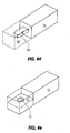
- the resistive portion 12 is generally rectangular shaped and extends across the width W of the plug contact 7.
- the resistive portion 12 comprises a layer of highly resistive material inset into the surface 16 of the plug contact 7, with a first end 11 of the resistive portion 12 exposed to the receptacle 8 and a second end 13 of the resistive portion 12 in contact with the conductive portion 14.
- the first end of the plug 6 is inserted into the cavity of the receptacle 8 .
- the receptacle contact 15 will make first contact with the resistive portion 12. Since it is contemplated that the electronic system will be energized, this will permit energy from the electronic system to begin flowing from the receptacle contact 15 , through the resistive portion 12 and into the conductive portion 14 of the plug contact 7.
- the resistive portion 12 reduces the magnitude of voltage pulses such that they will not present errors into the electronic system, as will be explained in detail hereinafter. A portion of the voltage "seen" by the plug 6 will drop across the resistive portion 12.
- the receptacle contact 15 passes along the surface 16 of the resistive portion 12 until it finally reaches the conductive portion 14 of the plug contact 7 .
- the receptacle contact 15 will be in direct contact with the conductive portion 14 of the plug contact 7 . Accordingly, there will be no voltage drop across the resistive portion 12 of the plug contact 7 .
- the arrangement of the present invention specifically limits the capacitance between the metallic portions of the plug and receptacle contacts 7, 15 , (it bypasses the high resistance), to an acceptably low level. It does this by minimizing their effective coupling area and the effective dielectric constant between them, which is primarily air.
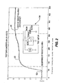
- the resistive portion 12 permits the voltage as seen across the receptacle contact 15 , to increase gradually along the sloped (or curved) portion 93 of the graph as the plug 6 is removed from the receptacle 8. At point 91, the receptacle contact 15 no longer contacts the plug contact 7. Accordingly, 5V is seen by the receptacle contact 15. Curve 93 shows the gradual transition between points 91 and 92 which prevents voltage pulses which will prevent the introduction of errors into the system. Obviously, one skilled in the art would clearly recognize that the graph would be reversed upon insertion of a plug 6 into a receptacle 8 .
- Figure 4b depicts an alternative embodiment with the resistive portion 12 in a stepwise-tapered profile 17. By varying the steps between the steps, the resistive transition curves can be varied as desired.
- Figure 4f depicts a sixth embodiment.
- the conductive body 14 is surrounded by a high resistive housing 30.
- Receptacle contact 15 first makes contact with high resistive housing 30. As the receptacle contact 15 makes contact with conducting portion 14 , the receptacle contact sees essentially no resistance.
Landscapes
- Engineering & Computer Science (AREA)
- Microelectronics & Electronic Packaging (AREA)
- Details Of Connecting Devices For Male And Female Coupling (AREA)
- Coupling Device And Connection With Printed Circuit (AREA)
Applications Claiming Priority (3)
| Application Number | Priority Date | Filing Date | Title |
|---|---|---|---|
| US42400 | 1998-03-13 | ||
| US09/042,400 US6296499B1 (en) | 1998-03-13 | 1998-03-13 | Contact for error resistant coupling of electrical signals |
| EP99301873A EP0949715B1 (de) | 1998-03-13 | 1999-03-11 | Verbessertes Kontaktelement für fehlergesicherte Verbindung von elektrischen Signalen |
Related Parent Applications (1)
| Application Number | Title | Priority Date | Filing Date |
|---|---|---|---|
| EP99301873A Division EP0949715B1 (de) | 1998-03-13 | 1999-03-11 | Verbessertes Kontaktelement für fehlergesicherte Verbindung von elektrischen Signalen |
Publications (2)
| Publication Number | Publication Date |
|---|---|
| EP1489699A2 true EP1489699A2 (de) | 2004-12-22 |
| EP1489699A3 EP1489699A3 (de) | 2004-12-29 |
Family
ID=21921732
Family Applications (2)
| Application Number | Title | Priority Date | Filing Date |
|---|---|---|---|
| EP04104604A Withdrawn EP1489699A3 (de) | 1998-03-13 | 1999-03-11 | Verbessertes Kontaktelement für fehlergesicherte Verbindung von elektrischen Signalen |
| EP99301873A Expired - Lifetime EP0949715B1 (de) | 1998-03-13 | 1999-03-11 | Verbessertes Kontaktelement für fehlergesicherte Verbindung von elektrischen Signalen |
Family Applications After (1)
| Application Number | Title | Priority Date | Filing Date |
|---|---|---|---|
| EP99301873A Expired - Lifetime EP0949715B1 (de) | 1998-03-13 | 1999-03-11 | Verbessertes Kontaktelement für fehlergesicherte Verbindung von elektrischen Signalen |
Country Status (4)
| Country | Link |
|---|---|
| US (2) | US6296499B1 (de) |
| EP (2) | EP1489699A3 (de) |
| JP (1) | JP4345938B2 (de) |
| DE (1) | DE69920561T2 (de) |
Families Citing this family (14)
| Publication number | Priority date | Publication date | Assignee | Title |
|---|---|---|---|---|
| AU3525900A (en) * | 1999-03-12 | 2000-09-28 | Whitaker Corporation, The | A connector assembly providing error resistant coupling of electrical signals |
| JP2001266985A (ja) * | 2000-03-24 | 2001-09-28 | Fujikura Ltd | オス型端子並びにこれを用いたコネクタ及び電気接続構造 |
| US6537092B2 (en) * | 2001-02-02 | 2003-03-25 | Autonetworks Technologies, Ltd | Arc discharge suppressive connector |
| US6857887B1 (en) * | 2003-10-29 | 2005-02-22 | Hewlett-Packard Development Company, L.P. | Current limit engagement apparatus |
| US7651382B2 (en) * | 2006-12-01 | 2010-01-26 | Interconnect Portfolio Llc | Electrical interconnection devices incorporating redundant contact points for reducing capacitive stubs and improved signal integrity |
| US7371091B2 (en) | 2006-06-22 | 2008-05-13 | Honeywell International, Inc. | Method and apparatus for integrated hot swap connector pins for AC and DC electric power systems |
| KR101719699B1 (ko) * | 2010-10-05 | 2017-03-27 | 삼성전자주식회사 | 메모리 모듈 및 이의 제조 방법 |
| WO2012151370A2 (en) * | 2011-05-03 | 2012-11-08 | Cardioinsight Technologies, Inc. | High-voltage resistance of a connector interface |
| WO2012151371A2 (en) * | 2011-05-03 | 2012-11-08 | Cardioinsight Technologies, Inc. | High-voltage resistance for a connector attached to a circuit board |
| CN104871654B (zh) * | 2012-12-18 | 2018-04-06 | 日本电气株式会社 | 电子基板及其接头连接的结构 |
| JP6631169B2 (ja) * | 2015-09-14 | 2020-01-15 | 株式会社オートネットワーク技術研究所 | 通電システム |
| CN108429028B (zh) | 2017-02-13 | 2023-05-30 | 泰连公司 | 抑制电谐振的电连接器 |
| KR102693822B1 (ko) * | 2018-09-03 | 2024-08-12 | 삼성전자 주식회사 | 입출력 단자 및 이를 포함하는 전자장치 |
| US11394146B2 (en) * | 2020-04-07 | 2022-07-19 | Quanta Computer Inc. | Treated connection pins for high speed expansion sockets |
Family Cites Families (13)
| Publication number | Priority date | Publication date | Assignee | Title |
|---|---|---|---|---|
| US1770839A (en) | 1926-11-01 | 1930-07-15 | Gen Electric | Electric contact |
| US2716737A (en) | 1952-06-17 | 1955-08-30 | Garland A Maberry | Electric cable safety connectors |
| US4002496A (en) * | 1974-12-19 | 1977-01-11 | Japan Storage Battery Co., Ltd. | Catalytic device for storage battery |
| US4002396A (en) | 1976-02-13 | 1977-01-11 | Kearney-National, Inc. | Electric connector apparatus |
| US4079440A (en) | 1977-01-19 | 1978-03-14 | Hitachi, Ltd. | Printed circuit board capable of being inserted and withdrawn on on-line status |
| US4117291A (en) | 1977-05-19 | 1978-09-26 | Gte Automatic Electric Laboratories Incorporated | Reed switch |
| US4245270A (en) | 1978-12-26 | 1981-01-13 | Rockwell International Corporation | Circuit card with soft power switch |
| JPS6332881A (ja) | 1986-07-25 | 1988-02-12 | 日本テキサス・インスツルメンツ株式会社 | Icソケツト |
| US4747783A (en) | 1986-10-28 | 1988-05-31 | International Business Machines Corporation | Resistive pin for printed circuit card connector |
| US4897055A (en) * | 1988-11-28 | 1990-01-30 | International Business Machines Corp. | Sequential Connecting device |
| US5236789A (en) * | 1991-07-01 | 1993-08-17 | Olin Corporation | Palladium alloys having utility in electrical applications |
| US5213517A (en) | 1992-02-10 | 1993-05-25 | G & H Technology, Inc. | Separable electrodes with electric arc quenching means |
| US6102742A (en) * | 1998-06-30 | 2000-08-15 | Methode Electronics, Inc. | Electrical connector having variable resistance contacts |
-
1998
- 1998-03-13 US US09/042,400 patent/US6296499B1/en not_active Expired - Lifetime
-
1999
- 1999-03-11 EP EP04104604A patent/EP1489699A3/de not_active Withdrawn
- 1999-03-11 EP EP99301873A patent/EP0949715B1/de not_active Expired - Lifetime
- 1999-03-11 JP JP6505099A patent/JP4345938B2/ja not_active Expired - Fee Related
- 1999-03-11 DE DE69920561T patent/DE69920561T2/de not_active Expired - Lifetime
-
2001
- 2001-08-08 US US09/924,641 patent/US6802729B2/en not_active Expired - Lifetime
Also Published As
| Publication number | Publication date |
|---|---|
| EP0949715A2 (de) | 1999-10-13 |
| EP1489699A3 (de) | 2004-12-29 |
| JPH11297391A (ja) | 1999-10-29 |
| US6802729B2 (en) | 2004-10-12 |
| DE69920561D1 (de) | 2004-11-04 |
| EP0949715B1 (de) | 2004-09-29 |
| DE69920561T2 (de) | 2005-10-27 |
| US20030207627A1 (en) | 2003-11-06 |
| EP0949715A3 (de) | 2000-11-15 |
| US6296499B1 (en) | 2001-10-02 |
| JP4345938B2 (ja) | 2009-10-14 |
Similar Documents
| Publication | Publication Date | Title |
|---|---|---|
| EP0265766B1 (de) | Stecker für einen Verbinder | |
| EP0949715B1 (de) | Verbessertes Kontaktelement für fehlergesicherte Verbindung von elektrischen Signalen | |
| US4992052A (en) | Modular connector system with high contact element density | |
| US6683773B2 (en) | High voltage surge protection element for use with CATV coaxial cable connectors | |
| JP3587193B2 (ja) | 知的に識別可能なコネクタ | |
| US3703604A (en) | Flat conductor transmission cable | |
| EP0733274B1 (de) | Koaxialverbinder mit impedanzsteuerung | |
| WO2006124969A2 (en) | Electrical connector with embedded canted coil spring | |
| US7682192B2 (en) | Electrical receptacle and circuit board with controlled skew | |
| EP0717469A2 (de) | D-sub Verbinder mit Überspannungsschutz | |
| SE433990B (sv) | Overgangskontaktanordning avsedd for hopkoppling av tva olika koaxialkablar | |
| EP0393251B1 (de) | Modulares Verbindersystem mit oberflächenmontierten Verbindern hoher Kontaktelementdichte | |
| US6290543B1 (en) | Telephone adaptor | |
| US6597277B2 (en) | Termination resistor in printed circuit board | |
| WO2000054370A2 (en) | A connector assembly providing error resistant coupling of electrical signals | |
| US6121777A (en) | Apparatus for detecting at least one property of a cable | |
| TWI339457B (en) | Hybrid coupler | |
| JPH07335329A (ja) | 突入電流制限接続器 | |
| EP0858246A3 (de) | Induktionsspule und dieses verwendende kernlose Induktionsofen | |
| US20080057761A1 (en) | A Connector | |
| US4403823A (en) | Electrical contact for position measuring instrument | |
| JPH06243939A (ja) | プリント基板用コネクタの挿抜力・搭載力軽減法 | |
| CN120222097A (zh) | 高速率连接器 | |
| EP0929126A3 (de) | Steckverbinder mit elektronischem Baulelement | |
| JPH11102742A (ja) | コネクタ又はプローブの構造 |
Legal Events
| Date | Code | Title | Description |
|---|---|---|---|
| PUAI | Public reference made under article 153(3) epc to a published international application that has entered the european phase |
Free format text: ORIGINAL CODE: 0009012 |
|
| PUAL | Search report despatched |
Free format text: ORIGINAL CODE: 0009013 |
|
| AC | Divisional application: reference to earlier application |
Ref document number: 0949715 Country of ref document: EP Kind code of ref document: P |
|
| AK | Designated contracting states |
Kind code of ref document: A2 Designated state(s): DE FR GB IE IT |
|
| AK | Designated contracting states |
Kind code of ref document: A3 Designated state(s): DE FR GB IE IT |
|
| 16A | New documents despatched to applicant after publication of the search report |
Effective date: 20041129 |
|
| 17P | Request for examination filed |
Effective date: 20050527 |
|
| AKX | Designation fees paid |
Designated state(s): DE FR GB |
|
| STAA | Information on the status of an ep patent application or granted ep patent |
Free format text: STATUS: THE APPLICATION IS DEEMED TO BE WITHDRAWN |
|
| 18D | Application deemed to be withdrawn |
Effective date: 20060911 |