EP1489699A2 - Improved contact for error resistant coupling of electrical signals - Google Patents
Improved contact for error resistant coupling of electrical signals Download PDFInfo
- Publication number
- EP1489699A2 EP1489699A2 EP04104604A EP04104604A EP1489699A2 EP 1489699 A2 EP1489699 A2 EP 1489699A2 EP 04104604 A EP04104604 A EP 04104604A EP 04104604 A EP04104604 A EP 04104604A EP 1489699 A2 EP1489699 A2 EP 1489699A2
- Authority
- EP
- European Patent Office
- Prior art keywords
- contact
- surface portion
- plug
- receptacle
- mating
- Prior art date
- Legal status (The legal status is an assumption and is not a legal conclusion. Google has not performed a legal analysis and makes no representation as to the accuracy of the status listed.)
- Withdrawn
Links
Images


Classifications
-
- H—ELECTRICITY
- H05—ELECTRIC TECHNIQUES NOT OTHERWISE PROVIDED FOR
- H05K—PRINTED CIRCUITS; CASINGS OR CONSTRUCTIONAL DETAILS OF ELECTRIC APPARATUS; MANUFACTURE OF ASSEMBLAGES OF ELECTRICAL COMPONENTS
- H05K1/00—Printed circuits
- H05K1/02—Details
- H05K1/11—Printed elements for providing electric connections to or between printed circuits
- H05K1/117—Pads along the edge of rigid circuit boards, e.g. for pluggable connectors
-
- H—ELECTRICITY
- H01—ELECTRIC ELEMENTS
- H01R—ELECTRICALLY-CONDUCTIVE CONNECTIONS; STRUCTURAL ASSOCIATIONS OF A PLURALITY OF MUTUALLY-INSULATED ELECTRICAL CONNECTING ELEMENTS; COUPLING DEVICES; CURRENT COLLECTORS
- H01R13/00—Details of coupling devices of the kinds covered by groups H01R12/70 or H01R24/00 - H01R33/00
- H01R13/02—Contact members
- H01R13/03—Contact members characterised by the material, e.g. plating, or coating materials
-
- H—ELECTRICITY
- H01—ELECTRIC ELEMENTS
- H01R—ELECTRICALLY-CONDUCTIVE CONNECTIONS; STRUCTURAL ASSOCIATIONS OF A PLURALITY OF MUTUALLY-INSULATED ELECTRICAL CONNECTING ELEMENTS; COUPLING DEVICES; CURRENT COLLECTORS
- H01R13/00—Details of coupling devices of the kinds covered by groups H01R12/70 or H01R24/00 - H01R33/00
- H01R13/66—Structural association with built-in electrical component
- H01R13/665—Structural association with built-in electrical component with built-in electronic circuit
- H01R13/6666—Structural association with built-in electrical component with built-in electronic circuit with built-in overvoltage protection
-
- H—ELECTRICITY
- H01—ELECTRIC ELEMENTS
- H01R—ELECTRICALLY-CONDUCTIVE CONNECTIONS; STRUCTURAL ASSOCIATIONS OF A PLURALITY OF MUTUALLY-INSULATED ELECTRICAL CONNECTING ELEMENTS; COUPLING DEVICES; CURRENT COLLECTORS
- H01R2107/00—Four or more poles
-
- H—ELECTRICITY
- H01—ELECTRIC ELEMENTS
- H01R—ELECTRICALLY-CONDUCTIVE CONNECTIONS; STRUCTURAL ASSOCIATIONS OF A PLURALITY OF MUTUALLY-INSULATED ELECTRICAL CONNECTING ELEMENTS; COUPLING DEVICES; CURRENT COLLECTORS
- H01R2201/00—Connectors or connections adapted for particular applications
- H01R2201/20—Connectors or connections adapted for particular applications for testing or measuring purposes
-
- H—ELECTRICITY
- H01—ELECTRIC ELEMENTS
- H01R—ELECTRICALLY-CONDUCTIVE CONNECTIONS; STRUCTURAL ASSOCIATIONS OF A PLURALITY OF MUTUALLY-INSULATED ELECTRICAL CONNECTING ELEMENTS; COUPLING DEVICES; CURRENT COLLECTORS
- H01R24/00—Two-part coupling devices, or either of their cooperating parts, characterised by their overall structure
- H01R24/60—Contacts spaced along planar side wall transverse to longitudinal axis of engagement
-
- H—ELECTRICITY
- H05—ELECTRIC TECHNIQUES NOT OTHERWISE PROVIDED FOR
- H05K—PRINTED CIRCUITS; CASINGS OR CONSTRUCTIONAL DETAILS OF ELECTRIC APPARATUS; MANUFACTURE OF ASSEMBLAGES OF ELECTRICAL COMPONENTS
- H05K1/00—Printed circuits
- H05K1/16—Printed circuits incorporating printed electric components, e.g. printed resistor, capacitor, inductor
- H05K1/167—Printed circuits incorporating printed electric components, e.g. printed resistor, capacitor, inductor incorporating printed resistors
-
- H—ELECTRICITY
- H05—ELECTRIC TECHNIQUES NOT OTHERWISE PROVIDED FOR
- H05K—PRINTED CIRCUITS; CASINGS OR CONSTRUCTIONAL DETAILS OF ELECTRIC APPARATUS; MANUFACTURE OF ASSEMBLAGES OF ELECTRICAL COMPONENTS
- H05K2201/00—Indexing scheme relating to printed circuits covered by H05K1/00
- H05K2201/03—Conductive materials
- H05K2201/0332—Structure of the conductor
- H05K2201/0335—Layered conductors or foils
- H05K2201/0338—Layered conductor, e.g. layered metal substrate, layered finish layer, layered thin film adhesion layer
-
- Y—GENERAL TAGGING OF NEW TECHNOLOGICAL DEVELOPMENTS; GENERAL TAGGING OF CROSS-SECTIONAL TECHNOLOGIES SPANNING OVER SEVERAL SECTIONS OF THE IPC; TECHNICAL SUBJECTS COVERED BY FORMER USPC CROSS-REFERENCE ART COLLECTIONS [XRACs] AND DIGESTS
- Y10—TECHNICAL SUBJECTS COVERED BY FORMER USPC
- Y10S—TECHNICAL SUBJECTS COVERED BY FORMER USPC CROSS-REFERENCE ART COLLECTIONS [XRACs] AND DIGESTS
- Y10S439/00—Electrical connectors
- Y10S439/931—Conductive coating
-
- Y—GENERAL TAGGING OF NEW TECHNOLOGICAL DEVELOPMENTS; GENERAL TAGGING OF CROSS-SECTIONAL TECHNOLOGIES SPANNING OVER SEVERAL SECTIONS OF THE IPC; TECHNICAL SUBJECTS COVERED BY FORMER USPC CROSS-REFERENCE ART COLLECTIONS [XRACs] AND DIGESTS
- Y10—TECHNICAL SUBJECTS COVERED BY FORMER USPC
- Y10S—TECHNICAL SUBJECTS COVERED BY FORMER USPC CROSS-REFERENCE ART COLLECTIONS [XRACs] AND DIGESTS
- Y10S439/00—Electrical connectors
- Y10S439/951—PCB having detailed leading edge
Definitions
- This device is undesirable for several reasons. First, it requires the use of several contacts of differing lengths, thereby raising manual dexterity problems. Secondly, although the low resistance (i.e. 2-60 ohms) is sufficient to eliminate current surges in power transmissions, it is not sufficient to eliminate the voltage pulse from being introduced into the electronic system. In addition, the thin layer of low resistive material surrounding the thin layer of insulating material introduces an additional problem into the connection between the peripheral device and the electronic system; short capacitance. As explained previously, capacitance is undesirable in a connector.
- the resistive portion 12 is generally rectangular shaped and extends across the width W of the plug contact 7.
- the resistive portion 12 comprises a layer of highly resistive material inset into the surface 16 of the plug contact 7, with a first end 11 of the resistive portion 12 exposed to the receptacle 8 and a second end 13 of the resistive portion 12 in contact with the conductive portion 14.
- the first end of the plug 6 is inserted into the cavity of the receptacle 8 .
- the receptacle contact 15 will make first contact with the resistive portion 12. Since it is contemplated that the electronic system will be energized, this will permit energy from the electronic system to begin flowing from the receptacle contact 15 , through the resistive portion 12 and into the conductive portion 14 of the plug contact 7.
- the resistive portion 12 reduces the magnitude of voltage pulses such that they will not present errors into the electronic system, as will be explained in detail hereinafter. A portion of the voltage "seen" by the plug 6 will drop across the resistive portion 12.
- the receptacle contact 15 passes along the surface 16 of the resistive portion 12 until it finally reaches the conductive portion 14 of the plug contact 7 .
- the receptacle contact 15 will be in direct contact with the conductive portion 14 of the plug contact 7 . Accordingly, there will be no voltage drop across the resistive portion 12 of the plug contact 7 .
- the arrangement of the present invention specifically limits the capacitance between the metallic portions of the plug and receptacle contacts 7, 15 , (it bypasses the high resistance), to an acceptably low level. It does this by minimizing their effective coupling area and the effective dielectric constant between them, which is primarily air.
- the resistive portion 12 permits the voltage as seen across the receptacle contact 15 , to increase gradually along the sloped (or curved) portion 93 of the graph as the plug 6 is removed from the receptacle 8. At point 91, the receptacle contact 15 no longer contacts the plug contact 7. Accordingly, 5V is seen by the receptacle contact 15. Curve 93 shows the gradual transition between points 91 and 92 which prevents voltage pulses which will prevent the introduction of errors into the system. Obviously, one skilled in the art would clearly recognize that the graph would be reversed upon insertion of a plug 6 into a receptacle 8 .
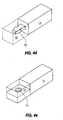
- Figure 4b depicts an alternative embodiment with the resistive portion 12 in a stepwise-tapered profile 17. By varying the steps between the steps, the resistive transition curves can be varied as desired.
- Figure 4f depicts a sixth embodiment.
- the conductive body 14 is surrounded by a high resistive housing 30.
- Receptacle contact 15 first makes contact with high resistive housing 30. As the receptacle contact 15 makes contact with conducting portion 14 , the receptacle contact sees essentially no resistance.
Abstract
Description
- This invention relates generally to electrical connectors for electronic devices. More particularly, the invention relates to electrical contacts for use in electrical connectors to prevent the generation of spurious signals upon mating of the connector.
- Electrical connectors for use with peripheral electronic devices are well known in the art. A recurrent problem with many prior art connectors is the generation of spurious signals upon mating of a peripheral electronic device to an electronic system which is already energized. The connector may induce a voltage pulse into the energized electronic system. The voltage pulse may travel through the electronic system, thereby introducing spurious errors into the system. This problem is known in the art as the "hot plug" problem.
- This condition that causes errors in electronic systems results from the very high data rates and very low energy of the signals within the systems. The input capacitance of the connector, printed circuit board lines and device capacitance of the buffer integrated circuit devices are the basis of the problem. Energy must flow from the system bus to charge this input capacitance, (generally tens of picofarads). When energy is removed from the system bus, a voltage pulse to an adjacent device on the bus occurs, thereby creating errors in the system. The voltage pulse may be no greater than normal signals so no new radiated noise problem is introduced. However, it can cause data to be incorrectly transferred. Accordingly, the interconnections themselves are a large portion of the problem. This problem is universal since it affects both digital and analog electronic devices.
- The prior art has generally addressed the "hot plug" problem by using logic and timing control circuitry, such as that which is disclosed in U.S. Patent No. 4,245,270, to slowly ramp up the voltage within the connecting line. However, providing the additional circuitry is complex and expensive.
- Many connecting schemes require certain portions of the connector to be mated prior to other portions, or in a particular sequence. For example, with respect to power applications, U.S. Patent No. 4,079,440 discloses a circuit board having two connector plugs of differing lengths. The longer connector plug makes initial contact with a power line prior to the shorter plug, which reduces the onset'of power surges. However, this scheme requires manual dexterity and specific insertion and removal timing for proper operation.
- A connector assembly disclosed in U.S. Patent No. 4,747,783 attempts to eliminate timing and control circuitry for power applications. This connector assembly uses a long pin in the "plug" to first make contact with its mating "socket" to gradually increase the voltage to the socket until the entire plug makes mating contact with the socket. The plug comprises a pin having a thin insulating material covering the surface and a thin low resistive material covering the insulating material. When the plug makes initial contact with the socket, the current must pass through the resistive portion of the plug. This permits the electronic components in the peripheral device to charge gradually and eliminates the current surges which may result.
- This device is undesirable for several reasons. First, it requires the use of several contacts of differing lengths, thereby raising manual dexterity problems. Secondly, although the low resistance (i.e. 2-60 ohms) is sufficient to eliminate current surges in power transmissions, it is not sufficient to eliminate the voltage pulse from being introduced into the electronic system. In addition, the thin layer of low resistive material surrounding the thin layer of insulating material introduces an additional problem into the connection between the peripheral device and the electronic system; short capacitance. As explained previously, capacitance is undesirable in a connector.
- It would be desirable to provide a signal connector assembly that would not introduce errors into an electronic system during a hot plug.
- The present invention provides a plug contact having a high resistive portion within a plug for use in a signal connector assembly. When the plug of the assembly first makes contact with the receptacle contacts within a mating receptacle, the high resistive portion of the plug contact prevents a voltage spike. To prevent voltage pulses, resistive portions with resistances ranging from 10KΩ to 1GΩ are necessary depending upon the application. As the plug is further inserted into the receptacle, the energy flow is gradually increased. Eventually, the receptacle contacts within the receptacle pass the high resistive portion and make contact with the conductive portion of the plug contact, thereby permitting transmission of valid signals without the generation of spurious errors. In an alternative embodiment, the receptacle contact, or both the plug contact and the receptacle contact, may have the high resistive portion.
- It is an object of the present invention to provide a connector assembly which permits connection of a peripheral device to an energized electronic system without introducing any spurious errors into that system.
- Other objects and advantages of the present invention will become apparent after reading the detailed description of the presently preferred embodiment.
-
- Figure 1 is an isometric view of a simplified illustration of the present invention.
- Figure 2 is a graph of voltage versus distance traveled along the high resistive portion.
- Figure 3 is a graph of megaohms versus distance traveled along the high resistive portion with curves depicting varying thicknesses of the portion.
- Figure 4a is an alternative embodiment of the present invention with a tapered high resistive portion.
- Figure 4b is an alternative embodiment of the instant invention with a stepwise-tapered high resistive portion.
- Figure 4c is an alternative embodiment of the present invention with a resistive portion of mixed high resistive materials.
- Figure 4d is an alternative embodiment of the present invention with a conductive barb in the high resistive portion.
- Figure 4e is an alternative embodiment of the present invention with the high resistive portion extending into a hole in the conductive portion.
- Figure 4f is an alternative embodiment of the present invention with a high resistive housing.
- Figure 4g is an alternative embodiment of the present invention with a high resistive inset in the housing.
- Figures 4h and 4i are an alternative embodiment of the present invention with a high resistance inset in the housing.
- Figure 5 is an illustration of the instant invention utilized on a circuit board.
- Figure 6 is an illustration of the instant invention being used on a cylindrical connector.
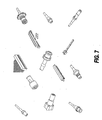
- Figure 7 is an illustration of the various prior art connectors.
-
- The preferred embodiment will be described with reference to the drawing figures wherein like numerals represent like elements throughout.
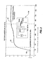
- Referring to Figure 1, the preferred embodiment of the connector assembly of the present invention comprises a
plug 6 for mating with acorresponding receptacle 8. It should be recognized that although only oneplug contact 7 is shown in detail for simplicity, there are typically at least two ormore plug contacts 7 within everyplug 6 for mating withcorresponding receptacle contacts 15. The shape of theplug 6 is not central to the present invention. For simplicity, theplug 6 andplug contact 7 are illustrated as rectangular, although those of skill in the art will realize that many other shapes could be used without departing from the spirit of the present invention. Theplug contact 7 comprises aconductive portion 14 which can be made from any conductive material, (such as brass, nickel, gold, copper or a superconductor, etc.) and a highlyresistive portion 12. Theresistive portion 12 is generally rectangular shaped and extends across the width W of theplug contact 7. Theresistive portion 12 comprises a layer of highly resistive material inset into thesurface 16 of theplug contact 7, with afirst end 11 of theresistive portion 12 exposed to thereceptacle 8 and asecond end 13 of theresistive portion 12 in contact with theconductive portion 14. - A
typical receptacle 8 includes areceptacle contact 15 for eachcorresponding plug contact 7 which electrically mates with itscorresponding receptacle contact 15 as theplug 6 of the peripheral device (not shown) is inserted intoreceptacle 8 of the electronic system (not shown). - In operation, the first end of the
plug 6 is inserted into the cavity of thereceptacle 8. Thereceptacle contact 15 will make first contact with theresistive portion 12. Since it is contemplated that the electronic system will be energized, this will permit energy from the electronic system to begin flowing from thereceptacle contact 15, through theresistive portion 12 and into theconductive portion 14 of theplug contact 7. Theresistive portion 12 reduces the magnitude of voltage pulses such that they will not present errors into the electronic system, as will be explained in detail hereinafter. A portion of the voltage "seen" by theplug 6 will drop across theresistive portion 12. As theplug 6 is inserted further into thereceptacle 8, thereceptacle contact 15 passes along thesurface 16 of theresistive portion 12 until it finally reaches theconductive portion 14 of theplug contact 7. When theplug 6 is fully inserted into thereceptacle 8, thereceptacle contact 15 will be in direct contact with theconductive portion 14 of theplug contact 7. Accordingly, there will be no voltage drop across theresistive portion 12 of theplug contact 7. With respect to capacitance, the arrangement of the present invention specifically limits the capacitance between the metallic portions of the plug andreceptacle contacts - A primary aspect of preventing a voltage pulse is to reduce the initial voltage seen by
plug contact 7 upon insertion of theplug 6 into thereceptacle 8. Referring to thetest setup 94 and the graph of Figure 2, it can clearly be seen that theresistive portion 12 reduces the initial voltage seen by thereceptacle contact 15. The graph represents the voltage seen by thereceptacle contact 15 as theplug 6 is removed from thereceptacle 8. Referring to the portion of the graph to the left ofpoint 92, this shows a short circuit voltage of 0V across theplug contact 7 while theplug contact 7 is in full contact with thereceptacle contact 15. Atpoint 92, thereceptacle contact 15 contacts theresistive portion 12. Theresistive portion 12 permits the voltage as seen across thereceptacle contact 15, to increase gradually along the sloped (or curved)portion 93 of the graph as theplug 6 is removed from thereceptacle 8. Atpoint 91, thereceptacle contact 15 no longer contacts theplug contact 7. Accordingly, 5V is seen by thereceptacle contact 15.Curve 93 shows the gradual transition betweenpoints plug 6 into areceptacle 8. - The high resistance of
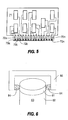
resistive portion 12 limits the rate of flow of current from the system bus to the "cold" device being hot-plugged into the system. The evidence of too fast a current transfer is a transient voltage pulse at the connection to the operating system. The transient voltage pulse decays as it propagates along the system bus, primarily because the bus and other attached devices are sources of charge. Accordingly, the high resistance slows the charge transfer enough to provide time for the charge to be adequately replaced. If the voltage cannot dip below the sensing threshold of an adjacent device, an error cannot occur. - Figure 3 is a graph of the electrical resistance as measured from the end of the
plug contact 7. This graph is based on aresistive portion 12 of a rectangular shape 0.33mm (13 mils) wide and 0.38 mm (15 mils) long. As shown, the resistance increases as the thickness of theresistive portion 12 increases. Referring tocurve 20, when a resistive portion thickness of 0.20 mm (8 mils) is used, a resistance of 10M Ω is achieved at thefirst end 11 of theplug contact 7, which gradually decreases until thesecond end 13 is reached where the resistance is nominally zero. - By changing both the resistivity and the thickness of the
resistive portion 12, as those skilled in the art will realize, the present invention can be adapted to different uses and applications. However, it is also extremely important to reduce the short capacitance to a negligible level. The short capacitance is reduced by keeping the thickness of theinlay 12 relatively thick, [i.e. in applying the present invention to a SCSI Bus, typically approximately 0.13 mm (5 mils)]. By adjusting the resistivity and thickness of the resistive portion, connector assemblies can be created with desirable characteristics by preventing voltage surges for various types of signals and applications. - Alternative embodiments of the present invention are shown in Figures 4a-4i. In the embodiment depicted in Figure 4a, the
resistive portion 12 has a tapered profile. By varying the shape of the tapered profile of the resistive portion, the resistive transition curves that result as thereceptacle contact 15 passes over theresistive portion 12 can be varied as desired for a particular application. - Figure 4b depicts an alternative embodiment with the
resistive portion 12 in a stepwise-taperedprofile 17. By varying the steps between the steps, the resistive transition curves can be varied as desired. - A third alternative embodiment is shown in Figure 4c. The
resistive portion 12 consists of two or more materials with varying resistivities. - Figure 4d, a fourth alternative embodiment shows, the
resistive portion 12 extending from the conductingportion 14. A conductingbarb 18 extends from the conductingbody 14 into theresistive portion 12. A fifth alternative embodiment, Figure 4e, has theresistive portion 12 extending into ahole 19 in the conductingportion 14. As those skilled in the art will note many other variations are possible without departing from the spirit of the invention. These varying embodiments can be used for varying the resistive transition curves for differing applications. - Figure 4f depicts a sixth embodiment. The
conductive body 14 is surrounded by a highresistive housing 30.Receptacle contact 15 first makes contact with highresistive housing 30. As thereceptacle contact 15 makes contact with conductingportion 14, the receptacle contact sees essentially no resistance. - In Figure 4g, the
housing 30 is non-conductive. However, highresistive portions 12 make initial contact withreceptacle contact 15. The high resistive portions' 12 are electrically connected and may be physically connected (not shown) to conductingportion 14. - Figures 4h and 4i depict a
plug 7 having ahousing 85 surrounding a firsthigh resistance 31 portion and a secondlow resistance portion 32. Upon full mating, thereceptacle contact 15 is in full contact with thelow resistance portion 32. - Figure 5 illustrates that the present instant invention may also be used with the contacts on a printed circuit board. The
resistive portions 70a-n of the instant invention may be employed in one ormore plug contacts 72a-n on a conventional printed circuit board 71. Figure 6 shows that the present invention may be adapted to various shaped applications. For instance, aplug 83 with a cylindrical shape with aresistive portion 81 andconductive portion 82.Receptacle contacts 84 within thereceptacle 85 make contact with theresistive portion 81 prior to theconductive portion 82. - Figure 7 illustrates some prior art electrical connectors. The size and shape of the connectors vary. As those skilled in the art will realize, the present invention can be used with the contacts within these various connectors.
- Although the invention has been described in part by making detailed reference to certain specific embodiments, such details are intended to be instructive rather than restrictive. It will be appreciated by those skilled in the art that many variations may be made in the structure and mode of operation without departing from the scope of the invention as disclosed in the teachings herein.
Claims (12)
- An electrical contact (7) comprising:a conductive portion (14) of a material having a first resistivity; anda resistive portion (12) of a material having a second resistivity that is significantly greater than the first resistivity, the resistive portion (12) being exposed for direct engagement with a mating contact (15) and being in direct contact with the conductive portion (14) to allow current flow along a shortest path between the mating contact (15) and the conductive portion (14).
- A connector assembly comprising:a first contact (7) and a second contact (15) configured to mate with the first contact (7);the first contact (7) configured for slidingly engaging the second contact (15) to continuously define an electric connection between the first contact (7) and the second contact (15) and comprising conductive material (14) and a resistive material (12) exposed for direct, initial engagement with the second contact (15) to produce an initial high resistance connection along a shortest path between the second contact (15) and the conductive material (14).
- A contact (7) for error resistant coupling of electrical signals comprising:said leading surface portion (12) being defined by a material having a resistance of at least 10K Q; anda contact mating portion having selectively configured surface portions for slidingly engaging a mating contact (15) to continuously define an electric signal connection between the contact (7) and the mating contact (15)comprising:a leading surface portion (12) for initial engagement with the mating contact (15) to produce an initial high resistance connection, anda trailing surface portion (14) for engagement with the mating contact (15) when in a fully mated relationship to produce a relatively low resistance connection;
said trailing surface portion (14) being defined by a conductive material. - A contact according to claim 3 wherein said leading surface portion (12) is contiguous with said trailing surface portion (14) to define a continuos surface (16).
- A contact according to claim 3 or 4 further comprising an intermediate surface portion defined by a material of lower resistivity than said leading surface material (14);
wherein said mating contact (15) sequentially engages said leading surface portion (12), said intermediate surface portion and said trailing surface portion (14). - A contact according to claim 5 wherein said intermediate surface portion is contiguous with said leading surface portion (12) and said trailing surface portion (14) to define a continuous surface (16).
- A contact according to any one of claims 3 to 6 wherein said leading surface portion (12) has decreasing thickness along the direction of sliding engagement.
- A contact according to any one of claims 3 to 7 wherein said leading surface portion (12) has decreasing resistivity along the direction of sliding engagement.
- A contact according to any one of claims 3 to 8 wherein the leading surface portion,material (12) is inset in the trailing surface portion material (14)
- A contact according to any one of claims 3 to 9 wherein said trailing surface portion material (14) has a protrusion (18) extending into said leading surface portion material (12).
- A contact according to any one of claims 3 to 9 wherein said leading surface portion material (12) has a protrusion extending into said trailing surface portion material (14).
- A contact according to claim 3 wherein said leading surface portion is defined by a material having a resistance between 10KΩand 1GΩ.
Applications Claiming Priority (3)
| Application Number | Priority Date | Filing Date | Title |
|---|---|---|---|
| US42400 | 1998-03-13 | ||
| US09/042,400 US6296499B1 (en) | 1998-03-13 | 1998-03-13 | Contact for error resistant coupling of electrical signals |
| EP99301873A EP0949715B1 (en) | 1998-03-13 | 1999-03-11 | Improved contact for error resistant coupling of electrical signals |
Related Parent Applications (1)
| Application Number | Title | Priority Date | Filing Date |
|---|---|---|---|
| EP99301873A Division EP0949715B1 (en) | 1998-03-13 | 1999-03-11 | Improved contact for error resistant coupling of electrical signals |
Publications (2)
| Publication Number | Publication Date |
|---|---|
| EP1489699A2 true EP1489699A2 (en) | 2004-12-22 |
| EP1489699A3 EP1489699A3 (en) | 2004-12-29 |
Family
ID=21921732
Family Applications (2)
| Application Number | Title | Priority Date | Filing Date |
|---|---|---|---|
| EP99301873A Expired - Lifetime EP0949715B1 (en) | 1998-03-13 | 1999-03-11 | Improved contact for error resistant coupling of electrical signals |
| EP04104604A Withdrawn EP1489699A3 (en) | 1998-03-13 | 1999-03-11 | Improved contact for error resistant coupling of electrical signals |
Family Applications Before (1)
| Application Number | Title | Priority Date | Filing Date |
|---|---|---|---|
| EP99301873A Expired - Lifetime EP0949715B1 (en) | 1998-03-13 | 1999-03-11 | Improved contact for error resistant coupling of electrical signals |
Country Status (4)
| Country | Link |
|---|---|
| US (2) | US6296499B1 (en) |
| EP (2) | EP0949715B1 (en) |
| JP (1) | JP4345938B2 (en) |
| DE (1) | DE69920561T2 (en) |
Families Citing this family (14)
| Publication number | Priority date | Publication date | Assignee | Title |
|---|---|---|---|---|
| WO2000054370A2 (en) * | 1999-03-12 | 2000-09-14 | The Whitaker Corporation | A connector assembly providing error resistant coupling of electrical signals |
| JP2001266985A (en) * | 2000-03-24 | 2001-09-28 | Fujikura Ltd | Male terminal and connector and electric connection structure using it |
| US6537092B2 (en) * | 2001-02-02 | 2003-03-25 | Autonetworks Technologies, Ltd | Arc discharge suppressive connector |
| US6857887B1 (en) * | 2003-10-29 | 2005-02-22 | Hewlett-Packard Development Company, L.P. | Current limit engagement apparatus |
| US7651382B2 (en) * | 2006-12-01 | 2010-01-26 | Interconnect Portfolio Llc | Electrical interconnection devices incorporating redundant contact points for reducing capacitive stubs and improved signal integrity |
| US7371091B2 (en) | 2006-06-22 | 2008-05-13 | Honeywell International, Inc. | Method and apparatus for integrated hot swap connector pins for AC and DC electric power systems |
| KR101719699B1 (en) * | 2010-10-05 | 2017-03-27 | 삼성전자주식회사 | Memory module and method of manufacturing the memory module |
| US9472879B2 (en) | 2011-05-03 | 2016-10-18 | Cardioinsight Technologies, Inc. | High-voltage resistance of a connector interface |
| WO2012151371A2 (en) * | 2011-05-03 | 2012-11-08 | Cardioinsight Technologies, Inc. | High-voltage resistance for a connector attached to a circuit board |
| WO2014097580A1 (en) * | 2012-12-18 | 2014-06-26 | 日本電気株式会社 | Electronic circuit board and connector connection structure |
| JP6631169B2 (en) * | 2015-09-14 | 2020-01-15 | 株式会社オートネットワーク技術研究所 | Power supply system |
| CN108429028B (en) | 2017-02-13 | 2023-05-30 | 泰连公司 | Electrical connector for suppressing electrical resonance |
| KR20200026583A (en) * | 2018-09-03 | 2020-03-11 | 삼성전자주식회사 | In and out port and electronic device including the same |
| US11394146B2 (en) * | 2020-04-07 | 2022-07-19 | Quanta Computer Inc. | Treated connection pins for high speed expansion sockets |
Citations (3)
| Publication number | Priority date | Publication date | Assignee | Title |
|---|---|---|---|---|
| US2716737A (en) * | 1952-06-17 | 1955-08-30 | Garland A Maberry | Electric cable safety connectors |
| US4002496A (en) * | 1974-12-19 | 1977-01-11 | Japan Storage Battery Co., Ltd. | Catalytic device for storage battery |
| EP0371206A2 (en) * | 1988-11-28 | 1990-06-06 | International Business Machines Corporation | Sequential connecting device |
Family Cites Families (10)
| Publication number | Priority date | Publication date | Assignee | Title |
|---|---|---|---|---|
| US1770839A (en) | 1926-11-01 | 1930-07-15 | Gen Electric | Electric contact |
| US4002396A (en) | 1976-02-13 | 1977-01-11 | Kearney-National, Inc. | Electric connector apparatus |
| US4079440A (en) | 1977-01-19 | 1978-03-14 | Hitachi, Ltd. | Printed circuit board capable of being inserted and withdrawn on on-line status |
| US4117291A (en) | 1977-05-19 | 1978-09-26 | Gte Automatic Electric Laboratories Incorporated | Reed switch |
| US4245270A (en) | 1978-12-26 | 1981-01-13 | Rockwell International Corporation | Circuit card with soft power switch |
| JPS6332881A (en) | 1986-07-25 | 1988-02-12 | 日本テキサス・インスツルメンツ株式会社 | Ic socket |
| US4747783A (en) | 1986-10-28 | 1988-05-31 | International Business Machines Corporation | Resistive pin for printed circuit card connector |
| US5236789A (en) * | 1991-07-01 | 1993-08-17 | Olin Corporation | Palladium alloys having utility in electrical applications |
| US5213517A (en) | 1992-02-10 | 1993-05-25 | G & H Technology, Inc. | Separable electrodes with electric arc quenching means |
| US6102742A (en) * | 1998-06-30 | 2000-08-15 | Methode Electronics, Inc. | Electrical connector having variable resistance contacts |
-
1998
- 1998-03-13 US US09/042,400 patent/US6296499B1/en not_active Expired - Lifetime
-
1999
- 1999-03-11 JP JP6505099A patent/JP4345938B2/en not_active Expired - Fee Related
- 1999-03-11 DE DE69920561T patent/DE69920561T2/en not_active Expired - Lifetime
- 1999-03-11 EP EP99301873A patent/EP0949715B1/en not_active Expired - Lifetime
- 1999-03-11 EP EP04104604A patent/EP1489699A3/en not_active Withdrawn
-
2001
- 2001-08-08 US US09/924,641 patent/US6802729B2/en not_active Expired - Lifetime
Patent Citations (3)
| Publication number | Priority date | Publication date | Assignee | Title |
|---|---|---|---|---|
| US2716737A (en) * | 1952-06-17 | 1955-08-30 | Garland A Maberry | Electric cable safety connectors |
| US4002496A (en) * | 1974-12-19 | 1977-01-11 | Japan Storage Battery Co., Ltd. | Catalytic device for storage battery |
| EP0371206A2 (en) * | 1988-11-28 | 1990-06-06 | International Business Machines Corporation | Sequential connecting device |
Non-Patent Citations (1)
| Title |
|---|
| "POLYMER HOT PLUG DEVICE" IBM TECHNICAL DISCLOSURE BULLETIN, IBM CORP. NEW YORK, US, vol. 32, no. 2, 1 July 1989 (1989-07-01), pages 307-308, XP000033437 ISSN: 0018-8689 * |
Also Published As
| Publication number | Publication date |
|---|---|
| EP1489699A3 (en) | 2004-12-29 |
| US6296499B1 (en) | 2001-10-02 |
| DE69920561D1 (en) | 2004-11-04 |
| EP0949715B1 (en) | 2004-09-29 |
| JP4345938B2 (en) | 2009-10-14 |
| EP0949715A2 (en) | 1999-10-13 |
| US6802729B2 (en) | 2004-10-12 |
| DE69920561T2 (en) | 2005-10-27 |
| JPH11297391A (en) | 1999-10-29 |
| EP0949715A3 (en) | 2000-11-15 |
| US20030207627A1 (en) | 2003-11-06 |
Similar Documents
| Publication | Publication Date | Title |
|---|---|---|
| EP0265766B1 (en) | A connector plug | |
| EP0949715B1 (en) | Improved contact for error resistant coupling of electrical signals | |
| US4992052A (en) | Modular connector system with high contact element density | |
| US7102868B2 (en) | High voltage surge protection element for use with CATV coaxial cable connectors | |
| JP3587193B2 (en) | Intelligently identifiable connector | |
| US3703604A (en) | Flat conductor transmission cable | |
| EP0733274B1 (en) | Coaxial connector with impedance control | |
| US5766036A (en) | Impedance matched cable assembly having latching subassembly | |
| EP0284820A3 (en) | Electrically connecting member, and electric circuit member and electric circuit device with the connecting member | |
| US5237293A (en) | Self-terminating coaxial cable connector | |
| EP0698305A1 (en) | High-density connector | |
| US7682192B2 (en) | Electrical receptacle and circuit board with controlled skew | |
| EP0790673A3 (en) | Electrical connector with sensing terminal system | |
| JP4368015B2 (en) | Rod glow plug | |
| SE433990B (en) | TRANSITIONAL CONNECTOR DEVICE FOR CONNECTING TWO DIFFERENT COAXIAL CABLES | |
| EP0393251B1 (en) | Modular connector system with high contact element density surface mounted connectors | |
| US6597277B2 (en) | Termination resistor in printed circuit board | |
| WO1998027625A1 (en) | Telephone adaptor | |
| TWI339457B (en) | Hybrid coupler | |
| US6262372B1 (en) | Electrical terminal with integral PTC element | |
| CN1950978B (en) | A connector | |
| WO2000054370A2 (en) | A connector assembly providing error resistant coupling of electrical signals | |
| EP0874528A3 (en) | Connection pin | |
| JPH0862276A (en) | Module of electric apparatus to detect property of cable | |
| EP1201902A3 (en) | Electrical connection for fuel injectors |
Legal Events
| Date | Code | Title | Description |
|---|---|---|---|
| PUAI | Public reference made under article 153(3) epc to a published international application that has entered the european phase |
Free format text: ORIGINAL CODE: 0009012 |
|
| PUAL | Search report despatched |
Free format text: ORIGINAL CODE: 0009013 |
|
| AC | Divisional application: reference to earlier application |
Ref document number: 0949715 Country of ref document: EP Kind code of ref document: P |
|
| AK | Designated contracting states |
Kind code of ref document: A2 Designated state(s): DE FR GB IE IT |
|
| AK | Designated contracting states |
Kind code of ref document: A3 Designated state(s): DE FR GB IE IT |
|
| 16A | New documents despatched to applicant after publication of the search report |
Effective date: 20041129 |
|
| 17P | Request for examination filed |
Effective date: 20050527 |
|
| AKX | Designation fees paid |
Designated state(s): DE FR GB |
|
| STAA | Information on the status of an ep patent application or granted ep patent |
Free format text: STATUS: THE APPLICATION IS DEEMED TO BE WITHDRAWN |
|
| 18D | Application deemed to be withdrawn |
Effective date: 20060911 |