EP1488260B1 - Interlocking profiled fastening foils used as waveguides for illumination purposes - Google Patents
Interlocking profiled fastening foils used as waveguides for illumination purposes Download PDFInfo
- Publication number
- EP1488260B1 EP1488260B1 EP03704001A EP03704001A EP1488260B1 EP 1488260 B1 EP1488260 B1 EP 1488260B1 EP 03704001 A EP03704001 A EP 03704001A EP 03704001 A EP03704001 A EP 03704001A EP 1488260 B1 EP1488260 B1 EP 1488260B1
- Authority
- EP
- European Patent Office
- Prior art keywords
- light
- light guide
- layers
- layer
- elements
- Prior art date
- Legal status (The legal status is an assumption and is not a legal conclusion. Google has not performed a legal analysis and makes no representation as to the accuracy of the status listed.)
- Expired - Lifetime
Links
- 238000005286 illumination Methods 0.000 title description 5
- 239000011888 foil Substances 0.000 title 1
- 239000000463 material Substances 0.000 claims description 29
- 239000000654 additive Substances 0.000 claims description 9
- 230000000996 additive effect Effects 0.000 claims description 8
- -1 polypropylene Polymers 0.000 claims description 8
- 238000000576 coating method Methods 0.000 claims description 7
- 230000003287 optical effect Effects 0.000 claims description 6
- 239000004743 Polypropylene Substances 0.000 claims description 4
- 239000003086 colorant Substances 0.000 claims description 4
- 229920001155 polypropylene Polymers 0.000 claims description 4
- 239000012528 membrane Substances 0.000 description 29
- 238000003491 array Methods 0.000 description 20
- 230000000694 effects Effects 0.000 description 18
- 238000001125 extrusion Methods 0.000 description 11
- 238000000034 method Methods 0.000 description 8
- 230000008901 benefit Effects 0.000 description 7
- 230000000994 depressogenic effect Effects 0.000 description 7
- 230000008569 process Effects 0.000 description 5
- 230000004888 barrier function Effects 0.000 description 4
- 238000000465 moulding Methods 0.000 description 4
- 239000000758 substrate Substances 0.000 description 4
- 239000011248 coating agent Substances 0.000 description 3
- 235000009508 confectionery Nutrition 0.000 description 3
- 238000010586 diagram Methods 0.000 description 3
- 230000033001 locomotion Effects 0.000 description 3
- 238000003825 pressing Methods 0.000 description 3
- 230000004044 response Effects 0.000 description 3
- 230000000007 visual effect Effects 0.000 description 3
- 230000005540 biological transmission Effects 0.000 description 2
- 230000001413 cellular effect Effects 0.000 description 2
- 238000004049 embossing Methods 0.000 description 2
- 238000001746 injection moulding Methods 0.000 description 2
- 229920000728 polyester Polymers 0.000 description 2
- 238000010791 quenching Methods 0.000 description 2
- 239000003351 stiffener Substances 0.000 description 2
- 230000002123 temporal effect Effects 0.000 description 2
- IAYPIBMASNFSPL-UHFFFAOYSA-N Ethylene oxide Chemical compound C1CO1 IAYPIBMASNFSPL-UHFFFAOYSA-N 0.000 description 1
- 239000004677 Nylon Substances 0.000 description 1
- 229920003171 Poly (ethylene oxide) Polymers 0.000 description 1
- 239000004952 Polyamide Substances 0.000 description 1
- 239000004695 Polyether sulfone Substances 0.000 description 1
- 229920000491 Polyphenylsulfone Polymers 0.000 description 1
- 239000004793 Polystyrene Substances 0.000 description 1
- NIXOWILDQLNWCW-UHFFFAOYSA-N acrylic acid group Chemical group C(C=C)(=O)O NIXOWILDQLNWCW-UHFFFAOYSA-N 0.000 description 1
- XECAHXYUAAWDEL-UHFFFAOYSA-N acrylonitrile butadiene styrene Chemical compound C=CC=C.C=CC#N.C=CC1=CC=CC=C1 XECAHXYUAAWDEL-UHFFFAOYSA-N 0.000 description 1
- 239000004676 acrylonitrile butadiene styrene Substances 0.000 description 1
- 229920000122 acrylonitrile butadiene styrene Polymers 0.000 description 1
- 239000000853 adhesive Substances 0.000 description 1
- 230000001070 adhesive effect Effects 0.000 description 1
- 230000008859 change Effects 0.000 description 1
- 239000003795 chemical substances by application Substances 0.000 description 1
- 238000000748 compression moulding Methods 0.000 description 1
- 230000000881 depressing effect Effects 0.000 description 1
- XSMJZKTTXZAXHD-UHFFFAOYSA-N ethene;2-methylprop-2-enoic acid Chemical compound C=C.CC(=C)C(O)=O XSMJZKTTXZAXHD-UHFFFAOYSA-N 0.000 description 1
- 125000001301 ethoxy group Chemical group [H]C([H])([H])C([H])([H])O* 0.000 description 1
- 239000000835 fiber Substances 0.000 description 1
- 229920002313 fluoropolymer Polymers 0.000 description 1
- 239000011521 glass Substances 0.000 description 1
- 230000002209 hydrophobic effect Effects 0.000 description 1
- 238000003754 machining Methods 0.000 description 1
- 238000004519 manufacturing process Methods 0.000 description 1
- 239000011159 matrix material Substances 0.000 description 1
- 239000002184 metal Substances 0.000 description 1
- 229920001778 nylon Polymers 0.000 description 1
- 239000004033 plastic Substances 0.000 description 1
- 229920003023 plastic Polymers 0.000 description 1
- 229920002492 poly(sulfone) Polymers 0.000 description 1
- 229920002647 polyamide Polymers 0.000 description 1
- 229920001748 polybutylene Polymers 0.000 description 1
- 239000004417 polycarbonate Substances 0.000 description 1
- 229920000515 polycarbonate Polymers 0.000 description 1
- 229920006393 polyether sulfone Polymers 0.000 description 1
- 229920000642 polymer Polymers 0.000 description 1
- 229920000306 polymethylpentene Polymers 0.000 description 1
- 239000011116 polymethylpentene Substances 0.000 description 1
- 229920000098 polyolefin Polymers 0.000 description 1
- 229920001296 polysiloxane Polymers 0.000 description 1
- 229920002223 polystyrene Polymers 0.000 description 1
- 229920002635 polyurethane Polymers 0.000 description 1
- 239000004814 polyurethane Substances 0.000 description 1
- 239000004800 polyvinyl chloride Substances 0.000 description 1
- 229920000915 polyvinyl chloride Polymers 0.000 description 1
- SCUZVMOVTVSBLE-UHFFFAOYSA-N prop-2-enenitrile;styrene Chemical compound C=CC#N.C=CC1=CC=CC=C1 SCUZVMOVTVSBLE-UHFFFAOYSA-N 0.000 description 1
- 239000004065 semiconductor Substances 0.000 description 1
- 238000005728 strengthening Methods 0.000 description 1
- 229920000638 styrene acrylonitrile Polymers 0.000 description 1
- 229920006132 styrene block copolymer Polymers 0.000 description 1
- 239000000126 substance Substances 0.000 description 1
- 239000004094 surface-active agent Substances 0.000 description 1
- 238000003856 thermoforming Methods 0.000 description 1
- 238000012876 topography Methods 0.000 description 1
- 239000012780 transparent material Substances 0.000 description 1
- XLYOFNOQVPJJNP-UHFFFAOYSA-N water Substances O XLYOFNOQVPJJNP-UHFFFAOYSA-N 0.000 description 1
Images


Classifications
-
- G—PHYSICS
- G02—OPTICS
- G02B—OPTICAL ELEMENTS, SYSTEMS OR APPARATUS
- G02B6/00—Light guides; Structural details of arrangements comprising light guides and other optical elements, e.g. couplings
- G02B6/0001—Light guides; Structural details of arrangements comprising light guides and other optical elements, e.g. couplings specially adapted for lighting devices or systems
- G02B6/0011—Light guides; Structural details of arrangements comprising light guides and other optical elements, e.g. couplings specially adapted for lighting devices or systems the light guides being planar or of plate-like form
- G02B6/0081—Mechanical or electrical aspects of the light guide and light source in the lighting device peculiar to the adaptation to planar light guides, e.g. concerning packaging
- G02B6/0095—Light guides as housings, housing portions, shelves, doors, tiles, windows, or the like
-
- H—ELECTRICITY
- H01—ELECTRIC ELEMENTS
- H01H—ELECTRIC SWITCHES; RELAYS; SELECTORS; EMERGENCY PROTECTIVE DEVICES
- H01H13/00—Switches having rectilinearly-movable operating part or parts adapted for pushing or pulling in one direction only, e.g. push-button switch
- H01H13/70—Switches having rectilinearly-movable operating part or parts adapted for pushing or pulling in one direction only, e.g. push-button switch having a plurality of operating members associated with different sets of contacts, e.g. keyboard
- H01H13/702—Switches having rectilinearly-movable operating part or parts adapted for pushing or pulling in one direction only, e.g. push-button switch having a plurality of operating members associated with different sets of contacts, e.g. keyboard with contacts carried by or formed from layers in a multilayer structure, e.g. membrane switches
-
- H—ELECTRICITY
- H01—ELECTRIC ELEMENTS
- H01H—ELECTRIC SWITCHES; RELAYS; SELECTORS; EMERGENCY PROTECTIVE DEVICES
- H01H9/00—Details of switching devices, not covered by groups H01H1/00 - H01H7/00
- H01H9/16—Indicators for switching condition, e.g. "on" or "off"
-
- H—ELECTRICITY
- H01—ELECTRIC ELEMENTS
- H01H—ELECTRIC SWITCHES; RELAYS; SELECTORS; EMERGENCY PROTECTIVE DEVICES
- H01H9/00—Details of switching devices, not covered by groups H01H1/00 - H01H7/00
- H01H9/18—Distinguishing marks on switches, e.g. for indicating switch location in the dark; Adaptation of switches to receive distinguishing marks
-
- H—ELECTRICITY
- H01—ELECTRIC ELEMENTS
- H01H—ELECTRIC SWITCHES; RELAYS; SELECTORS; EMERGENCY PROTECTIVE DEVICES
- H01H2219/00—Legends
- H01H2219/054—Optical elements
- H01H2219/062—Light conductor
Definitions
- the invention relates generally to fastening structures, and more particularly to fastening structures for use in various devices and apparatuses including electronic switch arrays.
- Electronic switches are used to provide input to computer devices. Electronic switches generate signals in response to physical force. For example, a user may actuate an electronic switch by pressing a key. Pressing the key causes a force to be applied on an electronic membrane, which in turn causes the electronic membrane to generate an electronic signal.
- Computer keyboards, keypads, and membrane switches are common examples of switch arrays.
- Illuminated key parts where the switching matrix is covered by a (side) illuminated waveguide layer are also known (See e.g. GB 2 285 518 , or EP 0 763 838 ).
- an apparatus may comprise a first layer including a first set of fastening elements, and a second layer including a second set of fastening elements.
- the first and second sets of fastening elements may be engaged, thereby attaching the first layer to the second layer, and one of the first or second layers may comprise a light guide.
- the light guide fastening structure includes light guide films that include fastening elements having hook-like shapes.
- the hook-shaped fastening elements engage one another to attach the light guide films to one another.
- the light guide fastening structure can define a predetermined amount of travel, such as an amount of key travel in a switch array embodiment.
- the fastening structure can also function as an alignment structure that provides resistance to key rocking and provides a larger useful contact area for the key, e.g., a larger "sweet spot.”
- LEDs can be implemented to illuminate the light guide fastening structure.
- LEDs can be implemented with the light guide fastening structure to illuminate the areas between keys, or even the keys themselves.
- a number of top layer sections form keys without the use of additional keycaps, and in another embodiment, a transparent or partially transparent membrane covers the top layer sections. In those cases, by illuminating the top layer sections, the keys themselves can be illuminated.
- the invention is directed toward an apparatus according to claim 1 that includes a first layer and a second layer attached with one another via sets of fastening elements formed on the layers.
- the fastening elements may comprise hook-like elements that engage one another in an interlocking arrangement to attach the layers.
- the apparatus forms a light guide that can be illuminated with a light source to transmit light by total internal reflection (TIR). In this manner, functional or decorative lighting can be provided to the fastening structure.
- TIR total internal reflection
- the light guide fastening structure may be used in a variety of applications. For example, some of the details below are provided in the context of one specific implementation within switch arrays. In that case, a number of top layers can be attached to a bottom layer to define keys of the switch array. Moreover, by forming the layers to transmit light via total internal reflection (TIR), aesthetic or functional lighting can be provided to the switch array. For example, a layer may be configured to emit light at selected areas such as areas coinciding with keys on a keypad to thereby illuminate the keys. Nevertheless, it is understood that the switch array embodiments are simply an exemplary context for describing a much broader concept of integrating light guide functionality into fastening structures.
- TIR total internal reflection
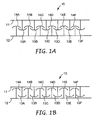
- FIG. 1A and 1B are cross-sectional side views of a fastening structure 10 used in an embodiment of the invention.
- a top layer 11 includes a set of fastening elements 13A-13F (hereafter fastening elements 13), and a bottom layer 12 includes another set of fastening elements 14A-14F (hereafter fastening elements 14).
- a portion of one of the layers 11, 12 functions as a light guide.
- the portion that functions as a light guide may comprise one of the layers 11, 12 in its entirety, both layers in their entireties, or part of one or both layers.
- decorative or functional lighting can be provided to the fastening structure 10 without adding additional light guiding components.
- the fastening elements 13, 14 have sufficient rigidity to allow top layer 11 and bottom layer 12 to be securely fastened to one another.
- the fastening elements 13, 14 are subject to a wide variety of shapes and sizes.
- fastening elements 13, 14 comprise hook-like elements that engage one another in an interlocking arrangement.
- the distance between respective hook-like elements e.g., the distance between fastening element 13A and 13B at the point of attachment to the base may be on the order of 0.25 centimeters, although the invention is not limited in that respect.
- the number of fastening elements 13, 14 that reside on each respective layer 10, 11 may depend on the width of the given layer.
- the lengths of the fastening elements may be the same as the length of the base of a given layer, or may have a length different than the base of the layer, if desired.
- the length of the fastening elements is less than that of the base.
- the fastening structure 10, illustrated in FIGS. 1A and 1B may further include spring-like elements (not shown) such as elastic balls or posts to provide a biasing force that tends to bias the top layer 11 and bottom layer 12 in an open position (as illustrated in FIG. 1A ).
- the layers 11, 12 may be engaged by snapping or sliding them together.
- Various engaged configurations may allow transmission of light between the layers as described in greater detail below. In this manner, a number of lighting effects may be achieved.
- the predetermined distance of travel allowed between the top and bottom layers 11, 12 may be proportional to the size of one or more of the fastening elements 13, 14.
- the height at which the fastening elements 13, 14 protrude from the respective top and bottom layers 11, 12 may be slightly larger than the amount of travel allowed between the top and bottom layers 11, 12.
- the fastening elements 13, 14 may have an element width (the distance between the outermost ends of each fastening elements 13, 14, measured in a plane parallel to the base of the layer 11, 12 associated with the given element) in the range of .01 centimeters to 1 centimeter.
- the distance of travel may be in the range of .01 centimeters to 1 centimeter.
- a distance of travel of less than 3 millimeters, less than 2 millimeters, or even less than 1 millimeter may be desirable for various applications, including applications in switch arrays such as keyboards, keypads or membrane switches.
- the amount of travel can be designed according to particular design specifications.
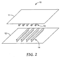
- FIG. 2 is a perspective view of fastening structure 10 in an unengaged state.
- each of the top and bottom layers 11, 12 may comprise films of material extruded according to the desired shape of fastening elements 13, 14.
- one of the layers 11, 12 may comprise more than one type of material, in which case, co-extrusion can be used to form the layer.
- fastening structure 10 can be designed to have a contoured shape.
- the different fastening elements 13, 14 of the different layers 11, 12 may have different sizes to accommodate a contour shape of structure 10 when the top and bottom layers 11, 12 are engaged.
- Part of fastening structure 10 forms a light guide.
- Either top layer 11, bottom layer 12, or both can be extruded using a material that can transmit light via total internal reflection (TIR).
- TIR total internal reflection
- only a portion of top layer 11, bottom layer 12, or both may form a light guide, in which case, a co-extrusion process may be used to form the layer that is only partially a light guide.
- fastening structure 10 can integrate the advantages of a fastener structure, including adhesion capabilities, alignment capabilities and other advantages, with light guide functionality to provide aesthetic, decorative, or functional lighting in any of a number of end applications. Coatings may be applied to fastening structure 10 to improve the TIR through fastening structure 10. In addition, notching or coating techniques may be applied to extract light according to a desired lighting effect.
- FIG. 3 is a cross-sectional side view of two fastening elements.
- the fastening elements may take other forms. If the fastening elements have a hook-like shape, they may include a stem 16A, 16B that attaches hook 18A, 18B to base 17. Distance (X) between stems 18A and 18B may be on the order of 0.25 centimeters although the invention is not necessarily limited in that respect.
- the height (Y) of fastening elements may be in the range of .01 centimeters to I centimeter although the invention is not necessarily limited in that respect.
- the fastening element width (Z) may be in the range of .01 centimeters to 1 centimeter although the invention is not necessarily limited in that respect.
- These shapes and sizes are exemplary for applications in switch arrays. For other applications, the shapes and sizes may be different. For example, sizes larger than those outlined above, by a factor of 10 may be useful for various other applications. Smaller sizes may also be implemented.
- FIGS. 4-6 are cross-sectional side views of a light guide fastening structure and light source positioned to illuminate the light guide fastening structure.
- Light source 40 may comprise any type of light source including an incandescent light source or a fluorescent light source. In many cases, light source 40 may comprise a semiconductor light source such as a light emitting diode (LED). Light source 40 may be positioned adjacent light guide fastening structure 10 so that light guides that form structure 10 can be illuminated to provide the desired lighting effect.
- FIGS. 4-6 illustrate three example configurations for positioning a light source 40 to illuminate light guide fastening structure 10, the configurations of FIGS. 4-6 are exemplary. Other configurations may also exist.
- emission features may comprise surface topography features such as notches, depressions or protrusions, or may comprise material property features such as coatings or other material properties.
- one or more optical elements may be used to improve the transfer of light from light source 40 to light guide fastening structure 10.
- lens 50 may be positioned between light source 40 and light guide fastening structure 10 to adequately condition the light prior to being transmitted through light guide fastening structure 10 via total internal reflection (TIR).
- TIR total internal reflection
- Lens 50 may represent one or more optical elements, or possibly a more complex optical system for improving illumination of light guide fastening structure 10.
- each light source 40A, 40B may have a lens 50A, 50B or a more complex optical system for improving illumination of light guide fastening structure 10.
- the light sources may be chosen so that top and bottom layers are illuminated differently, e.g., with different colors, different intensities, or different temporal on/off (flashing) patterns.
- different light sources may also be used to achieve various lighting effects such as additive color effects and on-off light switching as described in greater detail below.
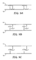
- FIGS. 9A-9C illustrate light guide fastening structure 10 with top layer 11 and bottom layer 12 respectively positioned relative to one another in three possible configurations.
- FIG. 9A illustrates a depressed configuration in which the fastening elements of each layer 11, 12 are in intimate contact with the base of the other layer.
- FIG. 9B illustrates a partially depressed configuration in which the fastening elements of layers 11, 12 are not in intimate contact with the other layer.
- FIG. 9C illustrates a non-depressed configuration in which fastening elements of layers 11, 12 are in intimate contact with one another.
- different lighting effects can be presented depending upon the current configuration of layers 11, 12 relative to one another. For example, if only one of the layers is illuminated by a light source, light may be transferred to the other layer when the layers are in intimate contact ( FIGS. 9A and 9C ). The amount of light transfer between the layers may also be different for the different intimate contact configurations of FIG. 9A and 9C .
- the shapes of the fastening elements may be designed to improve or enhance light transfer between the layers 11, 12 for one or more of the intimate contact configurations.
- both layers 11, 12 are illuminated by a light source
- additive color effects may be achieved.
- the lighting effect may become more intense in certain locations when the layers 11, 12 are in intimate contact.
- the different layers may be illuminated by different colored light sources.
- intimate contact between layers 11 and 12 may cause the light being transmitted in the different layers to combine in an additive manner.
- layer 11 is illuminated with red light
- layer 12 is illuminated with green light
- the layers may appear yellow when they come in intimate contact.
- the red and green light combine in an additive manner to yield yellow light.
- the invention can exploit any of a wide variety of additive color phenomenon to achieve the desired illumination effect in light guide fastening structure 10.
- the shapes of the fastening elements may be designed to improve or enhance light transfer between the layers 11, 12 for one or more of the intimate contact configurations.
- various emission techniques using notches or coating, for example, can be applied to the top or bottom layers 11, 12 to cause light to be emitted from the layers in a controlled or random manner.
- FIG. 10 is a cross-sectional side view of a light guide fastening structure being used as part of a switch array.
- top layer 11 of light guide fastening structure includes a number of distinct top layer sections 11A and 11B.
- Each top layer section 11A, 11B is mechanically engaged with bottom layer 12 via sets of fastening elements.
- Bottom layer 12 may be formed with holes 91A, 91B and springs such as dome springs 93A and 93B may protrude through holes 91A, 91B to bias the top layer sections 11A, 11B away from bottom layer 12.
- dome springs 93A and 93B may bias the top layer sections 11A and 11B by an amount sufficient to place the fastening elements of top layer sections into intimate contact with the fastening elements of bottom layer 12 (as illustrated in FIG. 9C ). As illustrated, the dome springs 93A and 93B may abut the fastening elements of the top layer sections 11A and 11B. Alternatively the fastening elements of top layer sections 11 A and 11B may be removed in the area corresponding to dome springs 93A and 93B, in which case the dome springs 93A and 93B may abut the base of top layer sections 11A and 11B.
- a light source 40 may be positioned to illuminate bottom layer 12, or possibly to illuminate one or more of the top layer sections 11A or 11B. If bottom layer 12 is illuminated, the top layer sections 11A, 11B may also be illuminated via light transmission between the bottom layer 12 and each top layer section 11A, 11B.
- a user may actuate a key of the switch array, for example, causing top layer section 11A to press dome spring 93A. Upon pressing the key, the intimate contact between top layer section 11A and bottom layer 12 is discontinued (as illustrated in FIG. 9B ). In that case, the key may change from an illuminated state to a non-illuminated state.
- top layer section 11A and bottom layer may come back into intimate contact (as illustrated in FIG. 9A ).
- the key may be re-illuminated.
- a visual indication of key actuation may be presented to a user upon depressing a key.
- the key may blink-off momentarily when the user presses the key causing intimate contact between top layer section 11A and bottom layer 12 to be discontinued and then reestablished.
- the same effect may occur when the user releases the key.
- light guide fastening structure 10 may be designed to turn either off or on, and remain in the off or on state when a key is depressed.
- additive color affects may be achieved as described above.
- top and bottom layers 11, 12 may provide a number of advantages in addition to the lighting effect.
- engaged top and bottom layers 11, 12 can provide resistance to rocking of individual keys, and may ensure that individual keys are held in place and properly aligned with individual dome spring elements.
- top and bottom layers 11, 12 can function as alignment structures for individual keys of a switch array.
- the layers 11, 12 can be fabricated at relatively low cost by extrusion or injection molding. Moreover, assembly of switch arrays can be simplified significantly by replacing discrete alignment structures with top and bottom layers 11, 12. The top and bottom layers 11, 12 can be engaged simply by sliding or snapping then together such that fastening elements (for example having hook-like configurations) overlap one another to provide an interlocking arrangement. Machining of mounting brackets for alignment structures can be avoided. Also, the use of fastening structure 10 may enable the realization of thinner switch arrays by reducing the amount of key travel and reducing the number of layers in the switch array. Moreover, the fastening structure 10 as described herein may provide a hermetic barrier or a partial hermetic barrier between the environment and sensors of a switch array.
- layers 11, 12 may provide additional design freedoms to the design of switch arrays.
- a switch array may not need molding to hold the keys in place.
- the shape and layout of the keys can be improved both functionally and/or aesthetically.
- adjacent keys may not need to be separated by molding which can be particularly useful in switch arrays that form part of handheld devices such as cellular radio telephones and handheld computers.
- molding can be eliminated, more space may be dedicated to the keys themselves.
- decorative or functional lighting effects can be implemented as outlined above.
- FIG. 11 is a perspective view of a light guide fastening structure 10 including a bottom layer 12 and a top layer including a plurality of top layer sections 11A-11H.
- Bottom layer 12 can be engaged with each top layer section 11A-11H as described above.
- Bottom layer 12 is formed with holes 91A-91H for aligning with spring elements (not shown) of a switch array.
- holes 91 may be sized in the range of 0.1 to 2.0 square centimeters although the invention is not necessarily limited in that respect.
- holes 91 are square shaped with a surface area of approximately 0.635 square centimeters.
- Each top layer section 11A-11H may cover one of the holes 91A-91H when the layers are engaged.
- the top and bottom layers 11, 12 can be engaged simply by sliding or snapping the top layer sections 11A-11H onto the bottom layer 12.
- top layer sections 11A-11H may function as the keys that are depressed by a user. In this manner, thinner switch arrays, and/or switch arrays having fewer elements can be realized. Alternatively, additional keycaps (not shown) may be attached to the respective top layer sections to be depressed by a user.
- a membrane cover may cover the light guide fastening structure. The membrane cover may be transparent or partially transparent so that the lighting effects described above can be viewed through the membrane cover.
- top layer sections 11A-11H may be desirable to prevent lateral movement of top layer sections 11A-11H relative to bottom layer 12 when the layers are engaged.
- One way to achieve this is to attach the top layer sections 11A-11H to dome spring elements via an adhesive or other suitable attachment means.
- Another way to prevent lateral movement of top layer sections 11A-11H relative to bottom layer 12 is to form regions (not shown) in bottom layer 12.
- a region may define an area for placement of a top layer section 11A-11H to limit the lateral motion of that top layer section 11A-11H relative to bottom layer 12 when the layers are engaged.
- the fastening elements of bottom layer 12 may be heat sealed or crushed by a die in selected places to form the regions. Regions could be created in bottom layer 12 to define the area for placement of each top layer section 11A-11H.
- FIGS. 12 and 13 illustrate another embodiment, implementing a light guide fastening structure in the form of a bottom layer 12 and a single top layer 11 having rigid elements 113 and elastic regions 115.
- FIG. 12 is a cross sectional view. As shown, bottom layer 12 is engaged with a top layer 11. Bottom layer 12 is formed with holes 91A and 91B for aligning with spring elements 93A and 93B.
- Top layer 11 includes rigid elements 113A and 113B and an elastic region 115.
- rigid elements 113A and 113B may function as the keys that are depressed by a user. Alternatively, additional keycaps (not shown) may be attached to the respective rigid elements 113A and 113B.
- FIG. 13 is a perspective view of an unengaged light guide fastening structure in the form of a bottom layer 12 and a top layer 11 according to an embodiment of the invention.
- the bottom layer 12 is formed with holes 91A-91H for aligning with spring elements (not shown).
- Top layer 11 includes rigid elements 113A-113H and one or more elastic regions 115 between the respective rigid elements 113A-113H. Each rigid element 113A-113H may cover one of the holes 91A-91H when the layers are engaged.
- the layers can be engaged simply by sliding or snapping the top layer 11 and the bottom layer 12 together.
- a substantially transparent light guide material such as a transparent polymer can be fed into a single screw extruder (supplied by Davis Standard Corporation of Pawcatuck Connecticut) having a diameter of approximately 6.35 centimeters (2.5 inches), a length/diameter ratio of 24/1, and a temperature profile that steadily increases from approximately 175-232 degrees Celsius (350-450 degrees Fahrenheit).
- Suitable materials may include polymeric materials such as acrylic, polycarbonate, polyester, polystyrene, styrene acrylonitrile, styrenic block copolymers, acrylonitrile butadiene styrene, polyvinyl chloride, cellulossics, polyamide nylon, polysulfone, polyether sulfone, polyphenyl sulfone, polyethylene, ethylene vinyl acetate, ethylene methylacrylic acid, polypropylene, polybutylene, polyurethane, polymethylpentene, silicone plastics, fluoroplastics, or another suitable clarified material.
- polymeric materials such as acrylic, polycarbonate, polyester, polystyrene, styrene acrylonitrile, styrenic block copolymers, acrylonitrile butadiene styrene, polyvinyl chloride, cellulossics, polyamide nylon, polysulfone, polyether
- the substantially transparent material is polypropylene
- it can be continuously discharged at a pressure of at least 690,000 Pascals (100 pounds per square inch) through a necktube heated to approximately 232 degrees Celsius (450 degrees Fahrenheit) and into an approximately 20-centimeter wide (8-inch wide) MasterFlex LD-40 film die (supplied by Production Components of Eau Claire, Wisconsin), maintained at a temperature of approximately 232 degrees Celsius (450 degrees Fahrenheit).
- the die may have a die lip configured to form a film having fastening elements such as elements forming a self-mating profile as shown in Figures 1A and 1B .
- the polypropylene film can be extruded from the die and drop-cast at about 3 meters/minute (10 feet/minute) into a quench tank maintained at 10-21 degrees Celsius (50-70 degrees Fahrenheit) for a residence time of at least 10 seconds.
- the quench medium may be water with 0.1-1.0% by weight of a surfactant, Ethoxy CO-40 (a polyoxyethylene caster oil available from Ethox Chemicals, LLC of Greenville, South Carolina), to increase wet-out of hydrophobic polyolefin materials.
- the quenched film can then be air-dried and collected in 91-137 meter rolls (100-150 yard rolls).
- the film may have a uniform base film caliper of approximately 0.0356 +/- 0.005 centimeters (0.014 +/- 0.002 inches), a fastening elements width (the distance between the outermost ends of the fastening elements, measured in a plane parallel to the base of the film) of about 0.1524 +/- 0.005 centimeters (0.060 +/- 0.002 inches).
- the film may have an extruded basis weight of approximately 700 grams/square meter. The vertical travel permitted may be approximately 0.094 centimeters (0.037 inches).
- the extruded films can be annealed to flatten the base sheet by passage over a smooth cast roll maintained at approximately 93 degrees Celsius (200 degrees Fahrenheit), and then wound onto 15.24 centimeter cores (6 inch cores) to minimize web-curl.
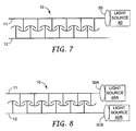
- FIG. 14 is an exploded block diagram of two switches of a membrane switch according to an embodiment of the invention.
- a membrane switch may include a support substrate 131 to provide mechanical stability.
- An electronic membrane 132 may reside on top of the support substrate 131.
- the electronic membrane may include a plurality of sensors that generate signals in response to an applied physical force.
- Dome springs 93 may reside on top the electronic membrane 132.
- the dome springs may be individual dome springs or may be connected to form an array.
- the dome springs may be metal dome springs or may be formed of a polymeric material such as polyester.
- Bottom layer 12 is formed with holes 91A-91B for aligning with dome springs 93A and 93B.
- a top layer 11 defines top layer sections 11A and 11B that correspond to the holes 91A and 91B in bottom layer 12. In other words, each top layer section 11A and 11B may cover one of the holes 91A and 91B when the top and bottom layers 11, 12 are engaged. Dome springs 93A and 93B can bias top layer sections 11A and 11B away from bottom layer 12. When a physical force is applied to one of the top layer sections 11A or 11B, the force can cause depression of the corresponding dome spring, which in turn causes actuation of a sensor within electronic membrane 132.
- Membrane cover 135 can cover the top and bottom layers 11, 12.
- a light source may illuminate the bottom layer 12 and/or one or more of the top layer sections 11A, 11B as outlined above.
- membrane cover 135 may be transparent or partially transparent so that user can see the lighting effects through the membrane cover.
- top layer sections 11A and 11B may comprise keys without the additional membrane cover 135, or alternatively key caps may be added in addition to or instead of membrane cover 135. In that case, the light guide functionality may be used to create lighting effects between the keys.
- top layer 11 and bottom layer 12 By positioning top layer 11 and bottom layer 12 above dome spring elements 93, stiffening of the area associated with each switch can be achieved. More generally, any form of a stiffening agent can be provided above dome spring elements 93 in accordance with embodiments of the invention. Stiffening the area above the dome spring elements 93 can improve switch arrays, particularly membrane switches, by providing a large rigid area for key actuation. In addition, a larger "sweet spot" may be achieved. Furthermore, the need for membrane cover 135 can be avoided for some embodiments. If membrane cover 135 is used, embossing of the membrane cover 135 can be avoided when a stiffening agent such as top layer 11 is positioned above the area associated with a switch.
- the fastening structure including a top layer engaged with a bottom layer as described above may provide design freedoms to a switch array designer. Indeed, compared to conventional switch array configurations, the alignment elements described herein may allow a larger number of keys to be realized in the same amount of area, and can allow the keys to be placed more closely together by eliminating the molding or frame that covers the keys. In addition, as described above, the thickness of switch arrays may be reduced by implementing the fastening structure. Moreover, the need for additional keycaps can be eliminated.
- the fastening structure may also provide alignment advantages including facilitating a larger useful contact area for the key, e.g., a larger "sweet spot," and providing resistance to key rocking.
- the fastening structure may form a light guide that can provide functional or decorative lighting to the switch array as outlined above.
- the fastening structure can form chambers around dome spring elements to enhance audible indication of key actuation.
- the fastening structure as described herein can improve or enhance audible sounds caused by the actuation of dome springs.
- actuation of the key may be accompanied by a tactile feel, a more noticeable audible indication, and/or visual effects.
- the fastening structure as described herein may provide a hermetic barrier or a partial hermetic barrier between the environment and sensors of a switch array. In these ways, the fastening structure may be used to improve switch arrays.
- FIG. 15 illustrates an added embodiment of a switch array.
- the switch array may include a support substrate 131 to provide mechanical stability, and an electronic membrane 132 may reside on top of the support substrate 131.
- the electronic membrane may include a plurality of sensors that generate signals in response to an applied physical force.
- An array of connected dome springs 150 may reside on top of the electronic membrane 132.
- the dome springs 151A and 151B within the array 150 may be connected by a channel 152 as further described in co-pending and commonly assigned United States Patent application number 09/848,458 , which is hereby incorporated by reference in its entirety.
- Bottom layer 12 is formed with holes 91A-91B for aligning with dome springs 151A and 151B, and a top layer 11 defines top layer sections 11A and 11B that correspond to the holes 91 A and 91B in bottom layer 12.
- the array of dome spring elements 150 comprises a light guide.
- the array of dome spring elements 150 can be formed of a material that transmits light via total internal reflection (TIR).
- TIR total internal reflection
- One or more light emission features may be added to the array of dome spring elements 150 to cause light to be emitted in a controlled or random manner.
- channels 152 may enhance the lighting effects.
- Light source 40C can be used to transmit light through the array of dome spring elements 150 via total internal reflection. If desired, one or more additional light sources 40A and 40B can be used to transmit light through top layer 11 and/or bottom layer 12 as outlined above. By illuminating the array of dome spring elements 150, unique lighting of a switch array may be achieved. Light may be transmitted through the various components that comprise light guides, such as one or more of top layer 11, bottom layer 12 and the array of dome spring elements 150. In some cases different colors, different intensities, or different temporal on/off (flashing) patterns can be used. Also, the different light sources may also be used to achieve various lighting effects such as additive color effects and on-off light switching.
- Exemplary implementations of the different embodiments of the invention within switch arrays may include implementations within membrane switches, keypads or keyboards.
- the invention may be implemented to form part of handled computer devices such as palm computers or cellular radio telephones, laptop or desktop keyboards, switch arrays on an instrument panel of an aircraft, watercraft or motor vehicle, or switch arrays in appliances, musical instruments or any other application where switches are used.
- fastening structure may be used in other applications unrelated to switch arrays.
- the fastening structure may be used in any application in which both fastening functionality and light guide functionality are desired. Accordingly, the invention is not limited to the exemplary description of switch array embodiments, but is more broadly envisioned as providing useful advantages in any number of a wide variety of applications.
- extrusion profile-extrusion
- injection molding compression molding
- thermoforming rapid prototyping
- cast and cure embossing
- embossing or other processes
- more complex extrusion processes can be used to form light guide material as part of various layers of a fastening structure.
- inclusion co-extrusion, multi-layer extrusion or micro-layer-multi-layer extrusion may be used to include or embed light guiding materials within other materials to realize light guide fastening structures.
- Inclusion co-extrusion may be useful, for example, to embed glass, polymeric light guiding fibers or high birefringence materials within another material.
- Additives, such as strengthening agents, colorants, or the like may also be added. Accordingly, other implementations and embodiments are within the scope of the following claims.
Landscapes
- Physics & Mathematics (AREA)
- General Physics & Mathematics (AREA)
- Optics & Photonics (AREA)
- Push-Button Switches (AREA)
- Planar Illumination Modules (AREA)
- Illuminated Signs And Luminous Advertising (AREA)
- Non-Portable Lighting Devices Or Systems Thereof (AREA)
- Light Guides In General And Applications Therefor (AREA)
- Revetment (AREA)
Applications Claiming Priority (3)
| Application Number | Priority Date | Filing Date | Title |
|---|---|---|---|
| US10/107,655 US6827459B2 (en) | 2002-03-27 | 2002-03-27 | Lighted fastening structure |
| US107655 | 2002-03-27 | ||
| PCT/US2003/002160 WO2003083531A1 (en) | 2002-03-27 | 2003-01-23 | Interlocking profiled fastening foils used as waveguides for illumination purposes |
Publications (2)
| Publication Number | Publication Date |
|---|---|
| EP1488260A1 EP1488260A1 (en) | 2004-12-22 |
| EP1488260B1 true EP1488260B1 (en) | 2008-07-30 |
Family
ID=28452684
Family Applications (1)
| Application Number | Title | Priority Date | Filing Date |
|---|---|---|---|
| EP03704001A Expired - Lifetime EP1488260B1 (en) | 2002-03-27 | 2003-01-23 | Interlocking profiled fastening foils used as waveguides for illumination purposes |
Country Status (10)
| Country | Link |
|---|---|
| US (1) | US6827459B2 (zh) |
| EP (1) | EP1488260B1 (zh) |
| JP (1) | JP2005521896A (zh) |
| KR (1) | KR20040101354A (zh) |
| CN (1) | CN1317571C (zh) |
| AT (1) | ATE403170T1 (zh) |
| AU (1) | AU2003205323B2 (zh) |
| BR (1) | BR0308404A (zh) |
| DE (1) | DE60322519D1 (zh) |
| WO (1) | WO2003083531A1 (zh) |
Families Citing this family (8)
| Publication number | Priority date | Publication date | Assignee | Title |
|---|---|---|---|---|
| EP1667182A1 (en) * | 2004-12-01 | 2006-06-07 | IEE INTERNATIONAL ELECTRONICS & ENGINEERING S.A. | Foil-type switching element with enhanced carrier foil |
| TWI272412B (en) * | 2004-12-27 | 2007-02-01 | Benq Corp | Light guiding system |
| KR100744283B1 (ko) | 2005-12-05 | 2007-07-30 | 삼성전자주식회사 | 키 패드와 그 제작 방법 |
| CN101459004B (zh) * | 2007-12-14 | 2011-02-09 | 深圳富泰宏精密工业有限公司 | 电子装置的按键面板结构及制造该按键面板结构的方法 |
| CN102555136B (zh) * | 2010-12-29 | 2017-02-22 | 广东天安新材料股份有限公司 | 一种高透明聚丙烯压延片材的制作方法 |
| JP5796167B2 (ja) * | 2011-06-07 | 2015-10-21 | パナソニックIpマネジメント株式会社 | 照明システム |
| US8875356B2 (en) | 2011-10-06 | 2014-11-04 | Intercontinental Great Brands Llc | Mechanical and adhesive based reclosable fasteners |
| FR3027775B1 (fr) * | 2014-10-31 | 2016-11-11 | Aplix Sa | Dispositif de fermeture a crochets dans crochets a effet sensoriel |
Family Cites Families (54)
| Publication number | Priority date | Publication date | Assignee | Title |
|---|---|---|---|---|
| US3266113A (en) | 1963-10-07 | 1966-08-16 | Minnesota Mining & Mfg | Interreacting articles |
| US3879835A (en) | 1972-10-19 | 1975-04-29 | George C Brumlik | Method of making multi element self-gripping device having cooperating gripping elements |
| US4290832A (en) | 1976-08-13 | 1981-09-22 | Minnesota Mining And Manufacturing Company | Method for making fasteners |
| US4109118A (en) | 1976-09-01 | 1978-08-22 | Victor Kley | Keyswitch pad |
| US4249044A (en) | 1979-04-23 | 1981-02-03 | Oak Industries, Inc. | Membrane switch with means for preventing contamination of the interior thereof |
| JPS575222A (en) | 1980-06-10 | 1982-01-12 | Nippon Mektron Kk | Panel keyboard |
| DE3218404A1 (de) | 1982-05-15 | 1983-11-17 | Wolfgang Schulte | Tastenfeld fuer eine gedruckte schaltung |
| JPS59101725A (ja) | 1982-11-30 | 1984-06-12 | 日本メクトロン株式会社 | キ−ボ−ドスイツチ |
| US4500758A (en) | 1983-07-05 | 1985-02-19 | Hewlett-Packard Company | Keyboard switch assembly having sensory feedback |
| US4862499A (en) | 1987-09-04 | 1989-08-29 | Phillips & Brooks, Inc. | Deformable membrane keypad assembly for public telephones |
| US4894060A (en) | 1988-01-11 | 1990-01-16 | Minnesota Mining And Manufacturing Company | Disposable diaper with improved hook fastener portion |
| FR2636683B2 (fr) | 1988-02-26 | 1990-12-28 | Berger Michel | Systeme d'assemblage par accrochage comportant des elements d'accrochage formes par des nervures curvilignes pourvues de levres elastiquement deformables |
| US4981336A (en) * | 1988-06-24 | 1991-01-01 | Paul Mohan | Reversible high density optical fiber connector apparatus |
| US5083240A (en) * | 1989-08-24 | 1992-01-21 | Technophone Limited | Light guide |
| US5130897A (en) * | 1991-10-31 | 1992-07-14 | At&T Bell Laboratories | Light guide for a telephone dial |
| US5235731A (en) | 1992-03-26 | 1993-08-17 | Kuraray Co., Ltd. | Molded-resin separable fastener and fastening system utilizing the same |
| JP3392887B2 (ja) | 1992-10-16 | 2003-03-31 | ミネソタ マイニング アンド マニュファクチャリング カンパニー | 相互係合式ファスナー |
| US5459461A (en) | 1993-07-29 | 1995-10-17 | Crowley; Robert J. | Inflatable keyboard |
| US5396687A (en) * | 1993-11-12 | 1995-03-14 | Osterman; Eric F. | Mechanical fastener |
| FI95177C (fi) | 1994-01-10 | 1995-12-27 | Nokia Mobile Phones Ltd | Elektronisen laitteen valaistulla valintanäppäimistöllä varustettu etupaneeli |
| US5505747A (en) | 1994-01-13 | 1996-04-09 | Minnesota Mining And Manufacturing Company | Method of making an abrasive article |
| US5514843A (en) | 1994-03-23 | 1996-05-07 | Wilfong; James A. | Pressure-compensated key switch |
| US5457297A (en) | 1994-04-20 | 1995-10-10 | Chen; Pao-Chin | Computer keyboard key switch |
| JP3103833B2 (ja) * | 1994-08-10 | 2000-10-30 | 信越ポリマー株式会社 | 照光式押釦スイッチ装置 |
| US5990772A (en) | 1995-06-02 | 1999-11-23 | Duraswitch Industries, Inc. | Pushbutton switch with magnetically coupled armature |
| US5975711A (en) * | 1995-06-27 | 1999-11-02 | Lumitex, Inc. | Integrated display panel assemblies |
| JPH0950728A (ja) | 1995-08-07 | 1997-02-18 | Fuji Polymertech Kk | 照光式スイッチ |
| DE19608773C2 (de) | 1996-03-07 | 1998-11-26 | Preh Elektro Feinmechanik | Schaltmatte |
| US5630501A (en) | 1996-04-12 | 1997-05-20 | Shin Jiuh Corp. | Computer key |
| US5760351A (en) | 1996-04-18 | 1998-06-02 | Chicony Electronics Co., Ltd. | Rubber cone layer of a keyboard |
| US5812116A (en) | 1996-05-30 | 1998-09-22 | Texas Instruments Incorporated | Low profile keyboard |
| JPH1064361A (ja) | 1996-08-21 | 1998-03-06 | Alps Electric Co Ltd | キーボード装置 |
| US5797482A (en) | 1996-11-25 | 1998-08-25 | Metro-Mark, Inc. | Electroluminescent keypad |
| US5742242A (en) | 1996-12-19 | 1998-04-21 | Compaq Computer Corporation | Keyboard using pressurized fluid to generate key stroke characteristics |
| SE513069C2 (sv) | 1997-03-03 | 2000-07-03 | Ericsson Telefon Ab L M | Skydd mot elektrostatisk urladdning i en portabel kommunikationsapparat |
| US5879088A (en) | 1997-11-24 | 1999-03-09 | Key Tronic Corporation | Computer keyboard with adjustable force keystroke feature using air pressure |
| ITTO980212A1 (it) | 1998-03-12 | 1999-09-12 | Proto El Srl | Tastiera a tenuta ermetica |
| DE19819693B4 (de) | 1998-05-02 | 2004-10-21 | Berker Gmbh & Co. Kg | Federschaltelement mit taktiler Rückmeldung |
| JP2000151772A (ja) | 1998-11-12 | 2000-05-30 | Matsushita Electric Ind Co Ltd | 携帯端末装置 |
| TW446616B (en) | 1999-01-27 | 2001-07-21 | Taisei Plastics Co Ltd | Control panel having sheet-formed pushbutton unit and method of producing the same |
| US6178619B1 (en) | 1999-02-12 | 2001-01-30 | Fu-Chen Tai | Assembling method for key board |
| US6064019A (en) | 1999-04-27 | 2000-05-16 | Buchan; Brian D. | Resilient switch cover with integral actuator button |
| JP3204951B2 (ja) | 1999-05-24 | 2001-09-04 | ポリマテック株式会社 | キーシート及びその製造方法 |
| US6137072A (en) | 1999-05-26 | 2000-10-24 | Ferro Corporation | Control panel |
| JP3311707B2 (ja) | 1999-06-17 | 2002-08-05 | エスエムケイ株式会社 | メンブレンスイッチ |
| JP2001014974A (ja) * | 1999-06-29 | 2001-01-19 | Alps Electric Co Ltd | 可動接点付きシート及びシートスイッチ |
| WO2001058780A1 (en) | 2000-02-10 | 2001-08-16 | 3M Innovative Properties Company | Self-mating reclosable binding strap and fastener |
| US6300582B1 (en) | 2000-02-11 | 2001-10-09 | Silitek Corporation | Dustproof and droplet-proof keyswitch |
| DE20009377U1 (de) | 2000-05-25 | 2000-08-17 | Chicony Electronics Co | Elastischer Bewegungskontaktkörper zur leichten Montage an eine feuchtigkeitsgeschützte Tastatur |
| US6252184B1 (en) | 2000-05-25 | 2001-06-26 | Chicony Electronics Co., Ltd. | Droplet proof keyboard for notebook computer |
| DE20016887U1 (de) | 2000-09-29 | 2001-01-11 | Fang Jason | Verbessertes Membrankeyboard |
| US7091952B2 (en) | 2001-05-03 | 2006-08-15 | 3M Innovative Properties Company | Liquid proof switch array |
| US6690360B2 (en) | 2001-05-03 | 2004-02-10 | 3M Innovative Properties Company | Liquid proof switch array |
| US6575586B1 (en) * | 2002-01-29 | 2003-06-10 | Behavior Tech Computer Corporation | Lighting unit |
-
2002
- 2002-03-27 US US10/107,655 patent/US6827459B2/en not_active Expired - Fee Related
-
2003
- 2003-01-23 EP EP03704001A patent/EP1488260B1/en not_active Expired - Lifetime
- 2003-01-23 JP JP2003580908A patent/JP2005521896A/ja not_active Withdrawn
- 2003-01-23 AT AT03704001T patent/ATE403170T1/de not_active IP Right Cessation
- 2003-01-23 BR BR0308404-3A patent/BR0308404A/pt not_active IP Right Cessation
- 2003-01-23 WO PCT/US2003/002160 patent/WO2003083531A1/en active Application Filing
- 2003-01-23 DE DE60322519T patent/DE60322519D1/de not_active Expired - Fee Related
- 2003-01-23 KR KR10-2004-7015070A patent/KR20040101354A/ko not_active Application Discontinuation
- 2003-01-23 AU AU2003205323A patent/AU2003205323B2/en not_active Expired - Fee Related
- 2003-01-23 CN CNB038070324A patent/CN1317571C/zh not_active Expired - Fee Related
Also Published As
| Publication number | Publication date |
|---|---|
| AU2003205323A1 (en) | 2003-10-13 |
| DE60322519D1 (de) | 2008-09-11 |
| WO2003083531A1 (en) | 2003-10-09 |
| US6827459B2 (en) | 2004-12-07 |
| JP2005521896A (ja) | 2005-07-21 |
| EP1488260A1 (en) | 2004-12-22 |
| CN1317571C (zh) | 2007-05-23 |
| ATE403170T1 (de) | 2008-08-15 |
| CN1643410A (zh) | 2005-07-20 |
| KR20040101354A (ko) | 2004-12-02 |
| AU2003205323B2 (en) | 2008-04-24 |
| BR0308404A (pt) | 2005-02-09 |
| US20030184991A1 (en) | 2003-10-02 |
Similar Documents
| Publication | Publication Date | Title |
|---|---|---|
| EP2053621A1 (en) | Key sheet, key unit having it, and key sheet manufacturing method | |
| EP1782169B1 (en) | Thin keypad assemblies and components for electronics devices and methods | |
| EP1962314B1 (en) | Light guide sheet and movable contact unit and switch using the same | |
| US8530768B2 (en) | Thin illuminated keyboard | |
| EP1488260B1 (en) | Interlocking profiled fastening foils used as waveguides for illumination purposes | |
| US8350172B2 (en) | Illuminated keyboard | |
| WO1998011576A1 (en) | Electroluminescent backlit keypad | |
| WO2008091868A2 (en) | Dome sheet with light guide for membrane switch | |
| US8411038B2 (en) | Multi-layer integral keypad | |
| KR100752517B1 (ko) | 잉크 인쇄방식 및 측면발광을 이용한 전기전자제품의버튼장치 및 제조방법 | |
| US7718910B2 (en) | Movable contact assembly and switch using the same | |
| US7737375B2 (en) | Key sheet | |
| EP1390960B1 (en) | Liquid proof switch array | |
| EP1386337B1 (en) | Liquid proof switch array | |
| AU2002255931A1 (en) | Liquid proof switch array | |
| EP2494391B1 (en) | Light source and proconductor coupling arrangement | |
| US6740832B2 (en) | Apparatus exhibiting tactile feel | |
| KR100880139B1 (ko) | 키 유닛과 키 유닛의 제조방법 | |
| TWM472236U (zh) | 薄型鍵盤 | |
| JP2005011686A (ja) | 押しボタンスイッチの識別構造 |
Legal Events
| Date | Code | Title | Description |
|---|---|---|---|
| PUAI | Public reference made under article 153(3) epc to a published international application that has entered the european phase |
Free format text: ORIGINAL CODE: 0009012 |
|
| 17P | Request for examination filed |
Effective date: 20041006 |
|
| AK | Designated contracting states |
Kind code of ref document: A1 Designated state(s): AT BE BG CH CY CZ DE DK EE ES FI FR GB GR HU IE IT LI LU MC NL PT SE SI SK TR |
|
| AX | Request for extension of the european patent |
Extension state: AL LT LV MK RO |
|
| 17Q | First examination report despatched |
Effective date: 20041230 |
|
| GRAP | Despatch of communication of intention to grant a patent |
Free format text: ORIGINAL CODE: EPIDOSNIGR1 |
|
| RIC1 | Information provided on ipc code assigned before grant |
Ipc: H01R 13/70 20060101ALI20080128BHEP Ipc: G02B 6/10 20060101AFI20080128BHEP |
|
| GRAS | Grant fee paid |
Free format text: ORIGINAL CODE: EPIDOSNIGR3 |
|
| GRAA | (expected) grant |
Free format text: ORIGINAL CODE: 0009210 |
|
| AK | Designated contracting states |
Kind code of ref document: B1 Designated state(s): AT BE BG CH CY CZ DE DK EE ES FI FR GB GR HU IE IT LI LU MC NL PT SE SI SK TR |
|
| REG | Reference to a national code |
Ref country code: GB Ref legal event code: FG4D |
|
| REG | Reference to a national code |
Ref country code: CH Ref legal event code: EP |
|
| REF | Corresponds to: |
Ref document number: 60322519 Country of ref document: DE Date of ref document: 20080911 Kind code of ref document: P |
|
| REG | Reference to a national code |
Ref country code: IE Ref legal event code: FG4D |
|
| PG25 | Lapsed in a contracting state [announced via postgrant information from national office to epo] |
Ref country code: PT Free format text: LAPSE BECAUSE OF FAILURE TO SUBMIT A TRANSLATION OF THE DESCRIPTION OR TO PAY THE FEE WITHIN THE PRESCRIBED TIME-LIMIT Effective date: 20081230 Ref country code: NL Free format text: LAPSE BECAUSE OF FAILURE TO SUBMIT A TRANSLATION OF THE DESCRIPTION OR TO PAY THE FEE WITHIN THE PRESCRIBED TIME-LIMIT Effective date: 20080730 Ref country code: ES Free format text: LAPSE BECAUSE OF FAILURE TO SUBMIT A TRANSLATION OF THE DESCRIPTION OR TO PAY THE FEE WITHIN THE PRESCRIBED TIME-LIMIT Effective date: 20081110 |
|
| PG25 | Lapsed in a contracting state [announced via postgrant information from national office to epo] |
Ref country code: BG Free format text: LAPSE BECAUSE OF FAILURE TO SUBMIT A TRANSLATION OF THE DESCRIPTION OR TO PAY THE FEE WITHIN THE PRESCRIBED TIME-LIMIT Effective date: 20081030 Ref country code: AT Free format text: LAPSE BECAUSE OF FAILURE TO SUBMIT A TRANSLATION OF THE DESCRIPTION OR TO PAY THE FEE WITHIN THE PRESCRIBED TIME-LIMIT Effective date: 20080730 Ref country code: FI Free format text: LAPSE BECAUSE OF FAILURE TO SUBMIT A TRANSLATION OF THE DESCRIPTION OR TO PAY THE FEE WITHIN THE PRESCRIBED TIME-LIMIT Effective date: 20080730 Ref country code: SI Free format text: LAPSE BECAUSE OF FAILURE TO SUBMIT A TRANSLATION OF THE DESCRIPTION OR TO PAY THE FEE WITHIN THE PRESCRIBED TIME-LIMIT Effective date: 20080730 |
|
| PG25 | Lapsed in a contracting state [announced via postgrant information from national office to epo] |
Ref country code: BE Free format text: LAPSE BECAUSE OF FAILURE TO SUBMIT A TRANSLATION OF THE DESCRIPTION OR TO PAY THE FEE WITHIN THE PRESCRIBED TIME-LIMIT Effective date: 20080730 |
|
| PG25 | Lapsed in a contracting state [announced via postgrant information from national office to epo] |
Ref country code: DK Free format text: LAPSE BECAUSE OF FAILURE TO SUBMIT A TRANSLATION OF THE DESCRIPTION OR TO PAY THE FEE WITHIN THE PRESCRIBED TIME-LIMIT Effective date: 20080730 Ref country code: EE Free format text: LAPSE BECAUSE OF FAILURE TO SUBMIT A TRANSLATION OF THE DESCRIPTION OR TO PAY THE FEE WITHIN THE PRESCRIBED TIME-LIMIT Effective date: 20080730 |
|
| PG25 | Lapsed in a contracting state [announced via postgrant information from national office to epo] |
Ref country code: SK Free format text: LAPSE BECAUSE OF FAILURE TO SUBMIT A TRANSLATION OF THE DESCRIPTION OR TO PAY THE FEE WITHIN THE PRESCRIBED TIME-LIMIT Effective date: 20080730 Ref country code: CZ Free format text: LAPSE BECAUSE OF FAILURE TO SUBMIT A TRANSLATION OF THE DESCRIPTION OR TO PAY THE FEE WITHIN THE PRESCRIBED TIME-LIMIT Effective date: 20080730 |
|
| PLBE | No opposition filed within time limit |
Free format text: ORIGINAL CODE: 0009261 |
|
| STAA | Information on the status of an ep patent application or granted ep patent |
Free format text: STATUS: NO OPPOSITION FILED WITHIN TIME LIMIT |
|
| 26N | No opposition filed |
Effective date: 20090506 |
|
| PG25 | Lapsed in a contracting state [announced via postgrant information from national office to epo] |
Ref country code: IT Free format text: LAPSE BECAUSE OF FAILURE TO SUBMIT A TRANSLATION OF THE DESCRIPTION OR TO PAY THE FEE WITHIN THE PRESCRIBED TIME-LIMIT Effective date: 20080730 Ref country code: MC Free format text: LAPSE BECAUSE OF NON-PAYMENT OF DUE FEES Effective date: 20090131 |
|
| REG | Reference to a national code |
Ref country code: CH Ref legal event code: PL |
|
| GBPC | Gb: european patent ceased through non-payment of renewal fee |
Effective date: 20090123 |
|
| PG25 | Lapsed in a contracting state [announced via postgrant information from national office to epo] |
Ref country code: CH Free format text: LAPSE BECAUSE OF NON-PAYMENT OF DUE FEES Effective date: 20090131 Ref country code: LI Free format text: LAPSE BECAUSE OF NON-PAYMENT OF DUE FEES Effective date: 20090131 Ref country code: DE Free format text: LAPSE BECAUSE OF NON-PAYMENT OF DUE FEES Effective date: 20090801 |
|
| REG | Reference to a national code |
Ref country code: FR Ref legal event code: ST Effective date: 20091030 |
|
| PG25 | Lapsed in a contracting state [announced via postgrant information from national office to epo] |
Ref country code: GB Free format text: LAPSE BECAUSE OF NON-PAYMENT OF DUE FEES Effective date: 20090123 |
|
| PG25 | Lapsed in a contracting state [announced via postgrant information from national office to epo] |
Ref country code: SE Free format text: LAPSE BECAUSE OF FAILURE TO SUBMIT A TRANSLATION OF THE DESCRIPTION OR TO PAY THE FEE WITHIN THE PRESCRIBED TIME-LIMIT Effective date: 20081030 Ref country code: IE Free format text: LAPSE BECAUSE OF NON-PAYMENT OF DUE FEES Effective date: 20090123 |
|
| PG25 | Lapsed in a contracting state [announced via postgrant information from national office to epo] |
Ref country code: FR Free format text: LAPSE BECAUSE OF NON-PAYMENT OF DUE FEES Effective date: 20090202 |
|
| PG25 | Lapsed in a contracting state [announced via postgrant information from national office to epo] |
Ref country code: GR Free format text: LAPSE BECAUSE OF FAILURE TO SUBMIT A TRANSLATION OF THE DESCRIPTION OR TO PAY THE FEE WITHIN THE PRESCRIBED TIME-LIMIT Effective date: 20081031 |
|
| PG25 | Lapsed in a contracting state [announced via postgrant information from national office to epo] |
Ref country code: LU Free format text: LAPSE BECAUSE OF NON-PAYMENT OF DUE FEES Effective date: 20090123 |
|
| PG25 | Lapsed in a contracting state [announced via postgrant information from national office to epo] |
Ref country code: HU Free format text: LAPSE BECAUSE OF FAILURE TO SUBMIT A TRANSLATION OF THE DESCRIPTION OR TO PAY THE FEE WITHIN THE PRESCRIBED TIME-LIMIT Effective date: 20090131 |
|
| PG25 | Lapsed in a contracting state [announced via postgrant information from national office to epo] |
Ref country code: TR Free format text: LAPSE BECAUSE OF FAILURE TO SUBMIT A TRANSLATION OF THE DESCRIPTION OR TO PAY THE FEE WITHIN THE PRESCRIBED TIME-LIMIT Effective date: 20080730 |
|
| PG25 | Lapsed in a contracting state [announced via postgrant information from national office to epo] |
Ref country code: CY Free format text: LAPSE BECAUSE OF FAILURE TO SUBMIT A TRANSLATION OF THE DESCRIPTION OR TO PAY THE FEE WITHIN THE PRESCRIBED TIME-LIMIT Effective date: 20080730 |