EP1487057A1 - Anisotropic conductive sheet and its manufacturing method - Google Patents
Anisotropic conductive sheet and its manufacturing method Download PDFInfo
- Publication number
- EP1487057A1 EP1487057A1 EP03744535A EP03744535A EP1487057A1 EP 1487057 A1 EP1487057 A1 EP 1487057A1 EP 03744535 A EP03744535 A EP 03744535A EP 03744535 A EP03744535 A EP 03744535A EP 1487057 A1 EP1487057 A1 EP 1487057A1
- Authority
- EP
- European Patent Office
- Prior art keywords
- conductive
- sheet
- nonconductive
- anisotropic conductive
- pieces
- Prior art date
- Legal status (The legal status is an assumption and is not a legal conclusion. Google has not performed a legal analysis and makes no representation as to the accuracy of the status listed.)
- Withdrawn
Links
Images


Classifications
-
- H—ELECTRICITY
- H01—ELECTRIC ELEMENTS
- H01R—ELECTRICALLY-CONDUCTIVE CONNECTIONS; STRUCTURAL ASSOCIATIONS OF A PLURALITY OF MUTUALLY-INSULATED ELECTRICAL CONNECTING ELEMENTS; COUPLING DEVICES; CURRENT COLLECTORS
- H01R11/00—Individual connecting elements providing two or more spaced connecting locations for conductive members which are, or may be, thereby interconnected, e.g. end pieces for wires or cables supported by the wire or cable and having means for facilitating electrical connection to some other wire, terminal, or conductive member, blocks of binding posts
- H01R11/01—Individual connecting elements providing two or more spaced connecting locations for conductive members which are, or may be, thereby interconnected, e.g. end pieces for wires or cables supported by the wire or cable and having means for facilitating electrical connection to some other wire, terminal, or conductive member, blocks of binding posts characterised by the form or arrangement of the conductive interconnection between the connecting locations
-
- H—ELECTRICITY
- H01—ELECTRIC ELEMENTS
- H01R—ELECTRICALLY-CONDUCTIVE CONNECTIONS; STRUCTURAL ASSOCIATIONS OF A PLURALITY OF MUTUALLY-INSULATED ELECTRICAL CONNECTING ELEMENTS; COUPLING DEVICES; CURRENT COLLECTORS
- H01R13/00—Details of coupling devices of the kinds covered by groups H01R12/70 or H01R24/00 - H01R33/00
- H01R13/02—Contact members
- H01R13/22—Contacts for co-operating by abutting
- H01R13/24—Contacts for co-operating by abutting resilient; resiliently-mounted
- H01R13/2407—Contacts for co-operating by abutting resilient; resiliently-mounted characterized by the resilient means
- H01R13/2414—Contacts for co-operating by abutting resilient; resiliently-mounted characterized by the resilient means conductive elastomers
-
- H—ELECTRICITY
- H01—ELECTRIC ELEMENTS
- H01R—ELECTRICALLY-CONDUCTIVE CONNECTIONS; STRUCTURAL ASSOCIATIONS OF A PLURALITY OF MUTUALLY-INSULATED ELECTRICAL CONNECTING ELEMENTS; COUPLING DEVICES; CURRENT COLLECTORS
- H01R43/00—Apparatus or processes specially adapted for manufacturing, assembling, maintaining, or repairing of line connectors or current collectors or for joining electric conductors
- H01R43/007—Apparatus or processes specially adapted for manufacturing, assembling, maintaining, or repairing of line connectors or current collectors or for joining electric conductors for elastomeric connecting elements
-
- Y—GENERAL TAGGING OF NEW TECHNOLOGICAL DEVELOPMENTS; GENERAL TAGGING OF CROSS-SECTIONAL TECHNOLOGIES SPANNING OVER SEVERAL SECTIONS OF THE IPC; TECHNICAL SUBJECTS COVERED BY FORMER USPC CROSS-REFERENCE ART COLLECTIONS [XRACs] AND DIGESTS
- Y10—TECHNICAL SUBJECTS COVERED BY FORMER USPC
- Y10T—TECHNICAL SUBJECTS COVERED BY FORMER US CLASSIFICATION
- Y10T428/00—Stock material or miscellaneous articles
- Y10T428/25—Web or sheet containing structurally defined element or component and including a second component containing structurally defined particles
-
- Y—GENERAL TAGGING OF NEW TECHNOLOGICAL DEVELOPMENTS; GENERAL TAGGING OF CROSS-SECTIONAL TECHNOLOGIES SPANNING OVER SEVERAL SECTIONS OF THE IPC; TECHNICAL SUBJECTS COVERED BY FORMER USPC CROSS-REFERENCE ART COLLECTIONS [XRACs] AND DIGESTS
- Y10—TECHNICAL SUBJECTS COVERED BY FORMER USPC
- Y10T—TECHNICAL SUBJECTS COVERED BY FORMER US CLASSIFICATION
- Y10T428/00—Stock material or miscellaneous articles
- Y10T428/26—Web or sheet containing structurally defined element or component, the element or component having a specified physical dimension
Definitions
- This invention relates to an anisotropic conductive sheet which is interposed between a circuit board such as a substrate and various circuit components to conductive paths and to a manufacturing method thereof.
- connection methods thereof are based upon the solder junction technology and the use of anisotropic conductive adhesive.
- anisotropic conductive adhesive There is employed a method of interposing an anisotropic conductive elastomer sheet between the electronic parts (components) and the circuit board to render conductive paths.
- the anisotropic conductive elastomer sheets include sheets having conductivity only in the direction of thickness or conductivity only in the direction of thickness when the sheets are compressed in the direction of thickness. They have such features as accomplishing compact electric connection without using such means as soldering or mechanical fitting, and realizing a soft connection so as to absorb mechanical shocks and distortion. Therefore, they have been extensively used as connectors for achieving electric connection relative to circuit devices such as printed circuit board, leadless chip carrier and liquid crystal panel in the fields of cell phones, electronic calculators, electronic digital clocks, electronic cameras, computers and the like.
- the anisotropic elastomer sheet has heretofore been interposed between a region of electrodes of the circuit device to be tested and a region of testing electrodes of the circuit board for the test in order to achieve electric connection between the tested electrodes formed on at least one surface of the circuit device to be tested and the testing electrodes formed on the surface of the circuit board for the test.
- anisotropic conductive elastomer sheet may be obtained by cutting an anisotropic conductive block in a thin sheet such that the block that is formed integrally with thin metal wires disposed in parallel and insulating material enclosing the metal wires is cut in a direction orthogonal to the direction of the thin metal wires (JP-A-2000-340037).
- anisotropic conductive film with thin metal wires it is difficult to shorten distance between such thin metal wires and to secure anisotropic conductivity with a fine pitch as required by recent highly integrated circuit boards and electronic components. Further, it is likely that thin metal wires are to be buckled with compressive force or the like during the use thereof and easily pulled out after repetitive use so that the anisotropic conductive film may fail to keep its function to a sufficient degree.
- this invention provides an anisotropic conductive sheet having a fine pitch required by the recent highly integrated circuit boards and electronic components, the anisotropic conductive sheet yet keeping high conductivity in the direction of thickness and preventing conductive members such as metals from slipping out.
- an anisotropic conductive sheet in which conductive members are scattered in a nonconductive matrix, wherein the conductive members penetrate in the direction of thickness and conductive auxiliary layers are in contact with the conductive members.
- the present invention provides the following.
- an anisotropic conductive sheet comprises conductive members scattered in the nonconductive matrix, in which the conductive members penetrates the sheet in the thickness direction, wherein the conductive auxiliary layers are in contact with the conductive members.
- the nonconductive matrix is a sheet member made of nonconductive material so as to insulate the scattering conductive pieces in directions contained in the plane of the sheet (directions in X-Y plane) to maintain non-conductivity in the directions contained in the plane of the whole anisotropic conductive sheet.
- the nonconductive matrix is all connected (being continuous) in the anisotropic conductive sheet to form an anisotropic conductive sheet.
- the nonconductive matrix may not have to be continuous.
- the scattered conductive pieces may refer to a condition that one or more conductive pieces made of a conductive material are spread separately from each other in directions contained in the plane of the sheet.
- the scattered conductive pieces made of a conductive material penetrate the anisotropic conductive sheet from the front surface to the back surface may mean that the conductive pieces penetrate the sheet in the thickness direction, may mean that the conductive pieces appear on both front and back surfaces of the anisotropic conductive sheet, or may mean that the sheet has a function for electrically connecting the front and back surfaces.
- the conductive auxiliary layers are in contact with the conductive members may mean that the conductive auxiliary layers are electrically connected to the conductive members.
- the conductive auxiliary layers have conductivity higher than the conductive members. When the electricity flows in parallel (as being parallel-connected), therefore, the electric conductivity of the conductive auxiliary layers become dominant in the entire conductivity.
- the resistance between the front and the back of the sheet becomes low when the conductive auxiliary layers are adhered, and may become equal to the resistance of the conductive auxiliary layers.
- the conductive auxiliary layers that are made of metal material can be called metal layers.
- the metal layer as a whole may be made of metal of a single kind.
- the anisotropic conductive sheet of the present invention expands on a plane, and the feature of the sheet can be described by using X-direction and Y-direction which are two directions in parallel with the plane, and Z-direction orthogonal to X-direction and Y-direction.
- the anisotropic conductive sheet has thickness in Z-direction
- the strip-like member of the striped pattern has a width in Y-direction and extends in X-direction
- the conductive pieces made of conductive material and nonconductive pieces made of nonconductive material are alternately arranged in X-direction.
- the nonconductive strip-like member has width in Y-direction and extends in X-direction.
- the strip-like members having the striped pattern and the nonconductive strip-like members are arranged in Y-direction, and are included in the anisotropic conductive sheet in this state.
- the conductive auxiliary members are arranged among the conductive pieces and the nonconductive pieces while in contact with the conductive pieces.
- Being conductive may mean that the anisotropic conductive sheet of such constitution has sufficiently high conductivity in the conduction direction. It is usually preferable that the resistance among the terminals to be connected is not larger than 100 ⁇ (preferably, not larger than 10 ⁇ and, more preferably not larger than 1 ⁇ ).
- the strip-like member of the striped pattern may be thin and elongated in X-direction such that conductive members and nonconductive members are alternately arranged along X-direction, wherein a striped pattern may appear if the conductive members and the nonconductive members have different colors. In practice, they need not appear in a striped pattern. The alternate arrangement needs not expand over the whole strip-like members in X-direction but may exist in only a portion thereof. Further, "the conductive auxiliary layers being in contact with the conductive members” may stand for the electric connection in the same manner as described above.
- the conductive auxiliary layers comprise the adhesive layers and the conductive layers.
- the adhesive layers may be those for improving the adhesion to the conductive members while the conductive auxiliary layers come in contact with the conductive members.
- the conductive layers of the conductive auxiliary layers have physical and chemical properties which are greatly different from the physical and chemical properties of the conductive members so that the adhesive layers have a function to improve adhesion between them as the adhesive layers have intermediate properties and bond the conductive layer and the conductive member. Therefore, it may be characterized in that the adhesive layers are arranged on the side of the conductive member being in contact with the conductive auxiliary layers comprising the adhesive layers as a constituent element. For example, it may be possible to lower or absorb distortion caused by the different thermal expansion rate.
- the adhesive layer is arranged on the side of the nonconductive matrix while the conductive auxiliary layer is in contact with the nonconductive matrix.
- being in contact with the nonconductive matrix may mean that the conductive auxiliary layers are physically (mechanically) in contact with the nonconductive matrix. This is because the nonconductive matrix is insulative.
- Being arranged on the side of the nonconductive matrix may mean that the adhesive layer is positioned between the conductive layer and the nonconductive matrix.
- the adhesive layer may be a layer to improve the adhesion to the nonconductive matrix while the conductive auxiliary layer is in contact with the nonconductive matrix.
- the conductive layer of the conductive auxiliary layer has physical and chemical properties which are greatly different from the physical and chemical properties of the conductive member so that the adhesive layer can have a function to improve the adhesion between them as the adhesive layer has intermediate properties and bonds the conductive auxiliary layer and the conductive member, Therefore, it may be characterized in that the adhesive layers are arranged on the side of the conductive members which are in contact with the conductive auxiliary layers comprising the adhesive layer as a constituent element. For example, distortion caused by different thermal expansion rate can be lowered or absorbed.
- the adhesive layer comprises a metal oxide or a metal.
- the metal oxide include indium oxide, tin oxide, titanium oxide, a mixture thereof and a compound thereof, and examples of the metal include chromium.
- the adhesive layer comprises indium tin oxide (or indium oxide / tin oxide).
- Indium tin oxide (or indium oxide / tin oxide) is a ceramic material abbreviated as ITO and has high electric conductivity.
- the conductive layer may be made of metal having good conductivity. If the metal has electric conductivity higher than that of the conductive members and if electricity flows in parallel therewith (in a parallel-connected manner), the electric resistance of the metal controls the entire electric resistance.
- the anisotropic conductive sheet of the present invention may be characterized in that the nonconductive matrix comprises a nonconductive elastomer, and the conductive members comprise a conductive elastomer.
- the conductive elastomer stands for an elastomer having electric conductivity and is, usually, an elastomer blended with a conductive material so as to lower the volume resistivity (smaller than, for example, 1 ⁇ -cm).
- butadiene copolymers such as natural rubber, polyisoprene rubber, butadiene/styrene, butadiene / acrylonitrile, butadiene / isobutylene, conjugated diene rubber and hydrogenated compounds thereof; block copolymer rubbers such as styrene/butadiene / diene block copolymer rubber, styrene / isoprene block copolymer, and hydrogenated compounds thereof; and chloroprene copolymer, vinyl chloride / vinyl acetate copolymer, urethane rubber, polyester rubber, epichlorohydrin rubber, ethylene/propylene copolymer rubber, ethylene / propylene/diene copo
- the silicone rubber is preferably used owing to its excellent heat resistance, cold resistance, chemical resistance, aging resistance, electric insulation and safety.
- the elastomer may be blended with a conductive substance like a powder (flakes, small pieces, folls, etc. are allowable) of a metal such as gold, silver, copper, nickel, tungsten, platinum, palladium or any other pure metal, SUS, phosphor bronze or beryllium copper, or a nonmetallic powder (flakes, small pieces, foils, etc. can be utilized) such as carbon powder to obtain a conductive elastomer.
- carbon may include carbon nano-tube and fullerene.
- the nonconductive elastomer stands for elastomer without conductivity or having a very low conductivity, or elastomer having a sufficiently high electric resistance.
- butadiene copolymers such as natural rubber, polyisoprene rubber, butadiene/styrene, butadiene / acrylonitrile, butadiene / isobutylene, conjugated diene rubber and hydrogenated compounds thereof; block copolymer rubbers such as styrene/butadiene / diene block copolymer rubber, styrene / isoprene black copolymer, and hydrogenated compounds thereof; and chloroprene copolymer, vinyl chloride / vinyl acetate copolymer, urethane rubber, polyester rubber, epichlorohydrin rubber, ethylene/propylene copolymer rubber, ethylene/propylene / diene copolymer rubber, soft liquid epoxy rubber, silicone rubber and fluorine-con
- the silicone rubber is preferably used owing to its excellent heat resistance, cold resistance, chemical resistance, aging resistance, electric insulation and safety.
- the nonconductive elastomer usually has high volume resistivity (e.g., not smaller than 1 M ⁇ -cm at 100 V) and is nonconductive.
- a coupling agent may be applied between them.
- the coupling agent is an agent for coupling these members, and may include an adhesive commercially available.
- coupling agents of the types of silane, aluminum and titanate may be utilized. Among them, a silane coupling agent is favorably used.
- the anisotropic conductive sheet of the present invention may be characterized in that the conductive members are protruded as compared to the nonconductive matrix.
- “Protruding” refers to a case where the portion of the conductive member is thicker than the portion of the nonconductive matrix in the thickness direction of the anisotropic sheet, a case where the position of the upper surface of the nonconductive matrix is lower than the position of the upper surface of the conductive member when the anisotropic conductive sheet is horizontally placed, and/or a case where the position of the lower surface of the nonconductive matrix is higher than the position of the lower surface of the conductive member when the anisotropic conductive sheet is horizontally placed.
- the electric contact becomes more reliable to the electronic parts and to the terminals of the substrate. This is because the terminals, first, come in contact with the conductive members as they approach the sheet such that a suitable degree of contact pressure is maintained due to the pushing force to the sheet.
- a method of manufacturing an anisotropic conductive sheet according to the present invention comprises: a step of adhering conductive auxiliary layers on the surface of a conductive sheet (A) made of conductive material to obtain a conductive sheet (A) with the conductive auxiliary layers; a step of alternately laminating the conductive sheet (A) with the conductive auxiliary layers obtained in the step of adhering the layers and a nonconductive sheet (B) to obtain an AB sheet laminate (C); a first step of cutting the AB sheet laminate (C) obtained in the step of obtaining the AB sheet laminate to obtain a zebra-like sheet in a predetermined thickness; a step of alternately laminating the zebra-like sheet obtained in the first cutting step and a nonconductive sheet (D) to obtain a zebra-D (ZD) sheet laminate (E); and a second step of cutting the ZD sheet laminate (E) with a predetermined thickness obtained in the step of obtaining the ZD sheet laminate.
- the conductive sheet (A) may be a sheet member of a single kind or a collection of sheet members of different kinds.
- the conductive sheet (A) may be a collection of sheet members of the same material but having different thicknesses.
- the conductive auxiliary layers may be adhered onto one surface or both surfaces of the sheet members.
- the conductive auxiliary layers can be adhered by any one of the vapor phase method, liquid phase method or solid phase method or by a combination thereof. Among them, the vapor phase is particularly preferred.
- the vapor phase method there can be exemplified PVD such as sputtering method and vacuum evaporation, and CVD.
- the conductive auxiliary layer is constituted by the adhesive layer and the conductive layer, the respective layers may be adhered with the same method or with different methods.
- the conductive sheet (A) with the conductive auxiliary layer and the nonconductive sheet (B) may be the sheet members of a single kind as described above or may be collections of sheet members of different kinds. Alternate stacking may mean that the conductive sheet (A) with the conductive auxiliary layer and the nonconductive sheet (B) are alternately stacked in any order, which, however, does not exclude interposing a third sheet, a film or any other members between the conductive sheet (A) with the conductive auxiliary layer and the nonconductive sheet (B). In the step of stacking the sheet members, further, a coupling agent may be applied among the sheets so that the sheets are coupled together.
- the AB sheet laminate (C) prepared by stacking may be heated in order to promote curing of the sheet members themselves for increasing the coupling among the sheets or for any other purposes.
- the AB sheet laminate (C) can be cut with a blade such as a cemented carbide cutter blade or a ceramic cutter blade, with a grindstone such as a fine cutter, with a saw, or with any other cutting devices or cutting instruments (which may include a cutting device of the non-contact type, such as laser cutter).
- a cutting fluid such as a cutting oil to prevent over-heating, to obtain finely cut surfaces or for any other purpose, or a dry cutting may be employed.
- the object (e.g., work) to be cut may be cut alone or by being rotated together with the cutting machine or instrument. It needs not be pointed out that a variety of conditions for cutting are suitably selected to meet the AB sheet laminate (C).
- To cut with a predetermined thickness may mean to cut the block to obtain a sheet member having a predetermined thickness. The predetermined thickness needs not be uniform but may vary depending upon the places of the sheet member.
- the step of obtaining the ZD sheet laminate (E) by alternately stacking the zebra-like sheet and the nonconductive sheet (D) is the same as the step of obtaining the AB sheet laminate (C) from the conductive sheet (A) and the nonconductive sheet (B). Further, the second step of cutting the ZD sheet laminate (E) in a predetermined thickness is the same as the first step of cutting the AB sheet laminate (C).
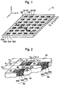
- Fig. 1 illustrates an anisotropic conductive sheet 10 according to an embodiment of the present invention.
- a Cartesian coordinate system XYZ of the anisotropic conductive sheet 10 is illustrated at a left upper part.
- the anisotropic conductive sheet 10 of this embodiment is a rectangular sheet member but may be a sheet member of a shape other than the rectangular shape.
- the anisotropic conductive sheet 10 has a constitution in which there are alternately arranged nonconductive strip-like members 12 and strip-like members 14 of a striped pattern having conductive pieces 24, 28 and nonconductive pieces 22, 26 that are alternately arranged.
- the nonconductive strip-like members 12 and the strip-like members 14 of the striped pattern adjoining each other are coupled by a coupling agent.
- the strip-like members 14 of the striped pattern are constituted by nonconductive pieces 22, 26, conductive pieces 24, 28, and conductive auxiliary layers 25, 29 in contact with the conductive pieces 24, 28.
- the members made of the nonconductive material constitute the nonconductive matrix, and the members made of the conductive material constitute conductive portions.
- the conductive portions are scattering, the scattering conductive portions are obtained. Therefore, the scattered conductive portions exist in the nonconductive matrix in a scattered manner.
- the conductive elastomer is a conductive silicone rubber manufactured by Shin-etsu Polymer Co.
- the nonconductive elastomer is a silicone rubber manufactured by Mitsubishi Jushi Co.
- the coupling agent is a silane coupling agent manufactured by Shin-etsu Polymer Co.
- a metal material is used as the conductive auxiliary layer, then, it may be called metal layer.
- Fig. 1 illustrates, on the left lower portion thereof, the anisotropic conductive sheet according to another embodiment with the broken surface as a boundary.
- the constitution of this embodiment is the same as that of the above embodiment except that the conductive auxiliary layers are adhered on both sides of the conductive pieces.
- conductive auxiliary layers 503 and 505 are adhered on both sides of the conductive piece 504 to improve the conductivity in the direction of thickness of the sheet.
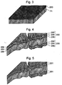
- Fig. 2 is a view illustrating on an enlarged scale the left upper corner portion of Fig. 1, i.e., illustrates the strip-like members 12 and 14 in further detail.
- the strip-like members 12 made of the nonconductive members of Fig. 1 correspond in Fig. 2 to strip-like members 20, 40, etc.
- the strip-like members 14 of the striped pattern of Fig. 1 the strip-like member including nonconductive pieces 22, 26, 30 ---, conductive pieces 24, 28 --- and conductive auxiliary layers 25, 29, --- corresponds to the strip-like member including nonconductive pieces 42, 46 ---, conductive pieces 44 --- and conductive auxiliary layers 45 ---.
- the nonconductive strip-like member 20 is neighbored by a strip-like member including nonconductive pieces 22, 26, ---, conductive pieces 24, 28, --- and conductive auxiliary layers 25, 29, --- which is further neighbored by a nonconductive strip-like member 40, and is further neighbored by a ship-like member including nonconductive pieces 42, 46. ---, conductive pieces 44, --- and conductive auxiliary layers 45, ---.
- the strip-like members have substantially the same thickness (T). The two strip-like members which are neighboring as described above are coupled together with the coupling agent.
- the conductive pieces with the conductive auxiliary layers and the nonconductive pieces that are neighboring to constitute the strip-like members 14 of the striped pattern, too, are coupled with the coupling agent to constitute a piece of sheet as shown in Fig. 1.
- the coupling agent is nonconductive, and the sheet maintains the non-conductivity in the direction of a plane.
- the conductive auxiliary layer 25 at the extreme left upper position is constituted by adhesive layers 242, 246 having thicknesses 1 t 21-1 and 1 t 21-3 and by a conductive layer 244 having a thickness 1 t 21-2 .
- other conductive auxiliary layers 29, 45 are constituted by adhesive layers 282, 286, conductive layer 284, adhesive layers 442, 446 and conductive layer 444.
- the adhesive layers are arranged on both sides of the conductive layer. In other embodiments, however, the adhesive layer may be arranged on either side only. It is, however, desired that the adhesive layer is between the conductive member and the conductive layer.
- the adhesive layer in this embodiment is constituted by the indium tin oxide, and the conductive layer is constituted by a copper alloy. In other embodiments, however, they may be replaced by other materials. These layers are formed by sputtering as will be described later.
- the nonconductive strip-like members 20, 40, --- have widths t 31 , t 32 , t 33 , ---, t 3k (k is a natural number), and the strip-like members 14 of the striped pattern have widths t 41 , ---, t 4k (k is a natural number).
- these widths are all the same. In other embodiments, however, the widths may be all the same or may be all different. These widths can be easily adjusted in the method of producing the anisotropic conductive sheet of the embodiment that will be described later.
- the strip-like members 14 of the striped pattern are constituted by nonconductive pieces 22, 28, 30, 34, ---, 42, 46, 50, 54, --- having lengths 1 t 11 , 1 t 12 , 1 t 13 , ---, 1 t 1m (m is a natural number); 2 t 11 , 2 t 12 , 2 t 13 , ---, 2 t 1n (n is a natural number), conductive pieces 24, 28, 32, ---, 44, 48, --- having lengths 1 t 21 , 1 t 22 , 1 t 23 , ---, 1 t 2m (m is a natural number); 2 t 21 , 2 t 22 , 2 t 23 , ---, 2 t 2n (n is a natural number), and conductive auxiliary layers 25, ---.
- the lengths of these nonconductive pieces and conductive pieces are all the same. In other embodiments, however, the lengths may all be the same or may be all different. These lengths can be easily adjusted in the method of producing the anisotropic conductive sheet of the embodiment that will be described later.
- the conductive pieces in the strip-like members of the striped pattern have a length of about 50 ⁇ m
- the nonconductive pieces have a length of about 30 ⁇ m
- the strip-like members of the striped pattern have a width of about 50 ⁇ m
- the nonconductive strip-like members have a width of about 50 ⁇ m.
- the lengths may be longer (or larger) or shorter (or smaller), as a matter of course.
- the extreme left upper conductive auxiliary layer 25 in this embodiment is constituted by the adhesive layer 242 in contact with the conductive piece 24, the conductive layer 244 in contact with the adhesive layer 242, and the adhesive layer 246 in contact with the conductive layer 244, the adhesive layer 246 being in contact with the nonconductive piece 26.
- the conductive auxiliary layers of this embodiment are formed by sputtering.
- the indium tin oxide is, first, deposited like a film, a copper alloy is deposited next like a film and, then, the indium tin oxide is deposited like a film.
- the boundaries of the layers are emphasized relatively clearly.
- the gradient of concentration may be mildly formed in the step of sputtering.
- the adhesive layer 242 has a thickness of about 500 angstroms
- the conductive layer 244 has a thickness of about 5000 angstroms
- the next adhesive layer 248 has a thickness of about 500 angstroms. Therefore, the conductive auxiliary layer has a thickness of about 6000 angstroms. In other embodiments, however, these thicknesses may be freely varied, as a matter of course. In the foregoing was described the extreme left upper conductive auxiliary layer 25 of the embodiment. However, the same also holds for other conductive auxiliary layers 25, 29, ---,
- the conductive auxiliary layer is thinner than the length (e.g., 1 t 21 ) of the conductive piece, more preferably, thinner than 1/10 thereof and, particularly preferably, thinner than 1/50 thereof.
- the length of the conductive piece is as great as 0.1 mm or more, it is desired that the conductive auxiliary layer has a thickness of not larger than 10 ⁇ m.
- the recurring distance is a value obtained by adding up the lengths of the two neighboring elastomers of different kinds, which is divided by 2, i.e., [( k t 1m + k t 2m )/2] or [( k t 1m + k t 2(m-1) )/2](k and m are natural numbers).
- the thickness of the adhesive layer has not been taken into consideration. This is because the thickness is usually very small as compared to their lengths (when great, it is desired that the thickness is also taken into consideration).
- an average value of these values may be used, a minimum value may be used, or a minimum value or an average value of a required place of the sheet may be used.
- the sheet as a whole exhibits fine pitch performance.
- the minimum value a minimum gap between the terminals that can be guaranteed is defined.
- the conductive elastomer is arranged relatively uniformly, further, the frequency of appearance of the conductive elastomer per a predetermined length may be used or the cumulative length of the conductive elastomer may be used in the strip-like members of the striped pattern.
- the recurring distance is about 40 ⁇ m even if an average value or a minimum value is used, and the cumulative length of the conductive elastomer per a unit length is about 0.6 mm/mm.
- the size of the anisotropic conductive sheet of this embodiment can be clearly indicated by adding up the widths and lengths described above. However, there is no limitation on the width or on the length and there is no limitation, either, on the thickness T. When used for connecting the circuit board to the terminals of the electronic parts, however, it is desired that the size matches with these sizes. In this case, the sizes are, usually, 0.5 to 3.0 cm x 0.5 to 3.0 cm and 0.5 to 2.0 mm in thickness.
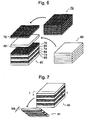
- Fig. 3 illustrates a conductive sheet 71 having a conductive auxiliary layer 250 adhered on the upper side thereof.
- the conductive auxiliary layer 250 can be adhered by various methods but is adhered by sputtering in this embodiment. Namely, the conductive sheet 71 is used as a base plate, a target is adjusted to meet the components of the conductive auxiliary layer to be prepared, and the conductive auxiliary layer is adhered by using a sputtering device.
- the conductive sheet of this embodiment is a conductive elastomer, and contrivance should be so made that the substrate temperature is not excessively elevated. For instance, there is used a magnetron or ion beam sputtering.
- Fig. 4 illustrates, on the left side thereof, the conductive sheet 71 with the conductive auxiliary layer 250 adhered on the upper side thereof partly being broken away.
- the conductive auxiliary layer is constituted by the adhesive layers 252, 256 and the conductive layer 254; i.e., the adhesive layer 256 is formed on the conductive sheet 71 and, then, the conductive layer 254 is formed and, finally, the adhesive layer 252 is formed.
- the conductive auxiliary layers are similarly adhered to both sides of the conductive sheet. This constitution enables the effect of the conductive auxiliary layers to be further exhibited.
- the above sheet member can be prepared by simultaneously adhering the conductive auxiliary layers onto both sides.
- one surface e.g., conductive auxiliary layer 250
- the conductive auxiliary layer 290 adhered onto the other surface is constituted by the adhesive layers 292, 296 and the conductive layer 294.
- the conductive auxiliary layer is to improve electric characteristics of the conductive sheet 71 and is, desirably, electrically contacted to the conductive sheet 71.
- the adhesive layers 256 and 292 are not to simply improve mechanical adhesion but also work to help electrical contact to the conductive layers 254 and 294.
- Fig. 5 is a view illustrating, partly in a cut-away manner, the conductive sheet 71 to which the conductive auxiliary layers 251 and 291 are adhered without adhesive layer.
- the left side of Fig. 5 is an embodiment in which the conductive auxiliary layer 251 is formed on the upper side only of the conductive sheet 71, and the right side is an embodiment in which the conductive auxiliary layers 251 and 291 are adhered to both sides of the conductive sheet 71.
- the structure is simpler than that of the case of Fig. 4, and the steps of manufacturing can be decreased.
- the conductive auxiliary layers 251 and 291 should be made of a material used for the conductive layers.
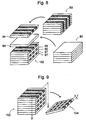
- conductive sheets (A) 70 with a conductive auxiliary layer and nonconductive sheets (B) 80 from which the sheet members are alternately stacked to prepare an AB sheet laminate (C) 90.
- AB sheet laminate (C) 90 On the AB sheet laminate (C) 90 being stacked, there are further stacked the nonconductive sheet (B) 82 and the conductive sheet (A) 72 with the conductive auxiliary layer further thereon. A coupling agent is applied among these sheet members so that the sheet members are coupled together.
- the nonconductive sheet (B) 83 is arranged at the lowest part of the AB sheet laminate (C) 90 which is being stacked. It should be noted that the thickness of this sheet member corresponds to 1 t 11 in Figs.
- the thickness of the conductive sheet (A) 73 just thereon corresponds to 1 t 21 in Fig. 2
- the thicknesses of the sheet members 84, 74, 85, 75 correspond, respectively, to the lengths of the conductive pieces 24, 28 and nonconductive pieces 22, 26 in Fig. 2. That is, lengths of the nonconductive piece and of the conductive piece with the conductive auxiliary layer in the strip-like member 14 of the striped pattern in Figs. 1 and 2 can be freely varied by varying the thickness of these sheet members.
- lengths of the conductive pieces and of the nonconductive pieces of the members of the strip-like member of the striped pattern sandwiched between the nonconductive strip-like members 40 correspond to the thickesses of the corresponding nonconductive sheet (B) and the conductive sheet (A).
- these thicknesses are not larger than about 80 ⁇ m and are, more, preferably, not larger than about 50 ⁇ m. In this embodiment, the thicknesses are so adjusted that the nonconductive pieces have a length of about 30 ⁇ m and the conductive pieces have a length of about 50 ⁇ m.
- the conductive sheets (A) may be continuously stacked in two or more pieces and, then, the nonconductive sheets (B) may be stacked in one or more pieces.
- the present invention may further include continuously stacking two or more pieces of nonconductive sheets (B) and, then, stacking one or more pieces of conductive sheets (A) alternately.
- Fig. 7 illustrates a first step of cutting the AB sheet laminate (C) 92 obtained by the step of obtaining the AB sheet laminate.
- the AB sheet laminate (C) 92 is cut along a cutting line 1-1 such that the thickness of the obtained zebra-like sheet 91 has a desired thickness t 4k (k is a natural number).
- This thickness t 4k corresponds to t 41 and t 42 in Fig 2.
- the widths of the strip-like members 14 of the striped pattern in Figs. 1 and 2 can be freely adjusted, and may all have the same width of different widths.
- the widths are not larger than about 80 ⁇ m and, more desirably, not larger than about 50 ⁇ m. In this embodiment, the widths are about 50 ⁇ m.
- Fig. 8 illustrates the preparation of the zebra-D sheet laminate (E) by alternately laminating the zebra-like sheet 93 prepared in the above step and the nonconductive sheet (D) 80.
- the nonconductive sheet (E) 100 On the zebra-D sheet laminate (E) 100 being stacked, there are further stacked the nonconductive sheet 84 and the zebra-like sheet 94 thereon. A coupling agent is applied among these sheet members so that the sheet members are coupled together.
- the nonconductive sheet (B) 87 is arranged at the lowest part of the zebra-D sheet laminate (E) 100 which is being stacked. It should be noted that the thickness of this sheet member corresponds to t 31 which is the width of the nonconductive strip-like member 12 in Fig.
- the thickness of the sheet member 97 just thereon corresponds to t 41 in Fig. 2
- the thicknesses of the sheet members 89, 99 correspond, respectively to t 32 . etc. in Fig. 2. That is, widths of the two kinds of strip-like members 12 and 14 in Figs. 1 and 2 can be freely varied by varying the thickness of these sheet members. Usually, as fine pitches, these thicknesses are not larger than about 80 ⁇ m and are, more, preferably, not larger than about 50 ⁇ m. In this embodiment, the thicknesses are so adjusted that the nonconductive strip-like members 12 have a width of about 30 ⁇ m and the strip-like members 14 of the striped pattern have a width of about 50 ⁇ m.
- Fig. 9 illustrates the step of cutting the zebra-D sheet laminate (E) 102 obtained through the step of obtaining the zebra-D sheet laminate.
- the laminate 102 is cut along a cutting line 2-2 such that the obtained anisotropic conductive sheet 104 will have a desired thickness T. Therefore, this makes it easy to prepare a thin anisotropic conductive sheet and a thick anisotropic conductive sheet which are usually difficult to obtain.
- the thickness is usually about 1 mm, the thickness can be decreased to be about 100 ⁇ m (or not larger than about 50 ⁇ m when particularly desired) or can be increased to be about several millimeters. In this embodiment, the thickness is selected to be about 1 mm.
- Figs. 10 and 11 are flowcharts illustrating a method of manufacturing the above anisotropic conductive sheet.
- Fig. 10 illustrates steps of preparing the zebra-like sheet.
- the conductive auxiliary layer is adhered on the conductive sheet (A)(S-01).
- the conductive auxiliary layer is formed by sputtering on one surface only of the conductive sheet.
- the conductive sheet (A) with the conductive auxiliary layer is stocked for use in the next step (S-02).
- the nonconductive sheet (B) is placed at a predetermined position for stacking (S-03).
- the coupling agent is applied onto the nonconductive sheet (B)(S-04).
- the conductive sheet (A) with the conductive auxiliary layer is placed thereon (S-05).
- the nonconductive sheet (B) is placed thereon (S-08).
- the routine proceeds to the first step of cutting (S-10). If the desired (predetermined) thickness has not been reached, the routine returns back to step S-04 where the coupling agent is optionally applied onto the conductive sheet (A).
- the zebra-like sheet is cut out piece by piece or in a plurality of number of pieces at one time, and the zebra-like sheets are stocked (S-11).
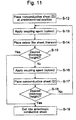
- Fig. 11 illustrates steps of preparing an anisotropic conductive sheet from the zebra-like sheet and the nonconductive sheet (D).
- the nonconductive sheet (D) is placed on a predetermined position for stacking (S-12).
- the coupling agent is applied onto the nonconductive sheet (D)(S-13).
- the zebra-like sheet is placed thereon (S-14).
- the nonconductive sheet (D) is placed thereon (S-17).
- the anisotropic sheet is cut out piece by piece or in a plurality of number of pieces at one time.
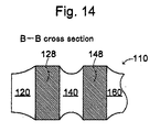
- Figs. 12, 13 and 14 illustrate another embodiment.
- an anisotropic conductive sheet 110 is prepared according to the above method by using conductive sheets that have been cured and nonconductive sheets that have not been cured.
- Figs. 13 and 14 are sectional views of the anisotropic conductive sheet 110 along the lines A-A and B-B.
- the conductive pieces 124, 128, 132 and 148 with the conductive auxiliary layer are protruded on the surface of the sheet to be higher than the nonconductive pieces 122, 128, 130, 134, 120, 140 and 160 offering improved reliability of contact. This form is assumed since uncured rubber has contracted due to the heating.
- the conductive elastomer has been cured and the nonconductive elastomer has not been cured.
- the uncured nonconductive elastomer can be adhered to the cured elastomer by heating or the like.
- the optional coupling agent needs not necessarily be added and may be omitted from the steps.
- the anisotropic conductive sheet of the present invention has the effect of not only maintaining insulation in the direction of the plane while exhibiting satisfactory conductivity in the direction of thickness but also enabling the sizes such as lengths of the nonconductive pieces and conductive pieces to be freely set to easily accomplish fine pitches desired for achieving a high degree of integration.
- the conductivity becomes particularly high.
- the conductive members and nonconductive members are chemically bonded together (crosslinking of rubber), the conductive portions do not slip out which, otherwise, tend to occur when a linear metal is used as conductive portions.
- the conductive pieces are necessarily surrounded by the nonconductive pieces avoiding contact caused by the approach/contact of conductive particles of a metal in the direction of plane of the anisotropic conductive sheet in which conductive particles are mixed.
Landscapes
- Engineering & Computer Science (AREA)
- Manufacturing & Machinery (AREA)
- Non-Insulated Conductors (AREA)
- Laminated Bodies (AREA)
Abstract
An anisotropic conductive sheet interposed between a circuit board
such as a substrate and various circuit parts to render them conductive and its
manufacturing method. The anisotropic conductive sheet has a fine pitch
required by the recent highly integrated circuit boards and electronic parts. In
the anisotropic conductive sheet in which conductive members are scattered in
a nonconductive matrix, the conductive members (e.g., 24) penetrate through
the sheet (10) in the direction of thickness and conductive auxiliary layers (e.g.,
25) are in contact with the conductive members (e.g., 24).
Description
This invention relates to an anisotropic conductive sheet which is
interposed between a circuit board such as a substrate and various circuit
components to conductive paths and to a manufacturing method thereof.
As electronic devices become smaller in size and thinner in thickness,
connecting minute circuits and connecting minute portions and circuitry are
more and more demanding. Connection methods thereof are based upon the
solder junction technology and the use of anisotropic conductive adhesive.
There is employed a method of interposing an anisotropic conductive
elastomer sheet between the electronic parts (components) and the circuit
board to render conductive paths.
The anisotropic conductive elastomer sheets include sheets having
conductivity only in the direction of thickness or conductivity only in the
direction of thickness when the sheets are compressed in the direction of
thickness. They have such features as accomplishing compact electric
connection without using such means as soldering or mechanical fitting, and
realizing a soft connection so as to absorb mechanical shocks and distortion.
Therefore, they have been extensively used as connectors for achieving
electric connection relative to circuit devices such as printed circuit board,
leadless chip carrier and liquid crystal panel in the fields of cell phones,
electronic calculators, electronic digital clocks, electronic cameras, computers
and the like.
In the electric test of the circuit devices such as printed circuit boards
and semiconductor integrated circuits, further, the anisotropic elastomer sheet
has heretofore been interposed between a region of electrodes of the circuit
device to be tested and a region of testing electrodes of the circuit board for
the test in order to achieve electric connection between the tested electrodes
formed on at least one surface of the circuit device to be tested and the testing
electrodes formed on the surface of the circuit board for the test.
It is known that an example of the above anisotropic conductive
elastomer sheet may be obtained by cutting an anisotropic conductive block in
a thin sheet such that the block that is formed integrally with thin metal wires
disposed in parallel and insulating material enclosing the metal wires is cut in a
direction orthogonal to the direction of the thin metal wires
(JP-A-2000-340037).
In the anisotropic conductive film with thin metal wires, however, it is
difficult to shorten distance between such thin metal wires and to secure
anisotropic conductivity with a fine pitch as required by recent highly integrated
circuit boards and electronic components. Further, it is likely that thin metal
wires are to be buckled with compressive force or the like during the use
thereof and easily pulled out after repetitive use so that the anisotropic
conductive film may fail to keep its function to a sufficient degree.
Therefore, this invention provides an anisotropic conductive sheet
having a fine pitch required by the recent highly integrated circuit boards and
electronic components, the anisotropic conductive sheet yet keeping high
conductivity in the direction of thickness and preventing conductive members
such as metals from slipping out.
In the present invention, it is provided an anisotropic conductive sheet
in which conductive members are scattered in a nonconductive matrix, wherein
the conductive members penetrate in the direction of thickness and conductive
auxiliary layers are in contact with the conductive members.
More specifically, the present invention provides the following.
In this invention, it is characterized in that an anisotropic conductive
sheet comprises conductive members scattered in the nonconductive matrix, in
which the conductive members penetrates the sheet in the thickness direction,
wherein the conductive auxiliary layers are in contact with the conductive
members. Here, the nonconductive matrix is a sheet member made of
nonconductive material so as to insulate the scattering conductive pieces in
directions contained in the plane of the sheet (directions in X-Y plane) to
maintain non-conductivity in the directions contained in the plane of the whole
anisotropic conductive sheet. Usually, the nonconductive matrix is all
connected (being continuous) in the anisotropic conductive sheet to form an
anisotropic conductive sheet. The nonconductive matrix, however, may not
have to be continuous. Further, the scattered conductive pieces may refer to
a condition that one or more conductive pieces made of a conductive material
are spread separately from each other in directions contained in the plane of
the sheet.
"The scattered conductive pieces made of a conductive material
penetrate the anisotropic conductive sheet from the front surface to the back
surface," may mean that the conductive pieces penetrate the sheet in the
thickness direction, may mean that the conductive pieces appear on both front
and back surfaces of the anisotropic conductive sheet, or may mean that the
sheet has a function for electrically connecting the front and back surfaces.
"The conductive auxiliary layers are in contact with the conductive members"
may mean that the conductive auxiliary layers are electrically connected to the
conductive members. The conductive auxiliary layers have conductivity
higher than the conductive members. When the electricity flows in parallel (as
being parallel-connected), therefore, the electric conductivity of the conductive
auxiliary layers become dominant in the entire conductivity. As a result, the
resistance between the front and the back of the sheet becomes low when the
conductive auxiliary layers are adhered, and may become equal to the
resistance of the conductive auxiliary layers. Here, the conductive auxiliary
layers that are made of metal material can be called metal layers. In the case
of the metal layer, the metal layer as a whole may be made of metal of a single
kind.
The anisotropic conductive sheet of the present invention expands on
a plane, and the feature of the sheet can be described by using X-direction and
Y-direction which are two directions in parallel with the plane, and Z-direction
orthogonal to X-direction and Y-direction. The anisotropic conductive sheet
has thickness in Z-direction, the strip-like member of the striped pattern has a
width in Y-direction and extends in X-direction, and the conductive pieces
made of conductive material and nonconductive pieces made of nonconductive
material are alternately arranged in X-direction. Further, the nonconductive
strip-like member has width in Y-direction and extends in X-direction. The
strip-like members having the striped pattern and the nonconductive strip-like
members are arranged in Y-direction, and are included in the anisotropic
conductive sheet in this state. In the strip-like members of the striped pattern,
the conductive auxiliary members are arranged among the conductive pieces
and the nonconductive pieces while in contact with the conductive pieces.
Being conductive may mean that the anisotropic conductive sheet of
such constitution has sufficiently high conductivity in the conduction direction.
It is usually preferable that the resistance among the terminals to be connected
is not larger than 100 Ω (preferably, not larger than 10 Ω and, more preferably
not larger than 1 Ω). The strip-like member of the striped pattern may be thin
and elongated in X-direction such that conductive members and nonconductive
members are alternately arranged along X-direction, wherein a striped pattern
may appear if the conductive members and the nonconductive members have
different colors. In practice, they need not appear in a striped pattern. The
alternate arrangement needs not expand over the whole strip-like members in
X-direction but may exist in only a portion thereof. Further, "the conductive
auxiliary layers being in contact with the conductive members" may stand for
the electric connection in the same manner as described above.
In the anisotropic conductive sheet of the present invention, further, it
may be characterized in that the conductive auxiliary layers comprise the
adhesive layers and the conductive layers. Here, the adhesive layers may be
those for improving the adhesion to the conductive members while the
conductive auxiliary layers come in contact with the conductive members.
The conductive layers of the conductive auxiliary layers have physical and
chemical properties which are greatly different from the physical and chemical
properties of the conductive members so that the adhesive layers have a
function to improve adhesion between them as the adhesive layers have
intermediate properties and bond the conductive layer and the conductive
member. Therefore, it may be characterized in that the adhesive layers are
arranged on the side of the conductive member being in contact with the
conductive auxiliary layers comprising the adhesive layers as a constituent
element. For example, it may be possible to lower or absorb distortion
caused by the different thermal expansion rate.
Further, it may be characterized in that the adhesive layer is arranged
on the side of the nonconductive matrix while the conductive auxiliary layer is
in contact with the nonconductive matrix. Here, being in contact with the
nonconductive matrix may mean that the conductive auxiliary layers are
physically (mechanically) in contact with the nonconductive matrix. This is
because the nonconductive matrix is insulative. Being arranged on the side
of the nonconductive matrix may mean that the adhesive layer is positioned
between the conductive layer and the nonconductive matrix. Here, the
adhesive layer may be a layer to improve the adhesion to the nonconductive
matrix while the conductive auxiliary layer is in contact with the nonconductive
matrix. The conductive layer of the conductive auxiliary layer has physical
and chemical properties which are greatly different from the physical and
chemical properties of the conductive member so that the adhesive layer can
have a function to improve the adhesion between them as the adhesive layer
has intermediate properties and bonds the conductive auxiliary layer and the
conductive member, Therefore, it may be characterized in that the adhesive
layers are arranged on the side of the conductive members which are in
contact with the conductive auxiliary layers comprising the adhesive layer as a
constituent element. For example, distortion caused by different thermal
expansion rate can be lowered or absorbed.
It may be characterized in that the adhesive layer comprises a metal
oxide or a metal. Examples of the metal oxide include indium oxide, tin oxide,
titanium oxide, a mixture thereof and a compound thereof, and examples of the
metal include chromium. For example, it may be characterized in that the
adhesive layer comprises indium tin oxide (or indium oxide / tin oxide).
Indium tin oxide (or indium oxide / tin oxide) is a ceramic material abbreviated
as ITO and has high electric conductivity. The conductive layer may be made
of metal having good conductivity. If the metal has electric conductivity higher
than that of the conductive members and if electricity flows in parallel therewith
(in a parallel-connected manner), the electric resistance of the metal controls
the entire electric resistance.
In the anisotropic conductive sheet of the present invention, further, it
may be characterized in that the nonconductive matrix comprises a
nonconductive elastomer, and the conductive members comprise a conductive
elastomer.
The conductive elastomer stands for an elastomer having electric
conductivity and is, usually, an elastomer blended with a conductive material
so as to lower the volume resistivity (smaller than, for example, 1 Ω-cm). For
examples, butadiene copolymers such as natural rubber, polyisoprene rubber,
butadiene/styrene, butadiene / acrylonitrile, butadiene / isobutylene,
conjugated diene rubber and hydrogenated compounds thereof; block
copolymer rubbers such as styrene/butadiene / diene block copolymer rubber,
styrene / isoprene block copolymer, and hydrogenated compounds thereof;
and chloroprene copolymer, vinyl chloride / vinyl acetate copolymer, urethane
rubber, polyester rubber, epichlorohydrin rubber, ethylene/propylene copolymer
rubber, ethylene / propylene/diene copolymer rubber, soft liquid epoxy rubber,
silicone rubber and fluorine-contained rubber may be utilized. Among them,
the silicone rubber is preferably used owing to its excellent heat resistance,
cold resistance, chemical resistance, aging resistance, electric insulation and
safety. The elastomer may be blended with a conductive substance like a
powder (flakes, small pieces, folls, etc. are allowable) of a metal such as gold,
silver, copper, nickel, tungsten, platinum, palladium or any other pure metal,
SUS, phosphor bronze or beryllium copper, or a nonmetallic powder (flakes,
small pieces, foils, etc. can be utilized) such as carbon powder to obtain a
conductive elastomer. Here, carbon may include carbon nano-tube and
fullerene.
The nonconductive elastomer stands for elastomer without conductivity
or having a very low conductivity, or elastomer having a sufficiently high
electric resistance. By way of example, butadiene copolymers such as
natural rubber, polyisoprene rubber, butadiene/styrene, butadiene / acrylonitrile,
butadiene / isobutylene, conjugated diene rubber and hydrogenated
compounds thereof; block copolymer rubbers such as styrene/butadiene /
diene block copolymer rubber, styrene / isoprene black copolymer, and
hydrogenated compounds thereof; and chloroprene copolymer, vinyl chloride /
vinyl acetate copolymer, urethane rubber, polyester rubber, epichlorohydrin
rubber, ethylene/propylene copolymer rubber, ethylene/propylene / diene
copolymer rubber, soft liquid epoxy rubber, silicone rubber and
fluorine-contained rubber may be employed. Among them, the silicone rubber
is preferably used owing to its excellent heat resistance, cold resistance,
chemical resistance, aging resistance, electric insulation and safety. The
nonconductive elastomer usually has high volume resistivity (e.g., not smaller
than 1 MΩ-cm at 100 V) and is nonconductive.
In order to chemically bond the conductive elastomer and the
nonconductive elastomer, a coupling agent may be applied between them.
The coupling agent is an agent for coupling these members, and may include
an adhesive commercially available. By way of example, coupling agents of
the types of silane, aluminum and titanate may be utilized. Among them, a
silane coupling agent is favorably used.
In the anisotropic conductive sheet of the present invention, it may be
characterized in that the conductive members are protruded as compared to
the nonconductive matrix. "Protruding" refers to a case where the portion of
the conductive member is thicker than the portion of the nonconductive matrix
in the thickness direction of the anisotropic sheet, a case where the position of
the upper surface of the nonconductive matrix is lower than the position of the
upper surface of the conductive member when the anisotropic conductive
sheet is horizontally placed, and/or a case where the position of the lower
surface of the nonconductive matrix is higher than the position of the lower
surface of the conductive member when the anisotropic conductive sheet is
horizontally placed. Then, the electric contact becomes more reliable to the
electronic parts and to the terminals of the substrate. This is because the
terminals, first, come in contact with the conductive members as they approach
the sheet such that a suitable degree of contact pressure is maintained due to
the pushing force to the sheet.
A method of manufacturing an anisotropic conductive sheet according
to the present invention comprises: a step of adhering conductive auxiliary
layers on the surface of a conductive sheet (A) made of conductive material to
obtain a conductive sheet (A) with the conductive auxiliary layers; a step of
alternately laminating the conductive sheet (A) with the conductive auxiliary
layers obtained in the step of adhering the layers and a nonconductive sheet
(B) to obtain an AB sheet laminate (C); a first step of cutting the AB sheet
laminate (C) obtained in the step of obtaining the AB sheet laminate to obtain a
zebra-like sheet in a predetermined thickness; a step of alternately laminating
the zebra-like sheet obtained in the first cutting step and a nonconductive
sheet (D) to obtain a zebra-D (ZD) sheet laminate (E); and a second step of
cutting the ZD sheet laminate (E) with a predetermined thickness obtained in
the step of obtaining the ZD sheet laminate.
Here, the conductive sheet (A) may be a sheet member of a single
kind or a collection of sheet members of different kinds. For example, the
conductive sheet (A) may be a collection of sheet members of the same
material but having different thicknesses. In the step of adhering the
conductive auxiliary layers onto the surface of the conductive sheet member
made of the conductive material, the conductive auxiliary layers may be
adhered onto one surface or both surfaces of the sheet members. The
conductive auxiliary layers can be adhered by any one of the vapor phase
method, liquid phase method or solid phase method or by a combination
thereof. Among them, the vapor phase is particularly preferred. As the
vapor phase method, there can be exemplified PVD such as sputtering method
and vacuum evaporation, and CVD. When the conductive auxiliary layer is
constituted by the adhesive layer and the conductive layer, the respective
layers may be adhered with the same method or with different methods.
The conductive sheet (A) with the conductive auxiliary layer and the
nonconductive sheet (B) may be the sheet members of a single kind as
described above or may be collections of sheet members of different kinds.
Alternate stacking may mean that the conductive sheet (A) with the conductive
auxiliary layer and the nonconductive sheet (B) are alternately stacked in any
order, which, however, does not exclude interposing a third sheet, a film or any
other members between the conductive sheet (A) with the conductive auxiliary
layer and the nonconductive sheet (B). In the step of stacking the sheet
members, further, a coupling agent may be applied among the sheets so that
the sheets are coupled together. The AB sheet laminate (C) prepared by
stacking may be heated in order to promote curing of the sheet members
themselves for increasing the coupling among the sheets or for any other
purposes.
The AB sheet laminate (C) can be cut with a blade such as a
cemented carbide cutter blade or a ceramic cutter blade, with a grindstone
such as a fine cutter, with a saw, or with any other cutting devices or cutting
instruments (which may include a cutting device of the non-contact type, such
as laser cutter). In the step of cutting, further, there may be used a cutting
fluid such as a cutting oil to prevent over-heating, to obtain finely cut surfaces
or for any other purpose, or a dry cutting may be employed. Further, the
object (e.g., work) to be cut may be cut alone or by being rotated together with
the cutting machine or instrument. It needs not be pointed out that a variety
of conditions for cutting are suitably selected to meet the AB sheet laminate (C).
To cut with a predetermined thickness may mean to cut the block to obtain a
sheet member having a predetermined thickness. The predetermined
thickness needs not be uniform but may vary depending upon the places of the
sheet member.
The step of obtaining the ZD sheet laminate (E) by alternately stacking
the zebra-like sheet and the nonconductive sheet (D) is the same as the step
of obtaining the AB sheet laminate (C) from the conductive sheet (A) and the
nonconductive sheet (B). Further, the second step of cutting the ZD sheet
laminate (E) in a predetermined thickness is the same as the first step of
cutting the AB sheet laminate (C).
The present invention will now be described in further detail by way of
embodiments with reference to the drawings. However, the embodiments are
simply to illustrate concrete materials and numerical values as preferred
examples of the present invention, but are not to limit the present invention.
Fig. 1 illustrates an anisotropic conductive sheet 10 according to an
embodiment of the present invention. A Cartesian coordinate system XYZ of
the anisotropic conductive sheet 10 is illustrated at a left upper part. The
anisotropic conductive sheet 10 of this embodiment is a rectangular sheet
member but may be a sheet member of a shape other than the rectangular
shape. The anisotropic conductive sheet 10 has a constitution in which there
are alternately arranged nonconductive strip-like members 12 and strip-like
members 14 of a striped pattern having conductive pieces 24, 28 and
nonconductive pieces 22, 26 that are alternately arranged. The
nonconductive strip-like members 12 and the strip-like members 14 of the
striped pattern adjoining each other are coupled by a coupling agent. The
strip-like members 14 of the striped pattern are constituted by nonconductive
pieces 22, 26, conductive pieces 24, 28, and conductive auxiliary layers 25, 29
in contact with the conductive pieces 24, 28. The members made of the
nonconductive material constitute the nonconductive matrix, and the members
made of the conductive material constitute conductive portions. When the
conductive portions are scattering, the scattering conductive portions are
obtained. Therefore, the scattered conductive portions exist in the
nonconductive matrix in a scattered manner. In the anisotropic conductive
sheet of this embodiment, the conductive elastomer is a conductive silicone
rubber manufactured by Shin-etsu Polymer Co., the nonconductive elastomer
is a silicone rubber manufactured by Mitsubishi Jushi Co. or a silicone rubber
manufactured by Shin-etsu Polymer Co., and the coupling agent is a silane
coupling agent manufactured by Shin-etsu Polymer Co. Here, if a metal
material is used as the conductive auxiliary layer, then, it may be called metal
layer.
Fig. 1 illustrates, on the left lower portion thereof, the anisotropic
conductive sheet according to another embodiment with the broken surface as
a boundary. The constitution of this embodiment is the same as that of the
above embodiment except that the conductive auxiliary layers are adhered on
both sides of the conductive pieces. For instance, conductive auxiliary layers
503 and 505 are adhered on both sides of the conductive piece 504 to improve
the conductivity in the direction of thickness of the sheet.
Fig. 2 is a view illustrating on an enlarged scale the left upper corner
portion of Fig. 1, i.e., illustrates the strip- like members 12 and 14 in further
detail. The strip-like members 12 made of the nonconductive members of Fig.
1 correspond in Fig. 2 to strip- like members 20, 40, etc. As for the strip-like
members 14 of the striped pattern of Fig. 1, the strip-like member including
nonconductive pieces 22, 26, 30 ---, conductive pieces 24, 28 --- and
conductive auxiliary layers 25, 29, --- corresponds to the strip-like member
including nonconductive pieces 42, 46 ---, conductive pieces 44 --- and
conductive auxiliary layers 45 ---. Namely, the nonconductive strip-like
member 20 is neighbored by a strip-like member including nonconductive
pieces 22, 26, ---, conductive pieces 24, 28, --- and conductive auxiliary layers
25, 29, --- which is further neighbored by a nonconductive strip-like member 40,
and is further neighbored by a ship-like member including nonconductive
pieces 42, 46. ---, conductive pieces 44, --- and conductive auxiliary layers 45,
---. In this embodiment, the strip-like members have substantially the same
thickness (T). The two strip-like members which are neighboring as
described above are coupled together with the coupling agent. The
conductive pieces with the conductive auxiliary layers and the nonconductive
pieces that are neighboring to constitute the strip-like members 14 of the
striped pattern, too, are coupled with the coupling agent to constitute a piece of
sheet as shown in Fig. 1. Here, the coupling agent is nonconductive, and the
sheet maintains the non-conductivity in the direction of a plane.
The conductive auxiliary layer 25 at the extreme left upper position is
constituted by adhesive layers 242, 246 having thicknesses 1t21-1 and 1t21-3 and
by a conductive layer 244 having a thickness 1t21-2. Similarly, other conductive
auxiliary layers 29, 45 are constituted by adhesive layers 282, 286, conductive
layer 284, adhesive layers 442, 446 and conductive layer 444. In this
embodiment, the adhesive layers are arranged on both sides of the conductive
layer. In other embodiments, however, the adhesive layer may be arranged
on either side only. It is, however, desired that the adhesive layer is between
the conductive member and the conductive layer. The adhesive layer in this
embodiment is constituted by the indium tin oxide, and the conductive layer is
constituted by a copper alloy. In other embodiments, however, they may be
replaced by other materials. These layers are formed by sputtering as will be
described later.
The nonconductive strip- like members 20, 40, --- have widths t31, t32,
t33, ---, t3k (k is a natural number), and the strip-like members 14 of the striped
pattern have widths t41, ---, t4k (k is a natural number). In this embodiment,
these widths are all the same. In other embodiments, however, the widths
may be all the same or may be all different. These widths can be easily
adjusted in the method of producing the anisotropic conductive sheet of the
embodiment that will be described later. Further, the strip-like members 14 of
the striped pattern are constituted by nonconductive pieces 22, 28, 30, 34, ---,
42, 46, 50, 54, --- having lengths 1t11, 1t12, 1t13, ---, 1t1m (m is a natural number);
2t11, 2t12, 2t13, ---, 2t1n (n is a natural number), conductive pieces 24, 28, 32, ---,
44, 48, --- having lengths 1t21, 1t22, 1t23, ---, 1t2m (m is a natural number); 2t21, 2t22,
2t23, ---, 2t2n (n is a natural number), and conductive auxiliary layers 25, ---. In
this embodiment, the lengths of these nonconductive pieces and conductive
pieces are all the same. In other embodiments, however, the lengths may all
be the same or may be all different. These lengths can be easily adjusted in
the method of producing the anisotropic conductive sheet of the embodiment
that will be described later. In this embodiment, the conductive pieces in the
strip-like members of the striped pattern have a length of about 50 µm, the
nonconductive pieces have a length of about 30 µm, the strip-like members of
the striped pattern have a width of about 50 µm and the nonconductive
strip-like members have a width of about 50 µm. In other embodiments,
however, the lengths may be longer (or larger) or shorter (or smaller), as a
matter of course.
The extreme left upper conductive auxiliary layer 25 in this
embodiment is constituted by the adhesive layer 242 in contact with the
conductive piece 24, the conductive layer 244 in contact with the adhesive
layer 242, and the adhesive layer 246 in contact with the conductive layer 244,
the adhesive layer 246 being in contact with the nonconductive piece 26. As
will be described later, the conductive auxiliary layers of this embodiment are
formed by sputtering. By using the conductive piece 24 as a base plate, the
indium tin oxide is, first, deposited like a film, a copper alloy is deposited next
like a film and, then, the indium tin oxide is deposited like a film. In this
embodiment, the boundaries of the layers are emphasized relatively clearly.
However, the gradient of concentration may be mildly formed in the step of
sputtering.
In this embodiment, the adhesive layer 242 has a thickness of about
500 angstroms, the conductive layer 244 has a thickness of about 5000
angstroms, and the next adhesive layer 248 has a thickness of about 500
angstroms. Therefore, the conductive auxiliary layer has a thickness of about
6000 angstroms. In other embodiments, however, these thicknesses may be
freely varied, as a matter of course. In the foregoing was described the
extreme left upper conductive auxiliary layer 25 of the embodiment. However,
the same also holds for other conductive auxiliary layers 25, 29, ---,
In general, it is desired that the conductive auxiliary layer is thinner
than the length (e.g., 1t21) of the conductive piece, more preferably, thinner than
1/10 thereof and, particularly preferably, thinner than 1/50 thereof. When the
length of the conductive piece is as great as 0.1 mm or more, it is desired that
the conductive auxiliary layer has a thickness of not larger than 10 µm.
In the case of this embodiment, the recurring distance is a value
obtained by adding up the lengths of the two neighboring elastomers of
different kinds, which is divided by 2, i.e., [(kt1m + kt2m)/2] or [(kt1m + kt2(m-1))/2](k
and m are natural numbers). Here, the thickness of the adhesive layer has
not been taken into consideration. This is because the thickness is usually
very small as compared to their lengths (when great, it is desired that the
thickness is also taken into consideration). As for the whole anisotropic
conductive sheet, an average value of these values may be used, a minimum
value may be used, or a minimum value or an average value of a required
place of the sheet may be used. When the average value is used, the sheet
as a whole exhibits fine pitch performance. When the minimum value is used,
a minimum gap between the terminals that can be guaranteed is defined.
When the conductive elastomer is arranged relatively uniformly, further, the
frequency of appearance of the conductive elastomer per a predetermined
length may be used or the cumulative length of the conductive elastomer may
be used in the strip-like members of the striped pattern. In this embodiment,
the recurring distance is about 40 µm even if an average value or a minimum
value is used, and the cumulative length of the conductive elastomer per a unit
length is about 0.6 mm/mm.
The size of the anisotropic conductive sheet of this embodiment can
be clearly indicated by adding up the widths and lengths described above.
However, there is no limitation on the width or on the length and there is no
limitation, either, on the thickness T. When used for connecting the circuit
board to the terminals of the electronic parts, however, it is desired that the
size matches with these sizes. In this case, the sizes are, usually, 0.5 to 3.0
cm x 0.5 to 3.0 cm and 0.5 to 2.0 mm in thickness.
A method of manufacturing the anisotropic conductive sheet of the
above embodiment will now be described with reference to Figs. 3 to 9. Fig. 3,
illustrates a conductive sheet 71 having a conductive auxiliary layer 250
adhered on the upper side thereof. The conductive auxiliary layer 250 can be
adhered by various methods but is adhered by sputtering in this embodiment.
Namely, the conductive sheet 71 is used as a base plate, a target is adjusted
to meet the components of the conductive auxiliary layer to be prepared, and
the conductive auxiliary layer is adhered by using a sputtering device. The
conductive sheet of this embodiment is a conductive elastomer, and
contrivance should be so made that the substrate temperature is not
excessively elevated. For instance, there is used a magnetron or ion beam
sputtering.
Fig. 4 illustrates, on the left side thereof, the conductive sheet 71 with
the conductive auxiliary layer 250 adhered on the upper side thereof partly
being broken away. In this embodiment, the conductive auxiliary layer is
constituted by the adhesive layers 252, 256 and the conductive layer 254; i.e.,
the adhesive layer 256 is formed on the conductive sheet 71 and, then, the
conductive layer 254 is formed and, finally, the adhesive layer 252 is formed.
On the right side of Fig. 4, the conductive auxiliary layers are similarly adhered
to both sides of the conductive sheet. This constitution enables the effect of
the conductive auxiliary layers to be further exhibited. The above sheet
member can be prepared by simultaneously adhering the conductive auxiliary
layers onto both sides. Usually, however, one surface (e.g., conductive
auxiliary layer 250) is, first, treated and is turned front side back, followed by
the adhesion of the conductive auxiliary layer 290 on the other surface. The
conductive auxiliary layer 290 adhered onto the other surface, too, is
constituted by the adhesive layers 292, 296 and the conductive layer 294.
The conductive auxiliary layer is to improve electric characteristics of the
conductive sheet 71 and is, desirably, electrically contacted to the conductive
sheet 71. The adhesive layers 256 and 292 are not to simply improve
mechanical adhesion but also work to help electrical contact to the conductive
layers 254 and 294.
Fig. 5 is a view illustrating, partly in a cut-away manner, the conductive
sheet 71 to which the conductive auxiliary layers 251 and 291 are adhered
without adhesive layer. The left side of Fig. 5 is an embodiment in which the
conductive auxiliary layer 251 is formed on the upper side only of the
conductive sheet 71, and the right side is an embodiment in which the
conductive auxiliary layers 251 and 291 are adhered to both sides of the
conductive sheet 71. In this embodiment, the structure is simpler than that of
the case of Fig. 4, and the steps of manufacturing can be decreased. The
conductive auxiliary layers 251 and 291 should be made of a material used for
the conductive layers.
Referring to Fig. 6, there are provided conductive sheets (A) 70 with a
conductive auxiliary layer and nonconductive sheets (B) 80, from which the
sheet members are alternately stacked to prepare an AB sheet laminate (C) 90.
On the AB sheet laminate (C) 90 being stacked, there are further stacked the
nonconductive sheet (B) 82 and the conductive sheet (A) 72 with the
conductive auxiliary layer further thereon. A coupling agent is applied among
these sheet members so that the sheet members are coupled together. The
nonconductive sheet (B) 83 is arranged at the lowest part of the AB sheet
laminate (C) 90 which is being stacked. It should be noted that the thickness
of this sheet member corresponds to 1t11 in Figs. 1 and 2, the thickness of the
conductive sheet (A) 73 just thereon corresponds to 1t21 in Fig. 2, and the
thicknesses of the sheet members 84, 74, 85, 75 correspond, respectively, to
the lengths of the conductive pieces 24, 28 and nonconductive pieces 22, 26 in
Fig. 2. That is, lengths of the nonconductive piece and of the conductive
piece with the conductive auxiliary layer in the strip-like member 14 of the
striped pattern in Figs. 1 and 2 can be freely varied by varying the thickness of
these sheet members. Similarly, lengths of the conductive pieces and of the
nonconductive pieces of the members of the strip-like member of the striped
pattern sandwiched between the nonconductive strip-like members 40,
correspond to the thickesses of the corresponding nonconductive sheet (B)
and the conductive sheet (A). Usually, as fine pitches, these thicknesses are
not larger than about 80 µm and are, more, preferably, not larger than about 50
µm. In this embodiment, the thicknesses are so adjusted that the
nonconductive pieces have a length of about 30 µm and the conductive pieces
have a length of about 50 µm.
To alternately stack the conductive sheets (A) and nonconductive
sheets (B), the conductive sheets (A) may be continuously stacked in two or
more pieces and, then, the nonconductive sheets (B) may be stacked in one or
more pieces. The present invention may further include continuously stacking
two or more pieces of nonconductive sheets (B) and, then, stacking one or
more pieces of conductive sheets (A) alternately.
Fig. 7 illustrates a first step of cutting the AB sheet laminate (C) 92
obtained by the step of obtaining the AB sheet laminate. The AB sheet
laminate (C) 92 is cut along a cutting line 1-1 such that the thickness of the
obtained zebra-like sheet 91 has a desired thickness t4k (k is a natural number).
This thickness t4k corresponds to t41 and t42 in Fig 2. Thus, the widths of the
strip-like members 14 of the striped pattern in Figs. 1 and 2 can be freely
adjusted, and may all have the same width of different widths. Usually, the
widths are not larger than about 80 µm and, more desirably, not larger than
about 50 µm. In this embodiment, the widths are about 50 µm.
Fig. 8 illustrates the preparation of the zebra-D sheet laminate (E) by
alternately laminating the zebra-like sheet 93 prepared in the above step and
the nonconductive sheet (D) 80. On the zebra-D sheet laminate (E) 100
being stacked, there are further stacked the nonconductive sheet 84 and the
zebra-like sheet 94 thereon. A coupling agent is applied among these sheet
members so that the sheet members are coupled together. The
nonconductive sheet (B) 87 is arranged at the lowest part of the zebra-D sheet
laminate (E) 100 which is being stacked. It should be noted that the thickness
of this sheet member corresponds to t31 which is the width of the
nonconductive strip-like member 12 in Fig. 2, the thickness of the sheet
member 97 just thereon corresponds to t41 in Fig. 2, and the thicknesses of the
sheet members 89, 99 correspond, respectively to t32. etc. in Fig. 2. That is,
widths of the two kinds of strip- like members 12 and 14 in Figs. 1 and 2 can be
freely varied by varying the thickness of these sheet members. Usually, as
fine pitches, these thicknesses are not larger than about 80 µm and are, more,
preferably, not larger than about 50 µm. In this embodiment, the thicknesses
are so adjusted that the nonconductive strip-like members 12 have a width of
about 30 µm and the strip-like members 14 of the striped pattern have a width
of about 50 µm.
Fig. 9 illustrates the step of cutting the zebra-D sheet laminate (E) 102
obtained through the step of obtaining the zebra-D sheet laminate. The
laminate 102 is cut along a cutting line 2-2 such that the obtained anisotropic
conductive sheet 104 will have a desired thickness T. Therefore, this makes it
easy to prepare a thin anisotropic conductive sheet and a thick anisotropic
conductive sheet which are usually difficult to obtain. Though the thickness is
usually about 1 mm, the thickness can be decreased to be about 100 µm (or
not larger than about 50 µm when particularly desired) or can be increased to
be about several millimeters. In this embodiment, the thickness is selected to
be about 1 mm.
Figs. 10 and 11 are flowcharts illustrating a method of manufacturing
the above anisotropic conductive sheet. Fig. 10 illustrates steps of preparing
the zebra-like sheet. First, the conductive auxiliary layer is adhered on the
conductive sheet (A)(S-01). In this embodiment, the conductive auxiliary
layer is formed by sputtering on one surface only of the conductive sheet.
The conductive sheet (A) with the conductive auxiliary layer is stocked for use
in the next step (S-02). Next, the nonconductive sheet (B) is placed at a
predetermined position for stacking (S-03). Optional, the coupling agent is
applied onto the nonconductive sheet (B)(S-04). This step may be omitted,
as a matter of course, since it is optional (the same holds hereinafter). The
conductive sheet (A) with the conductive auxiliary layer is placed thereon
(S-05). Check if the thickness (or height) of the stacked AB sheet laminate
(C) is reaching a desired thickness (or height)(S-06). If the desired
(predetermined) thickness has been reached, the routine proceeds to the first
step of cutting (S-10). If the desired (predetermined) thickness has not been
reached, the coupling agent is optionally applied onto the conductive sheet
(A)(S-07). The nonconductive sheet (B) is placed thereon (S-08). Check if
the thickness (or height) of the stacked AB sheet laminate (C) is reaching a
desired thickness (or height)(S-09). If the desired (predetermined) thickness
has been reached, the routine proceeds to the first step of cutting (S-10). If
the desired (predetermined) thickness has not been reached, the routine
returns back to step S-04 where the coupling agent is optionally applied onto
the conductive sheet (A). At the step of cutting (S-10), the zebra-like sheet is
cut out piece by piece or in a plurality of number of pieces at one time, and the
zebra-like sheets are stocked (S-11).
Fig. 11 illustrates steps of preparing an anisotropic conductive sheet
from the zebra-like sheet and the nonconductive sheet (D). First, the
nonconductive sheet (D) is placed on a predetermined position for stacking
(S-12). Optionally, the coupling agent is applied onto the nonconductive sheet
(D)(S-13). The zebra-like sheet is placed thereon (S-14). Check if the
thickness (or height) of the stacked zebra-D sheet laminate (E) is reaching a
desired thickness (or height)(S-15). If the desired (predetermined) thickness
has been reached, the routine proceeds to the second step of cutting (S-19).
If the desired (predetermined) thickness has not been reached, the coupling
agent is optionally applied onto the zebra-like sheet (S-16). The
nonconductive sheet (D)is placed thereon (S-17). Check if the thickness (or
height) of the zebra-D sheet laminate (E) is reaching a desired thickness (or
height)(S-18). If the desired (predetermined) thickness has been reached, the
routine proceeds to the second step of cutting (S-19). If the desired
(predetermined) thickness has not been reached, the routine returns back to
step S-13 where the coupling agent is optionally applied onto the
nonconductive sheet (D). At the second step of cutting (S-19), the anisotropic
sheet is cut out piece by piece or in a plurality of number of pieces at one time.
Figs. 12, 13 and 14 illustrate another embodiment. In this
embodiment, an anisotropic conductive sheet 110 is prepared according to the
above method by using conductive sheets that have been cured and
nonconductive sheets that have not been cured. Figs. 13 and 14 are
sectional views of the anisotropic conductive sheet 110 along the lines A-A and
B-B. As will be understood from these drawings, the conductive pieces 124,
128, 132 and 148 with the conductive auxiliary layer are protruded on the
surface of the sheet to be higher than the nonconductive pieces 122, 128, 130,
134, 120, 140 and 160 offering improved reliability of contact. This form is
assumed since uncured rubber has contracted due to the heating. Here, the
conductive elastomer has been cured and the nonconductive elastomer has
not been cured. The uncured nonconductive elastomer can be adhered to the
cured elastomer by heating or the like. In the above manufacturing method,
therefore, the optional coupling agent needs not necessarily be added and
may be omitted from the steps.
As described above, the anisotropic conductive sheet of the present
invention has the effect of not only maintaining insulation in the direction of the
plane while exhibiting satisfactory conductivity in the direction of thickness but
also enabling the sizes such as lengths of the nonconductive pieces and
conductive pieces to be freely set to easily accomplish fine pitches desired for
achieving a high degree of integration. When the conductive auxiliary layer
penetrating through in the direction of thickness is directly exposed on the front
surface and on the back surface, it is considered that the conductivity becomes
particularly high. Further, since the conductive members and nonconductive
members are chemically bonded together (crosslinking of rubber), the
conductive portions do not slip out which, otherwise, tend to occur when a
linear metal is used as conductive portions. Besides, the conductive pieces
are necessarily surrounded by the nonconductive pieces avoiding contact
caused by the approach/contact of conductive particles of a metal in the
direction of plane of the anisotropic conductive sheet in which conductive
particles are mixed.
Claims (11)
- An anisotropic conductive sheet expanding on a first plane, wherein: when a first direction contained in said first plane is denoted as X-direction, a direction orthogonal to X-direction and contained in said first plane is denoted as Y-direction and a direction orthogonal to X-direction and Y-direction is denoted as Z-direction; and the anisotropic conductive sheet has a predetermined thickness in Z-direction and a front surface and a back surface substantially in parallel with said first plane, the anisotropic conductive sheet comprising: a nonconductive matrix expanding on said first plane; conductive pieces scattered in the nonconductive matrix; and conductive auxiliary layers in contact with the scattered conductive pieces, wherein said scattered conductive pieces extend in Z-direction so as to penetrate the anisotropic conductive sheet from the front surface to the back surface.
- The anisotropic conductive sheet according to claim 1, wherein said conductive auxiliary layers penetrate the anisotropic conductive sheet from the front surface to the back surface along the scattered conductive pieces.
- An anisotropic conductive sheet expanding on a first plane, wherein: when a first direction contained in said first plane is denoted as X-direction, a direction orthogonal to X-direction and contained in said first plane is denoted as Y-direction and a direction orthogonal to X-direction and Y-direction is denoted as Z-direction, and the anisotropic conductive sheet has a predetermined thickness in Z-direction and a front surface and a back surface substantial in parallel with said first plane, the anisotropic conductive sheet comprising: strip-like members of a striped pattern having a width in Y-direction and extending in X-direction and conductive pieces and nonconductive pieces alternately arranged in X-direction; and nonconductive strip-like members having a width in Y-direction and extending in X-direction, wherein the strip-like members and the nonconductive strip-like members are arranged relative to each other in Y-direction, and wherein in said strip-like members of a striped pattern, a conductive auxiliary layer is arranged between the conductive piece and the nonconductive piece while in contact with said conductive piece.
- The anisotropic conductive sheet according to any one of claims 1 to 3, wherein the conductive auxiliary layer comprises an adhesive layer and a conductive layer.
- The anisotropic conductive sheet according to any one of claims 1 to 4, wherein the adhesive layer is arranged on a conductive piece side of the conductive auxiliary layer.
- The anisotropic conductive sheet according to claim 4 or 5, wherein the adhesive layer comprises indium tin oxide.
- The anisotropic conductive sheet according to any one of clalms 4 to 6, wherein the conductive layer is made of material having good conductivity.
- The anisotropic conductive sheet according to claim 1 or 2, wherein the nonconductive matrix comprises a conductive elastomer and the scattering conductive pieces comprise a conductive elastomer.
- The anisotropic conductive sheet according to claim 3, wherein the nonconductive pieces and the nonconductive strip-like members comprise a nonconductive elastomer and the conductive pieces comprise a conductive elastomer.
- The anisotropic conductive sheet according to any one of claims 1 to 9, wherein the scattered conductive pieces or the conductive pieces are protruded as compared to surroundings thereof along Z-direction.
- A method of manufacturing a flexible anisotropic conductive sheet having a predetermined thickness, and predetermined front and back surfaces on the front and back across the thickness, the method comprising: a step of adhering a conductive auxiliary layer on the surface of a conductive sheet (A) made of a conductive member so as to obtain a conductive sheet (A) with the conductive auxiliary layer; a step of alternately laminating the conductive sheet (A) with the conductive auxiliary layer obtained in the step of adhering the layers and a nonconductive sheet (B) so as to obtain an AB sheet laminate (C); a first step of cutting the AB sheet laminate (C) obtained in the step of obtaining the AB sheet laminate to obtain a zebra-like sheet in a predetermined thickness; a step of alternately laminating the zebra-like sheet obtained in the first cutting step and a nonconductive sheet (D) to obtain a ZD sheet laminate (E); and a second step of cutting the ZD sheet laminate (E) with a predetermined thickness, which is obtained in the step of obtaining the ZD sheet laminate.
Applications Claiming Priority (3)
| Application Number | Priority Date | Filing Date | Title |
|---|---|---|---|
| JP2002079748 | 2002-03-20 | ||
| JP2002079748 | 2002-03-20 | ||
| PCT/JP2003/003462 WO2003079496A1 (en) | 2002-03-20 | 2003-03-20 | Anisotropic conductive sheet and its manufacturing method |
Publications (2)
| Publication Number | Publication Date |
|---|---|
| EP1487057A1 true EP1487057A1 (en) | 2004-12-15 |
| EP1487057A4 EP1487057A4 (en) | 2006-08-16 |
Family
ID=28035674
Family Applications (1)
| Application Number | Title | Priority Date | Filing Date |
|---|---|---|---|
| EP03744535A Withdrawn EP1487057A4 (en) | 2002-03-20 | 2003-03-20 | CONDUCTIVE ANISOTROPIC SHEET AND PROCESS FOR PRODUCING THE SAME |
Country Status (8)
| Country | Link |
|---|---|
| US (1) | US7465491B2 (en) |
| EP (1) | EP1487057A4 (en) |
| JP (1) | JPWO2003079496A1 (en) |
| KR (1) | KR20050005421A (en) |
| CN (1) | CN100477387C (en) |
| AU (1) | AU2003220943A1 (en) |
| TW (1) | TWI244657B (en) |
| WO (1) | WO2003079496A1 (en) |
Cited By (1)
| Publication number | Priority date | Publication date | Assignee | Title |
|---|---|---|---|---|
| EP2947685A4 (en) * | 2013-11-22 | 2016-04-27 | Silicone Valley Co Ltd | SEMICONDUCTOR TEST RANGE HAVING STACKED METALLIC SHEETS AND METHOD FOR MANUFACTURING THE SAME |
Families Citing this family (7)
| Publication number | Priority date | Publication date | Assignee | Title |
|---|---|---|---|---|
| US8518304B1 (en) | 2003-03-31 | 2013-08-27 | The Research Foundation Of State University Of New York | Nano-structure enhancements for anisotropic conductive material and thermal interposers |
| US20090115004A1 (en) * | 2003-12-30 | 2009-05-07 | 3M Innovative Properties Company | Surface acoustic wave sensor assemblies |
| JP2005251654A (en) * | 2004-03-05 | 2005-09-15 | Jst Mfg Co Ltd | Anisotropic conductive sheet and manufacturing method thereof |
| JP2005259475A (en) * | 2004-03-10 | 2005-09-22 | Jst Mfg Co Ltd | Anisotropic conductive sheet |
| JP2008023768A (en) * | 2006-07-19 | 2008-02-07 | Brother Ind Ltd | Head unit thickness management method and manufacturing method |
| KR101435459B1 (en) * | 2014-03-26 | 2014-08-28 | 실리콘밸리(주) | Semiconductor test pad using adhesive and stacked thin sheets of metal and manufacturing method thereof |
| JP6422676B2 (en) * | 2014-06-04 | 2018-11-14 | 日東電工株式会社 | Transparent conductive film |
Family Cites Families (23)
| Publication number | Priority date | Publication date | Assignee | Title |
|---|---|---|---|---|
| JPS5187787A (en) | 1975-01-31 | 1976-07-31 | Shinetsu Polymer Co | Intaa konekutaa |
| US3982320A (en) | 1975-02-05 | 1976-09-28 | Technical Wire Products, Inc. | Method of making electrically conductive connector |
| JPS57138791A (en) | 1981-02-20 | 1982-08-27 | Shinetsu Polymer Co | Method of producing anisotropic conductive connector |
| JPS57141807A (en) | 1981-02-25 | 1982-09-02 | Shinetsu Polymer Co | Method of producing low pitch connector |
| JPS6050468U (en) | 1983-09-14 | 1985-04-09 | 株式会社日立製作所 | Anisotropic conductive rubber connector |
| JPS60264071A (en) | 1984-06-13 | 1985-12-27 | 住友ベークライト株式会社 | Method of producing connector part |
| JPS63117066U (en) | 1987-01-23 | 1988-07-28 | ||
| JPH04341774A (en) | 1991-05-16 | 1992-11-27 | Shin Etsu Polymer Co Ltd | Low-resistance pressure-contact type connector |
| JPH0685334B2 (en) * | 1992-05-29 | 1994-10-26 | 第二しなのポリマー株式会社 | Anisotropic conductive connector |
| JPH0661600A (en) * | 1992-08-07 | 1994-03-04 | Mitsui Toatsu Chem Inc | Flexible circuit board |
| JP2722957B2 (en) | 1992-08-11 | 1998-03-09 | 株式会社村田製作所 | Modular connector |
| JPH07153313A (en) * | 1993-12-01 | 1995-06-16 | Sumitomo Metal Mining Co Ltd | Translucent conductive adhesive |
| JP3670338B2 (en) | 1995-04-19 | 2005-07-13 | Jsr株式会社 | Circuit board inspection adapter device |
| JPH0997643A (en) * | 1995-09-29 | 1997-04-08 | Shin Etsu Polymer Co Ltd | Low resistance connector and manufacture thereof |
| JPH11231010A (en) | 1998-02-12 | 1999-08-27 | Jsr Corp | Multi-layer connector and adapter device for circuit board inspection |
| JPH11260446A (en) | 1998-03-11 | 1999-09-24 | Jsr Corp | Multilayer connector and adapter device for circuit device inspection |
| JPH11345643A (en) | 1998-06-01 | 1999-12-14 | Jsr Corp | Multilayer connector, adapter and adapter device for circuit device inspection |
| JP2000058158A (en) | 1998-08-05 | 2000-02-25 | Jsr Corp | Connector, method of manufacturing the same, and adapter device for circuit device inspection |
| JP2000113923A (en) | 1998-10-08 | 2000-04-21 | Jsr Corp | Adapter device and circuit board inspection device |
| JP2000243489A (en) | 1999-02-23 | 2000-09-08 | Jsr Corp | Wiring board forming material, plate-like connector, method of manufacturing the same, and adapter device for circuit device inspection |
| JP2000340037A (en) | 1999-05-31 | 2000-12-08 | Taiyo Yuden Co Ltd | Anisotropic conductive membrane and its manufacture |
| JP2001266975A (en) | 2000-03-23 | 2001-09-28 | Fuji Kobunshi Kogyo Kk | Heat welding anisotropic conductive elastic connector and its manufacturing method |
| JP4255200B2 (en) | 2000-05-19 | 2009-04-15 | 信越ポリマー株式会社 | Low resistance connector |
-
2003
- 2003-03-20 CN CNB038065681A patent/CN100477387C/en not_active Expired - Fee Related
- 2003-03-20 KR KR10-2004-7014598A patent/KR20050005421A/en not_active Withdrawn
- 2003-03-20 WO PCT/JP2003/003462 patent/WO2003079496A1/en not_active Ceased
- 2003-03-20 AU AU2003220943A patent/AU2003220943A1/en not_active Abandoned
- 2003-03-20 TW TW092106159A patent/TWI244657B/en not_active IP Right Cessation
- 2003-03-20 US US10/508,049 patent/US7465491B2/en not_active Expired - Fee Related
- 2003-03-20 JP JP2003577381A patent/JPWO2003079496A1/en active Pending
- 2003-03-20 EP EP03744535A patent/EP1487057A4/en not_active Withdrawn
Cited By (1)
| Publication number | Priority date | Publication date | Assignee | Title |
|---|---|---|---|---|
| EP2947685A4 (en) * | 2013-11-22 | 2016-04-27 | Silicone Valley Co Ltd | SEMICONDUCTOR TEST RANGE HAVING STACKED METALLIC SHEETS AND METHOD FOR MANUFACTURING THE SAME |
Also Published As
| Publication number | Publication date |
|---|---|
| CN100477387C (en) | 2009-04-08 |
| EP1487057A4 (en) | 2006-08-16 |
| TW200402071A (en) | 2004-02-01 |
| US7465491B2 (en) | 2008-12-16 |
| US20050145974A1 (en) | 2005-07-07 |
| KR20050005421A (en) | 2005-01-13 |
| AU2003220943A1 (en) | 2003-09-29 |
| CN1643740A (en) | 2005-07-20 |
| JPWO2003079496A1 (en) | 2005-07-21 |
| TWI244657B (en) | 2005-12-01 |
| WO2003079496A1 (en) | 2003-09-25 |
Similar Documents
| Publication | Publication Date | Title |
|---|---|---|
| US20050224762A1 (en) | Flexible good conductive layer and anisotropic conductive sheet comprising same | |
| US7244127B2 (en) | Anisotropic conductive sheet and its manufacturing method | |
| US7465491B2 (en) | Anisotropic conductive sheet and its manufacturing method | |
| EP1487055A1 (en) | Anisotropic conductive sheet and its manufacturing method | |
| JP4236367B2 (en) | Semiconductor socket and manufacturing method thereof | |
| US7304390B2 (en) | Anisotropic conductive sheet and manufacture thereof | |
| US20090078449A1 (en) | Dielectric sheet | |
| US7264482B2 (en) | Anisotropic conductive sheet | |
| CN100505424C (en) | Anisotropic conductive block and method for manufacturing the same | |
| US7419387B2 (en) | Electric connection member utilizing ansiotropically conductive sheets |
Legal Events
| Date | Code | Title | Description |
|---|---|---|---|
| PUAI | Public reference made under article 153(3) epc to a published international application that has entered the european phase |
Free format text: ORIGINAL CODE: 0009012 |
|
| 17P | Request for examination filed |
Effective date: 20040916 |
|
| AK | Designated contracting states |
Kind code of ref document: A1 Designated state(s): AT BE BG CH CY CZ DE DK EE ES FI FR GB GR HU IE IT LI LU MC NL PT RO SE SI SK TR |
|
| AX | Request for extension of the european patent |
Extension state: AL LT LV MK |
|
| A4 | Supplementary search report drawn up and despatched |
Effective date: 20060717 |
|
| STAA | Information on the status of an ep patent application or granted ep patent |
Free format text: STATUS: THE APPLICATION IS DEEMED TO BE WITHDRAWN |
|
| 18D | Application deemed to be withdrawn |
Effective date: 20061021 |