EP1487008A2 - Verfahren zur Herstellung eines Siliziumfilms, ein Siliziumfilm und eine Solarbatterie - Google Patents
Verfahren zur Herstellung eines Siliziumfilms, ein Siliziumfilm und eine Solarbatterie Download PDFInfo
- Publication number
- EP1487008A2 EP1487008A2 EP04013647A EP04013647A EP1487008A2 EP 1487008 A2 EP1487008 A2 EP 1487008A2 EP 04013647 A EP04013647 A EP 04013647A EP 04013647 A EP04013647 A EP 04013647A EP 1487008 A2 EP1487008 A2 EP 1487008A2
- Authority
- EP
- European Patent Office
- Prior art keywords
- melt
- substrate
- temperature
- melting point
- thin film
- Prior art date
- Legal status (The legal status is an assumption and is not a legal conclusion. Google has not performed a legal analysis and makes no representation as to the accuracy of the status listed.)
- Withdrawn
Links
Images


Classifications
-
- H—ELECTRICITY
- H10—SEMICONDUCTOR DEVICES; ELECTRIC SOLID-STATE DEVICES NOT OTHERWISE PROVIDED FOR
- H10F—INORGANIC SEMICONDUCTOR DEVICES SENSITIVE TO INFRARED RADIATION, LIGHT, ELECTROMAGNETIC RADIATION OF SHORTER WAVELENGTH OR CORPUSCULAR RADIATION
- H10F71/00—Manufacture or treatment of devices covered by this subclass
- H10F71/121—The active layers comprising only Group IV materials
-
- C—CHEMISTRY; METALLURGY
- C30—CRYSTAL GROWTH
- C30B—SINGLE-CRYSTAL GROWTH; UNIDIRECTIONAL SOLIDIFICATION OF EUTECTIC MATERIAL OR UNIDIRECTIONAL DEMIXING OF EUTECTOID MATERIAL; REFINING BY ZONE-MELTING OF MATERIAL; PRODUCTION OF A HOMOGENEOUS POLYCRYSTALLINE MATERIAL WITH DEFINED STRUCTURE; SINGLE CRYSTALS OR HOMOGENEOUS POLYCRYSTALLINE MATERIAL WITH DEFINED STRUCTURE; AFTER-TREATMENT OF SINGLE CRYSTALS OR A HOMOGENEOUS POLYCRYSTALLINE MATERIAL WITH DEFINED STRUCTURE; APPARATUS THEREFOR
- C30B19/00—Liquid-phase epitaxial-layer growth
-
- C—CHEMISTRY; METALLURGY
- C30—CRYSTAL GROWTH
- C30B—SINGLE-CRYSTAL GROWTH; UNIDIRECTIONAL SOLIDIFICATION OF EUTECTIC MATERIAL OR UNIDIRECTIONAL DEMIXING OF EUTECTOID MATERIAL; REFINING BY ZONE-MELTING OF MATERIAL; PRODUCTION OF A HOMOGENEOUS POLYCRYSTALLINE MATERIAL WITH DEFINED STRUCTURE; SINGLE CRYSTALS OR HOMOGENEOUS POLYCRYSTALLINE MATERIAL WITH DEFINED STRUCTURE; AFTER-TREATMENT OF SINGLE CRYSTALS OR A HOMOGENEOUS POLYCRYSTALLINE MATERIAL WITH DEFINED STRUCTURE; APPARATUS THEREFOR
- C30B29/00—Single crystals or homogeneous polycrystalline material with defined structure characterised by the material or by their shape
- C30B29/02—Elements
- C30B29/06—Silicon
-
- H—ELECTRICITY
- H10—SEMICONDUCTOR DEVICES; ELECTRIC SOLID-STATE DEVICES NOT OTHERWISE PROVIDED FOR
- H10P—GENERIC PROCESSES OR APPARATUS FOR THE MANUFACTURE OR TREATMENT OF DEVICES COVERED BY CLASS H10
- H10P14/00—Formation of materials, e.g. in the shape of layers or pillars
- H10P14/20—Formation of materials, e.g. in the shape of layers or pillars of semiconductor materials
- H10P14/26—Formation of materials, e.g. in the shape of layers or pillars of semiconductor materials using liquid deposition
- H10P14/263—Formation of materials, e.g. in the shape of layers or pillars of semiconductor materials using liquid deposition using melted materials
-
- H—ELECTRICITY
- H10—SEMICONDUCTOR DEVICES; ELECTRIC SOLID-STATE DEVICES NOT OTHERWISE PROVIDED FOR
- H10P—GENERIC PROCESSES OR APPARATUS FOR THE MANUFACTURE OR TREATMENT OF DEVICES COVERED BY CLASS H10
- H10P14/00—Formation of materials, e.g. in the shape of layers or pillars
- H10P14/20—Formation of materials, e.g. in the shape of layers or pillars of semiconductor materials
- H10P14/29—Formation of materials, e.g. in the shape of layers or pillars of semiconductor materials characterised by the substrates
- H10P14/2901—Materials
- H10P14/2902—Materials being Group IVA materials
- H10P14/2905—Silicon, silicon germanium or germanium
-
- H—ELECTRICITY
- H10—SEMICONDUCTOR DEVICES; ELECTRIC SOLID-STATE DEVICES NOT OTHERWISE PROVIDED FOR
- H10P—GENERIC PROCESSES OR APPARATUS FOR THE MANUFACTURE OR TREATMENT OF DEVICES COVERED BY CLASS H10
- H10P14/00—Formation of materials, e.g. in the shape of layers or pillars
- H10P14/20—Formation of materials, e.g. in the shape of layers or pillars of semiconductor materials
- H10P14/34—Deposited materials, e.g. layers
- H10P14/3402—Deposited materials, e.g. layers characterised by the chemical composition
- H10P14/3404—Deposited materials, e.g. layers characterised by the chemical composition being Group IVA materials
- H10P14/3411—Silicon, silicon germanium or germanium
-
- H—ELECTRICITY
- H10—SEMICONDUCTOR DEVICES; ELECTRIC SOLID-STATE DEVICES NOT OTHERWISE PROVIDED FOR
- H10P—GENERIC PROCESSES OR APPARATUS FOR THE MANUFACTURE OR TREATMENT OF DEVICES COVERED BY CLASS H10
- H10P14/00—Formation of materials, e.g. in the shape of layers or pillars
- H10P14/20—Formation of materials, e.g. in the shape of layers or pillars of semiconductor materials
- H10P14/34—Deposited materials, e.g. layers
- H10P14/3438—Doping during depositing
- H10P14/3441—Conductivity type
-
- Y—GENERAL TAGGING OF NEW TECHNOLOGICAL DEVELOPMENTS; GENERAL TAGGING OF CROSS-SECTIONAL TECHNOLOGIES SPANNING OVER SEVERAL SECTIONS OF THE IPC; TECHNICAL SUBJECTS COVERED BY FORMER USPC CROSS-REFERENCE ART COLLECTIONS [XRACs] AND DIGESTS
- Y02—TECHNOLOGIES OR APPLICATIONS FOR MITIGATION OR ADAPTATION AGAINST CLIMATE CHANGE
- Y02E—REDUCTION OF GREENHOUSE GAS [GHG] EMISSIONS, RELATED TO ENERGY GENERATION, TRANSMISSION OR DISTRIBUTION
- Y02E10/00—Energy generation through renewable energy sources
- Y02E10/50—Photovoltaic [PV] energy
- Y02E10/547—Monocrystalline silicon PV cells
-
- Y—GENERAL TAGGING OF NEW TECHNOLOGICAL DEVELOPMENTS; GENERAL TAGGING OF CROSS-SECTIONAL TECHNOLOGIES SPANNING OVER SEVERAL SECTIONS OF THE IPC; TECHNICAL SUBJECTS COVERED BY FORMER USPC CROSS-REFERENCE ART COLLECTIONS [XRACs] AND DIGESTS
- Y02—TECHNOLOGIES OR APPLICATIONS FOR MITIGATION OR ADAPTATION AGAINST CLIMATE CHANGE
- Y02P—CLIMATE CHANGE MITIGATION TECHNOLOGIES IN THE PRODUCTION OR PROCESSING OF GOODS
- Y02P70/00—Climate change mitigation technologies in the production process for final industrial or consumer products
- Y02P70/50—Manufacturing or production processes characterised by the final manufactured product
Definitions
- This invention relates to a method for forming a Si film, the same Si film, and a solar battery which is made of the same Si film by means of the same forming method.
- the casting method since the casting method, however, utilizes a solidifying method of melt where the temperature gradient of the solid-liquid interface is increased, it is inherently difficult to develop the crystal quality of the obtained Si polycrystal. Moreover, since pure Si raw materials are expensive, the quality of Si raw materials to be employed is restricted. In this point of view, such a thin film growing method as to form a Si film on an inorganic substrate by means of vapor phase epitaxy has been also developed, in addition to the above-mentioned manufacturing technology.
- the thin film growing method since epitaxial growing technique utilizing a crystal substrate is not employed, but driving force of growth obtained on the large shift from the equilibrium condition is employed, it is difficult to develop the crystal quality of the obtained thin film.
- the thin film growing method since a substrate made of glass is employed, the growing temperature can not be enhanced, so that only micro grains are formed in the thin film, and large grains can not be formed. Therefore, the efficiency of a solar battery made of the thin film can not be enhanced.
- this invention relates to a method for forming a Si thin film, comprising the steps of:
- the inventors had been intensely studied to achieve the above object, and then, paid an attention to liquid phase epitaxial (LPE) technique because a crystal thin film of high quality can be easily formed by the LPE technique under near equilibrium growth condition.
- LPE liquid phase epitaxial
- the inventors dissolve Si raw materials in a solvent made of a melt of low melting point metal to form a metallic solution with Si therein ,and conduct the LPE technique utilizing the metallic solution.
- the LPE technique is conducted under lower temperature condition than the melting point of Si, the intended high crystal quality and flattened Si crystal thin film can not be formed because of the large contamination of metallic elements from the metallic solution and the low growing temperature.
- the inventors made an attempt to conduct the LPE technique under the condition almost close to the solid-liquid equilibrium by utilizing the Si melt directly, to form a low defect density-high quality and flattened Si crystal thin film.
- the LPE technique utilizing the Si melt even though a relatively low crystal quality Si substrate is employed, the crystal quality of the obtained Si thin film is not almost degraded. Therefore, the Si substrate can be made of a low cost metallurgical Si raw material, and thus, the manufacturing cost of the Si crystal thin film can be reduced largely.
- the forming method of the present invention as mentioned above, the low defect density and thus, high quality Si crystal thin film can be formed in low cost.
- the conversion efficiency of the solar battery can be enhanced sufficiently and the manufacturing cost of the solar battery can be reduced.
- metalurgical Si raw material means not expensive Si raw material which is not refined sufficiently and exist in abundance on the globe.
- the LPE is conducted within a temperature range of ⁇ 5°C of Si melting point.
- the inherent melting point of Si is 1414°C, but fluctuated due to thermal fluctuation, so that the real melting point is shifted from the inherent melting point.
- the above-mentioned temperature range is a supercooling temperature region of Si melt, the Si melt can be maintained in liquid phase not through solidification. Therefore, the LPE can be conducted in good condition.
- the LPE is conducted under the condition that the Si melt is maintained within a temperature range between the Si melting point and +5°C of the Si melting point, and a portion of the Si substrate is contacted to the Si melt to be melted, and the temperature of the region of the Si melt in the vicinity of the Si substrate is maintained lower than the Si melting point.
- the LPE can be conducted under the condition closer to solid-liquid equilibrium, and thus, the low defect density-high quality and flattened Si crystal thin film can be obtained.
- At least small amount of one element selected from the group consisting of In, Ga, Sn, Al, Au-Bi and Cu is added into the Si melt.
- the melting point (solidifying point) of the Si melt can be slightly reduced, and the melting point zone can be enlarged. Therefore, in the LPE, the temperature control of the Si melt can be simplified, and the LPE can be conducted surely.
- the amount of element to be added can be set within 0.01-10 at%.
- Figs. 1-3 relate to one embodiment of the Si crystal thin film forming method of the present invention wherein a parallel sliding board is employed.
- a first member 11 with a depressed Si melt holder 13 and a second member 12 with a depressed Si substrate holder 14 are prepared so that the Si melt holder 13 is opposed to the Si substrate holder 14.
- the Si melt holder 13 is capped with the carbon or quartz cap 19.
- the first member 11 and the second member 12 are disposed, for example, in a lateral type furnace (not shown).
- a rotatable sliding board may be employed, instead of the parallel sliding board.
- the first member 11 and the second member 12 are connected to driving shafts 15 and 16, respectively.
- the driving shafts 15 and 16 are connected to a motor (not shown) so that the first member 11 and the second member 12 are moved laterally (in horizontal direction).
- the driving shafts 15 and 16 may be driven by man power, instead of the motor.
- a Si melt X is charged and supported in the Si melt holder 13, and a Si substrate S is supported in the Si substrate holder 14.
- the Si substrate S can be made of any kind of Si raw material, and in the present invention, can be made of meta radical Si raw material which exist in abundance on the globe. Since the metallurgical Si raw material is not expensive, the intended Si crystal thin film can be formed in low cost.
- the Si melt X is heated to a given temperature within a temperature range of 1°C ⁇ 100°C above the Si melting point.
- the LPE can be conducted in good condition at a first temperature wherein the Si melt is not solidified.
- the first temperature is set within a temperature range of -5°C ⁇ +5°C ( ⁇ 5°C) of Si melting point.
- the motor (not shown) is driven, and the first member 11 is slid in the left direction with the driving shaft 15 so that as illustrated in Fig. 2, the Si melt holder 13 is opposed to the Si substrate holder 14. Then, the Si substrate S is contacted to the Si melt X so that an intended Si crystal thin film is epitaxially grown on the Si substrate S.
- the first member 11 is slid in the left direction as illustrated in Fig. 3 so that the Si melt X is left away from the Si substrate S to terminate the LPE.
- the second temperature is not restricted, but in view of the continuous epitaxial growth, preferably set to the same temperature as the first temperature or lower temperature than the first temperature so that the Si melt S is not solidified. Concretely, the second temperature is preferably set within a temperature range between -10°C ⁇ +5°C of the Si melting point.
- the intended Si crystal thin film can be formed on the Si substrate by means of LPE.
- the thickness of the Si crystal thin film can be varied by controlling the contacting period of time between the Si melt X and the Si substrate S and the temperature of the Si melt X.
- At least one element selected from the group consisting of In, Ga, Sn, Al, Au-Bi and Cu can be added into the Si melt.
- the amount of element to be added can be set within 0.01-10 at%.
- the melting point (solidifying point) of the Si melt can be reduced, and the melting point zone can be enlarged. Therefore, in the LPE, the temperature control of the Si melt can be simplified, and the LPE can be conducted surely.
- the additive element When such an additive element as mentioned above is added into the Si melt X, the additive element is contained in the Si crystal thin film. If the amount of the additive element to be added is set within the above-mentioned range, in Ga additive element with small distribution coefficient, the additive element content in the Si crystal thin film is set within 1 ⁇ 10 -9 -1 ⁇ 10 -2 at%.
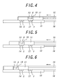
- Figs. 4-6 relate to another embodiment of the Si crystal thin film forming method of the present invention.
- an intended Si crystal thin film is formed by utilizing the sliding board.
- the second member 12 includes an additive element melt holder 17 in addition to the substrate holder 14.
- the first member 11 and the second member 12 are prepared so that the Si melt holder 13 is opposed to the additive element melt holder 17.
- the Si melt X is contacted to the additive element melt or the Si crystal with the additive element Y so that additive elements in the additive element melt or the Si crystal Y are contained in the Si melt X through convection and diffusion.
- the Si melt holder 13 is capped with the carbon or quartz cap 19.
- the Si melt X is heated to a given temperature above the Si melting point. Since the Si melt X contains the additive elements, in order to conduct the LPE in good condition, the first temperature at which the crystal growth starts is set within a temperature range between the Si melting point and-50°C of the Si melting point.
- the motor (not shown) is driven, and the first member 11 is slid in the left direction with the driving shaft 15 so that as illustrated in Fig. 5, the Si melt holder 13 is opposed to the Si substrate holder 14. Then, the Si substrate S is contacted to the Si melt X so that the intended Si crystal thin film is epitaxially grown on the Si substrate S.
- the first member 11 is slid in the left direction as illustrated in Fig. 6 so that the Si melt X is left away from the Si substrate S to terminate the LPE.
- the second temperature is preferably set within a temperature range between the Si melting point and -60°C of the Si melting point.
- the intended Si crystal thin film can be formed on the Si substrate by means of LPE.
- the thickness of the Si crystal thin film can be also varied by controlling the contacting period of time between the Si melt X and the Si substrate S and the temperature of the Si melt X.
- the Si crystal thin film contains the Ga additive element by 1 ⁇ 10 -9 -1 ⁇ 10 -2 at%.
- Fig. 7 relates to still another embodiment of the Si crystal thin film of the present invention.
- the Si melt X is charged into a given container 31, and the Si substrate is immersed into the Si melt X.
- the intended Si crystal thin film can be formed on the Si substrate through epitaxial growth.
- the thickness of the Si crystal thin film can be varied by controlling the temperature and the immersing period of time of the Si melt X. Moreover, at least one element selected from the group consisting of In, Ga, Sn, Al, Au-Bi and Cu can be added into the Si melt. In this case, too, the melting point (solidifying point) of the Si melt can be reduced, and the melting point zone can be enlarged. Therefore, in the LPE, the temperature control of the Si melt can be simplified, and the LPE can be conducted surely.
- an intended Si crystal thin film was formed according to the steps illustrated in Figs. 1-3.
- pure Si raw material was prepared and heated to 1450°C to form the Si melt X.
- the Si substrate S was made of metallurgical Si raw material.
- the Si melt X was kept at 1415°C, and as illustrated in Fig. 2, the Si substrate S was contacted to the Si melt X for about 0.5 ⁇ 1 minutes during cooling the Si melt at 1°C/min. to form the intended Si crystal thin film on the Si substrate S through LPE.
- the Si substrate S was left away from the Si melt X to terminate the LPE.
- the thickness of the Si crystal thin film was 50 ⁇ m, and the lifetime was 5 ⁇ s. Then, a solar battery was made of the Si crystal thin film, and it was turned out that the conversion efficiency of the solar battery was about 8% on the process of Bell Communications Research.
- the present invention was described in detail with reference to the above examples, this invention is not limited to the above disclosure and every kind of variation and modification may be made without departing from the scope of the present invention.
- the SiGe crystal thin film can be formed, instead of the Si crystal thin film.
- the present invention can be provided a forming technique of Si crystal thin film of low defect density and thus, high quality wherein expensive Si raw materials are not employed and whereby the high efficiency of a solar battery can be realized.
Landscapes
- Chemical & Material Sciences (AREA)
- Engineering & Computer Science (AREA)
- Crystallography & Structural Chemistry (AREA)
- Materials Engineering (AREA)
- Metallurgy (AREA)
- Organic Chemistry (AREA)
- Liquid Deposition Of Substances Of Which Semiconductor Devices Are Composed (AREA)
- Crystals, And After-Treatments Of Crystals (AREA)
- Photovoltaic Devices (AREA)
Applications Claiming Priority (2)
| Application Number | Priority Date | Filing Date | Title |
|---|---|---|---|
| JP2003167493 | 2003-06-12 | ||
| JP2003167493A JP3978494B2 (ja) | 2003-06-12 | 2003-06-12 | Si薄膜の作製方法 |
Publications (1)
| Publication Number | Publication Date |
|---|---|
| EP1487008A2 true EP1487008A2 (de) | 2004-12-15 |
Family
ID=33296867
Family Applications (1)
| Application Number | Title | Priority Date | Filing Date |
|---|---|---|---|
| EP04013647A Withdrawn EP1487008A2 (de) | 2003-06-12 | 2004-06-09 | Verfahren zur Herstellung eines Siliziumfilms, ein Siliziumfilm und eine Solarbatterie |
Country Status (3)
| Country | Link |
|---|---|
| US (1) | US20050034756A1 (de) |
| EP (1) | EP1487008A2 (de) |
| JP (1) | JP3978494B2 (de) |
Families Citing this family (1)
| Publication number | Priority date | Publication date | Assignee | Title |
|---|---|---|---|---|
| US9093705B2 (en) * | 2013-03-15 | 2015-07-28 | GM Global Technology Operations LLC | Porous, amorphous lithium storage materials and a method for making the same |
Family Cites Families (2)
| Publication number | Priority date | Publication date | Assignee | Title |
|---|---|---|---|---|
| JPS60145992A (ja) * | 1983-12-29 | 1985-08-01 | Sharp Corp | 炭化珪素単結晶基板の製造方法 |
| JP3478618B2 (ja) * | 1993-11-30 | 2003-12-15 | キヤノン株式会社 | 光電変換素子及びその製造方法 |
-
2003
- 2003-06-12 JP JP2003167493A patent/JP3978494B2/ja not_active Expired - Lifetime
-
2004
- 2004-06-04 US US10/860,060 patent/US20050034756A1/en not_active Abandoned
- 2004-06-09 EP EP04013647A patent/EP1487008A2/de not_active Withdrawn
Also Published As
| Publication number | Publication date |
|---|---|
| JP3978494B2 (ja) | 2007-09-19 |
| JP2005001945A (ja) | 2005-01-06 |
| US20050034756A1 (en) | 2005-02-17 |
Similar Documents
| Publication | Publication Date | Title |
|---|---|---|
| US5885345A (en) | Method of fabricating shaped crystals by overhead-pressure liquid injection | |
| CA1155735A (en) | Method for making silicon rods | |
| EP1634981A1 (de) | Indiumphosphidsubstrat, indiumphosphideinkristall und herstellungsverfahren dafür | |
| JP5111104B2 (ja) | SiドープGaAs単結晶インゴットおよびその製造方法 | |
| Capper | Bulk crystal growth: methods and materials | |
| CN101864593B (zh) | 掺氮晶体硅及其制备方法 | |
| US20090072205A1 (en) | Indium phosphide substrate, indium phosphide single crystal and process for producing them | |
| EP1487008A2 (de) | Verfahren zur Herstellung eines Siliziumfilms, ein Siliziumfilm und eine Solarbatterie | |
| US5612014A (en) | Compound semiconductor crystal | |
| JP2007019209A (ja) | 太陽電池用多結晶シリコンおよびその製造方法 | |
| JP4726454B2 (ja) | 多結晶シリコンインゴットの鋳造方法、これを用いた多結晶シリコンインゴット、多結晶シリコン基板、並びに太陽電池素子 | |
| JPH11147785A (ja) | 単結晶の製造方法 | |
| JP2003267717A (ja) | シリコンインゴットの製造方法および製造装置 | |
| EP1040212A1 (de) | Charge für tiegel im vertikalen wachsverfahren und deren verwendung | |
| JP2002029882A (ja) | 結晶成長自由表面を有する結晶製品及びその製造方法 | |
| US6497762B1 (en) | Method of fabricating crystal thin plate under micro-gravity environment | |
| JPH085760B2 (ja) | Hgl―xo Cdxo Te結晶インゴットの製造方法 | |
| JP2001267259A (ja) | 化合物半導体バルク結晶の成長方法、および化合物半導体装置の製造方法 | |
| JP2007045640A (ja) | 半導体バルク結晶の作製方法 | |
| JP2000154089A (ja) | るつぼ壁面被覆用b2o3材料及びその製造方法並びに、それを用いた単結晶製造方法及びその方法により製造された単結晶 | |
| JPH10298000A (ja) | 板状単結晶およびその製造方法 | |
| JPH10287492A (ja) | 硼酸リチウム単結晶の育成方法 | |
| JPH11130579A (ja) | 化合物半導体単結晶の製造方法及びその製造装置 | |
| Mullin | Compound semiconductor processing | |
| JP2004269328A (ja) | 単結晶の製造装置 |
Legal Events
| Date | Code | Title | Description |
|---|---|---|---|
| PUAI | Public reference made under article 153(3) epc to a published international application that has entered the european phase |
Free format text: ORIGINAL CODE: 0009012 |
|
| 17P | Request for examination filed |
Effective date: 20040609 |
|
| AK | Designated contracting states |
Kind code of ref document: A2 Designated state(s): AT BE BG CH CY CZ DE DK EE ES FI FR GB GR HU IE IT LI LU MC NL PL PT RO SE SI SK TR |
|
| AX | Request for extension of the european patent |
Extension state: AL HR LT LV MK |
|
| STAA | Information on the status of an ep patent application or granted ep patent |
Free format text: STATUS: THE APPLICATION HAS BEEN WITHDRAWN |
|
| 18W | Application withdrawn |
Effective date: 20050408 |