EP1486985A2 - Nonvolatile semiconductor memory device and control method thereof - Google Patents
Nonvolatile semiconductor memory device and control method thereof Download PDFInfo
- Publication number
- EP1486985A2 EP1486985A2 EP04253457A EP04253457A EP1486985A2 EP 1486985 A2 EP1486985 A2 EP 1486985A2 EP 04253457 A EP04253457 A EP 04253457A EP 04253457 A EP04253457 A EP 04253457A EP 1486985 A2 EP1486985 A2 EP 1486985A2
- Authority
- EP
- European Patent Office
- Prior art keywords
- voltage
- pulse
- programming
- memory cell
- erasing
- Prior art date
- Legal status (The legal status is an assumption and is not a legal conclusion. Google has not performed a legal analysis and makes no representation as to the accuracy of the status listed.)
- Granted
Links
Images








Classifications
-
- G—PHYSICS
- G11—INFORMATION STORAGE
- G11C—STATIC STORES
- G11C13/00—Digital stores characterised by the use of storage elements not covered by groups G11C11/00, G11C23/00, or G11C25/00
- G11C13/0002—Digital stores characterised by the use of storage elements not covered by groups G11C11/00, G11C23/00, or G11C25/00 using resistive RAM [RRAM] elements
- G11C13/0021—Auxiliary circuits
- G11C13/0069—Writing or programming circuits or methods
-
- G—PHYSICS
- G11—INFORMATION STORAGE
- G11C—STATIC STORES
- G11C11/00—Digital stores characterised by the use of particular electric or magnetic storage elements; Storage elements therefor
- G11C11/56—Digital stores characterised by the use of particular electric or magnetic storage elements; Storage elements therefor using storage elements with more than two stable states represented by steps, e.g. of voltage, current, phase, frequency
- G11C11/5685—Digital stores characterised by the use of particular electric or magnetic storage elements; Storage elements therefor using storage elements with more than two stable states represented by steps, e.g. of voltage, current, phase, frequency using storage elements comprising metal oxide memory material, e.g. perovskites
-
- G—PHYSICS
- G11—INFORMATION STORAGE
- G11C—STATIC STORES
- G11C13/00—Digital stores characterised by the use of storage elements not covered by groups G11C11/00, G11C23/00, or G11C25/00
- G11C13/0002—Digital stores characterised by the use of storage elements not covered by groups G11C11/00, G11C23/00, or G11C25/00 using resistive RAM [RRAM] elements
- G11C13/0007—Digital stores characterised by the use of storage elements not covered by groups G11C11/00, G11C23/00, or G11C25/00 using resistive RAM [RRAM] elements comprising metal oxide memory material, e.g. perovskites
-
- G—PHYSICS
- G11—INFORMATION STORAGE
- G11C—STATIC STORES
- G11C13/00—Digital stores characterised by the use of storage elements not covered by groups G11C11/00, G11C23/00, or G11C25/00
- G11C13/0002—Digital stores characterised by the use of storage elements not covered by groups G11C11/00, G11C23/00, or G11C25/00 using resistive RAM [RRAM] elements
- G11C13/0021—Auxiliary circuits
- G11C13/0064—Verifying circuits or methods
-
- G—PHYSICS
- G11—INFORMATION STORAGE
- G11C—STATIC STORES
- G11C5/00—Details of stores covered by group G11C11/00
- G11C5/06—Arrangements for interconnecting storage elements electrically, e.g. by wiring
- G11C5/063—Voltage and signal distribution in integrated semi-conductor memory access lines, e.g. word-line, bit-line, cross-over resistance, propagation delay
-
- G—PHYSICS
- G11—INFORMATION STORAGE
- G11C—STATIC STORES
- G11C13/00—Digital stores characterised by the use of storage elements not covered by groups G11C11/00, G11C23/00, or G11C25/00
- G11C13/0002—Digital stores characterised by the use of storage elements not covered by groups G11C11/00, G11C23/00, or G11C25/00 using resistive RAM [RRAM] elements
- G11C13/0021—Auxiliary circuits
- G11C13/0069—Writing or programming circuits or methods
- G11C2013/0071—Write using write potential applied to access device gate
-
- G—PHYSICS
- G11—INFORMATION STORAGE
- G11C—STATIC STORES
- G11C13/00—Digital stores characterised by the use of storage elements not covered by groups G11C11/00, G11C23/00, or G11C25/00
- G11C13/0002—Digital stores characterised by the use of storage elements not covered by groups G11C11/00, G11C23/00, or G11C25/00 using resistive RAM [RRAM] elements
- G11C13/0021—Auxiliary circuits
- G11C13/0069—Writing or programming circuits or methods
- G11C2013/009—Write using potential difference applied between cell electrodes
-
- G—PHYSICS
- G11—INFORMATION STORAGE
- G11C—STATIC STORES
- G11C2213/00—Indexing scheme relating to G11C13/00 for features not covered by this group
- G11C2213/30—Resistive cell, memory material aspects
- G11C2213/31—Material having complex metal oxide, e.g. perovskite structure
-
- G—PHYSICS
- G11—INFORMATION STORAGE
- G11C—STATIC STORES
- G11C2213/00—Indexing scheme relating to G11C13/00 for features not covered by this group
- G11C2213/70—Resistive array aspects
- G11C2213/79—Array wherein the access device being a transistor
Definitions
- the present invention relates to a nonvolatile semiconductor memory device having a memory array in which a plurality of memory cells each formed by connecting one end of a variable resistive element for storing information according to a change in electric resistance caused by application of a voltage and a drain of a selection transistor to each other on a semiconductor substrate are arranged in the row direction and the column direction, and a control method thereof. More particularly, the present invention relates to a method of applying a voltage to a memory cell at the time of programming or erasing.
- a nonvolatile semiconductor memory is becoming more and more important.
- power consumption of a logic circuit for executing a logic function is dominant but, in a standby state, power consumption of a memory device is dominant.
- the power consumption in the standby state is becoming more important as the drive time by a battery of a mobile apparatus increases.
- the nonvolatile semiconductor memory it becomes unnecessary to supply power to the nonvolatile semiconductor memory in the standby state, so that the power consumption can be reduced to the limit.
- Nonvolatile semiconductor memories include a flash memory, an FeRAM (Ferroelectric Random Access Memory) and the like, and many of them are already practically used. Those nonvolatile semiconductor memories have tradeoffs among high speed, rewrite resistance, power consumption and the like. Research and development for an ideal nonvolatile semiconductor memory satisfying all of required specifications are being conducted. Some nonvolatile semiconductor memories using new materials have been already proposed and an RRAM (Resistance Random Access Memory) is one of promising nonvolatile semiconductor memories. Since the RRAM has high potentials of high speed, large capacity, low power consumption and the like, expectations are placed on the future potential of the RRAM.
- RRAM Resistance Random Access Memory
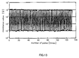
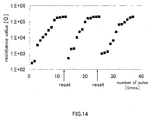
- FIG. 13 shows a change in the resistance value when a pulse of 100 nanoseconds of ⁇ 5 V is applied to the PCMO having a thickness of 100 nm.
- the resistance value changes between 1 k ⁇ and 1 M ⁇ and a large change of three digits in the resistance value occurs reversibly 100 times or more.
- the present invention has been made in consideration of the problems and its object is to provide a nonvolatile semiconductor memory device and a control method thereof which can realize reliable programming and erasing of data to/from a memory cell while suppressing increase in current consumption at the time of programming or erasing and in which a memory cell includes a variable resistive element for storing information according to a change in electric resistance caused by application of a voltage.
- the present invention provides a nonvolatile semiconductor memory device comprising at least: a memory array in which a plurality of memory cells are arranged in a row direction and a column direction, each of the memory cells being formed by connecting one end of a variable resistive element for storing information according to a change in electric resistance caused by an electric stress and a drain of a selection transistor to each other on a semiconductor substrate; a word line connected to gates of the selection transistors of the plurality of memory cells in the same row; a source line connected to sources of the selection transistors of the plurality of memory cells in the same row or the same column: a bit line connected to the other ends of the variable resistive elements of the plurality of memory cells in the same column; a control circuit for executing controls of programming, erasing and reading of information to/from the memory cell; a voltage switch circuit for switching among a program voltage, an erase voltage and a read voltage to be applied to the source line and the bit line; and a read circuit for reading information from the memory
- the present invention also provides a control method of a nonvolatile semiconductor memory device, wherein the nonvolatile semiconductor memory device comprises at least: a memory array in which a plurality of memory cells are arranged in a row direction and a column direction, each of the memory cells being formed by connecting one end of a variable resistive element for storing information according to a change in electric resistance caused by an electric stress and a drain of a selection transistor to each other on a semiconductor substrate; a word line connected to gates of the selection transistors of the plurality of memory cells in the same row; a source line connected to sources of the selection transistors of the plurality of memory cells in the same row or the same column; a bit line connected to the other ends of the variable resistive elements of the plurality of memory cells in the same column; a control circuit for executing controls of programming, erasing and reading of information to/from the memory cell; a voltage switch circuit for switching among a program voltage, an erase voltage and a read voltage to be applied to the source line
- a voltage pulse of a voltage value adjusted for programming is generated at the time of programming, and a voltage pulse of a voltage value adjusted for erasing is generated at the time of erasing.
- a voltage value obtained by subtracting a drain-source voltage of the selection transistor from an absolute value of a voltage difference between the program voltage or the erase voltage applied to the bit line and the source line is set to be larger than either a program threshold voltage necessary for programming data to the variable resistive element or an erase threshold voltage necessary for erasing data in the variable resistive element.
- the voltage value of the voltage pulse is set so that the selection transistor operates in a saturation region at least in a period in the application period of the voltage pulse when the voltage pulse is applied to the gate of the selection transistor of the memory cell to be programmed or erased.
- the program voltage or the erase voltage to be applied to the bit line and the source line is applied to the bit line or the source line and the word line
- the voltage pulse to be applied to the word line is applied to the source line or the bit line to which the program voltage or the erase voltage is not applied.
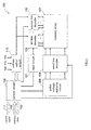
- FIG. 1 is a block diagram of an inventive device 100.
- the inventive device 100 has a configuration in that information is stored in a memory array 101 and the memory array 101 is constructed by arranging a plurality of memory cells. Information can be stored/read to/from a memory cell in the memory array 101.
- a word line decoder 104 selects a word line in the memory array 101 corresponding to a signal input to the address line 102
- a bit line decoder 105 selects a bit line in the memory array 101 corresponding to an address signal input to the address line 102
- a source line decoder 106 selects a source line of the memory array 101 corresponding to the address signal input to the address line 102.
- a control circuit 109 controls programming, erasing and reading of the memory array 101.
- the control circuit 109 controls the word line decoder 104, the bit line decoder 105, the source line decoder 106, a voltage switch circuit 110 and a pulse voltage applying circuit 108 on the basis of an address signal input from the address line 102, data input (at the time of programming) input from the data line 103 and a control input signal input from a control signal line 111, and controls reading, programming and erasing operations of the memory array 101.
- the control circuit 109 has, although not shown, functions of an address buffer circuit, a data input/output buffer circuit and a control input buffer circuit as general circuits.
- the voltage switch circuit 110 applies a bit line voltage and a source line voltage which are necessary at the time of reading, programming and erasing of the memory array 101.
- Vcc denotes a voltage supplied to the device.
- Vss denotes a ground voltage, and Vpp denotes a voltage for programming or erasing.
- the pulse voltage applying circuit 108 applies a pulse voltage to a word line selected by the word line decoder 104.
- the pulse voltage applying circuit 108 further has the function capable of simultaneously applying the same pulse voltage to one or more word lines and has the function capable of simultaneously applying a pulse voltage at different voltage levels to two or more word lines.
- Data is read from the memory array 101 via the bit line decoder 105 and a read circuit 107.
- the read circuit 107 determines the state of data, sends the result to the control circuit 109, and outputs it to the data line 103.
- FIG. 2 is a schematic cross-sectional view of a memory cell 11 as a component of the memory array 101.
- the memory cell 11 is formed by connecting a selection transistor 6 and a variable resistive element 10 in series while electrically connecting a drain region 3 and a lower electrode 7.
- the selection transistor 6 is constructed by a source region 2 and the drain region 3 made in a semiconductor substrate 1 and a gate electrode 5 formed on a gate oxide film 4.
- the variable resistive element 10 is constructed by sandwiching a variable resistive material 8 of which resistance value changes when a voltage is applied between the lower electrode 7 and an upper electrode 9.
- the upper electrode 9 is connected to a metal wire 12 serving as a bit line
- the gate electrode 5 is connected to a word line
- the source region 2 is connected to a diffusion layer or a metal wire 13 serving as a source line.
- the variable resistive element 10 is a nonvolatile memory element of which electric resistance changes by application of a voltage and, even after the application of the voltage is finished, whose changed electric resistance is held, and which can store data according to the resistance change, and is a CMR (Colossal Magnetoresistance) memory element made of an oxide having a perovskite type crystal structure containing manganese.
- the variable resistive material 8 for example, a film formed by using any of materials expressed as Pr 1-x Ca x MnO 3 , La 1-x Ca x MnO 3 (PCMO), or La 1-x-y Ca x Pb y MnO 3 (where x ⁇ 1, y ⁇ 1, x + y ⁇ 1) is used.
- a manganese oxide film made of Pr 0.7 Ca 0.3 MnO 3 , La 0.65 Ca 0.35 MnO 3 , La 0.65 Ca 0.175 Pb 0.175 MnO 3 or the like is formed by MOCVD, spin coating, laser ablation, sputtering or the like.
- variable resistive element 10 Since the resistance change of the variable resistive element 10 is as large as three digits or more, even when a resistance value is divided into a plurality of regions and different information is defined for the regions, each of the information can be sufficiently determined. Consequently, the variable resistive element 10 can store multivalue information of one bit (binary data) or more.
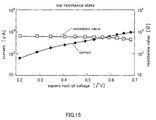
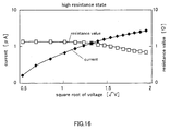
- the above-listed variable resistive materials have a non-linear current-voltage characteristic. Concretely, they have the Poole-Frenkele type nonlinear electric conductivity characteristic described above.
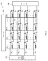
- FIGS. 3 and 4 schematically show the configurations of the memory array 101.
- the memory array 101 has a configuration in that mxn memory cells 11 are disposed at intersecting points of m bit lines (BL1 to BLm) and n word lines (WL1 to WLn).
- FIG. 3 shows a configuration in that n source lines (SL1 to SLn) are disposed in parallel with the word lines.
- FIG. 4 shows a configuration in that m source lines (SL1 to SLm) are disposed in parallel with bit lines.
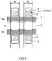
- FIG. 5 is a schematic view showing the layout of a part (four cells) of the memory array 101 in which the source lines are parallel with the word lines as shown in FIG. 3.
- FIG. 3 shows a configuration in that n source lines (SL1 to SLn) are disposed in parallel with the word lines.
- FIG. 4 shows a configuration in that m source lines (SL1 to SLm) are disposed in parallel with bit lines.
- FIG. 5 is a schematic view showing
- FIG. 6 is a schematic view showing the layout of a part (two cells) of the memory array in which the source lines are parallel with the bit lines as shown in FIG. 4.
- the memory arrays 101 in FIGS. 5 and 6 have different numbers of cells, but have almost the same area.
- the sectional structure of the memory cell shown in FIG. 2 does not directly correspond to any of the layouts of FIGS. 5 and 6, but can be adapted to the layout of each of the memory cells of FIGS. 5 and 6 by changing arrangement of the bit lines or source lines on the basis of the sectional structure of the memory cell shown in FIG. 2.
- the source line SL can be formed by a diffusion layer.
- the source line SL cannot be formed by the diffusion layer. It is necessary to provide a contact in a source diffusion region and connect the contact to the source line SL of a metal layer every two cells. Since the source line SL has to be formed between the bit lines BL, the cell area enlarges.
- the selection transistors 6 in not-selected cells in the same row and using a common word line are turned on and Vpp is applied to the source regions 2. Consequently, it becomes necessary to apply Vpp to all of bit lines of not-selected cells to prevent a voltage from being applied to the variable resistive elements 10, and the control becomes complicated.
- Any of the configurations of the memory array may be used, but it is preferable to use the array of FIG. 3 having a small cell area from the viewpoint of manufacturing cost.
- the present invention is not limited to the extending direction of the source lines, and the configurations of the memory array are not limited to the configurations shown in FIGS. 3 and 4, but a configuration obtained by modifying the two configurations may be also used.
- Table 1 shows voltage conditions at terminals at the time of programming and erasing of the memory cell 11.
- Vpp is applied to the upper electrode
- Vss is applied to the source region
- a voltage pulse having a voltage amplitude Vwp which will be described later is applied to the gate electrode and the selection transistor 6 is turned on
- a positive voltage which is equal to or more than a program threshold voltage switching voltage which changes from the low resistance state to the high resistance state is applied to the variable resistive element 10
- the low resistance state changes to the high resistance state (the voltage polarity in the case where the upper electrode has a voltage higher than that of the lower electrode is set to be positive).
- Vss is applied to the upper electrode
- Vpp is applied to the source region
- a voltage pulse having voltage amplitude Vwe is applied to the gate electrode
- the selection transistor 6 is turned on, a negative voltage whose absolute value is equal to or more than the erase threshold voltage is applied to the variable resistive element 10 and the variable resistive element 10 changes from the high resistance state to the low resistance state.
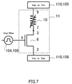
- the control method of the inventive device 100 will be described by also using an equivalent circuit of the memory cell 11 shown in FIG. 7.
- the selection transistor 6 and the variable resistive element 10 are connected in series, and the source region 2 in the selection transistor 6 and the upper electrode 9 of the variable resistive element 10 are connected to the voltage switch circuit 110 in FIG. 2, respectively.
- Vpp program or erase voltage
- Vss ground voltage
- the pulse voltage applying circuit 108 is connected to the gate electrode 5 of the selection transistor 6, and a pulse voltage having a pulse width of "t" seconds and a voltage amplitude of Vwp or Vwe can be applied to the gate electrode 5.
- the selection transistor 6 can be equivalently used as a resistive element 17 having an ON-state resistance value Ron and can be expressed as an equivalent circuit shown in FIG. 8.
- the resistance value of the variable resistive element 10 is expressed as Rr, and voltages to the resistive element 17 as the selection transistor 6 are described as Vds and Vr.
- the drain current does not show a large change in response to a change in the source-drain voltage Vds and the resistive element 17 can be dealt approximately as a constant current element.
- the selection transistor 6 operates in a linear region (non-saturation region)
- the drain current changes so as to follow a change in the source-drain voltage.
- Vpp Vpp ⁇ Rr /( Rr + Ron )
- Vds Vpp ⁇ Ron /( Rr + Ron )
- the voltage Vr applied to the variable resistive element 10 can be controlled as shown by Mathematical Expression (1). Consequently, the voltage pulse having the voltage amplitude Vwp adjusted so that a voltage which is equal to or more than the program threshold voltage and is close to the program threshold voltage as much as possible is applied to the variable resistive element 10 is applied to the gate electrode 5.
- Vr denotes a voltage applied across the upper electrode 9 and the lower electrode 7 when the same current as the drain current flowing in the selection transistor 6 flows in the variable resistive element 10.
- variable resistive element 10 If the voltage amplitude Vwp is increased unnecessarily and the on-state resistance Ron decreases excessively, a voltage exceeding the program threshold voltage is applied to the variable resistive element 10. Moreover, the drain current at the time of programming increases and, as a result, the current consumption at the time of programming increases.
- the erasing operation of the memory cell 11 is the same as the programming operation.
- the resistance value of the variable resistive element 10 in the memory cell 11 in the erasing operation is in the high resistance state, so that the erase threshold voltage can be applied to the variable resistive element 10 with a drain current smaller than that in the programming operation. Consequently, the on-state resistance Ron of the selection transistor 6 can be set to be higher than that in the programming operation, and the voltage amplitude Vwe of the pulse voltage applied to the gate electrode 5 has to be set to be smaller than the voltage amplitude Vwp in the programming operation.
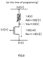
- FIG. 9 shows the voltages Vpp, Vss and Vwp applied to the terminals of the memory cell 11 in FIG. 7 in the programming operation, the drain-source voltage Vds, drain current and on-state resistance Ron of the selection transistor 6, and resistance Rr0 and a voltage Vr0 across terminals in the low resistance state of the variable resistive element 10.
- the voltages Vpp, Vss and Vwp are 5 V, 0 V and 5.5 V, respectively.
- Vds, the drain current and on-state resistance Ron of the selection transistor 6 are 3.6 V, 1.95 mA and 1.8 k ⁇ , respectively.
- the resistance Rr0 and the voltage Vr0 across the terminals of the variable resistive element 10 are 720 ⁇ and 1.4 V, respectively.
- the voltage amplitude Vwp of the pulse voltage is 5.5 V
- the voltage of 1.4 V exceeding the program threshold voltage is applied to the variable resistive element 10 and the resistance value changes from 720 ⁇ to the high resistance state.
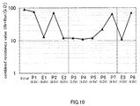
- FIG. 10 shows dependency of the voltage amplitude Vwp in the programming operation.
- the figure shows changes in a combined resistance value (Rr + Ron) of the memory cell 11 in the case where the programming/erasing operation is repeated from the left end to the right.
- a predetermined read voltage of 1 V or less is applied to a bit line, unnecessary programming and erasing operations are eliminated, and the combined resistance value is measured.
- P1 to P8 denote the programming operations
- E1 to E3 denote the erasing operations.
- Vpp and Vss in the programming and erasing operations are 5 V and 0 V, respectively, and the pulse width of the pulse voltage is 100 nanoseconds.
- the voltage values of the voltage amplitudes Vwp and Vwe of pulse voltages in the operations are shown in parentheses below P1 to P8 and E1 to E3.
- P1, E1, P2 and E2 show an operation check to see whether programming/erasing can be normally performed on the sample used for the program/erase test.
- the pulse voltage is applied while increasing the voltage amplitude Vwp step by step in increments of 0.5 V from 3.0 V to 5.5 V.
- programming with the voltage amplitude Vwp of 5.5 V could be checked.
- E3 and P8 denote an operation check made after the dependency of the voltage amplitude Vwp was examined.
- the voltage of 1.4 V exceeding the program threshold voltage is not applied to the variable resistive element 10 when the voltage amplitude Vwp is 5 V or less and the variable resistive element 10 does not change from the low resistance state (720 ⁇ ) to the high resistance state. Since intermediate programming is recognized when the voltage amplitude Vwp is 5 V, by controlling the voltage amplitude Vwp with high precision, multi-value storage can be realized.
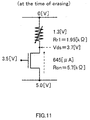
- FIG. 11 shows the voltages Vpp, Vss and Vwe applied to the terminals of the memory cell 11 in FIG. 7 in the erasing operation, the drain-source voltage Vds, drain current and on-state resistance Ron of the selection transistor 6, and resistance Rr1 and a voltage Vr1 across terminals in the high resistance state of the variable resistive element 10.
- the voltages Vpp, Vss and Vwe are 5 V, 0 V and 3.5 V, respectively.
- Vds, the drain current and on-state resistance Ron of the selection transistor 6 are 3.7 V, 645 ⁇ A, and 5.7 k ⁇ , respectively.
- the resistance Rr1 and the voltage Vr1 across the terminals (absolute value) of the variable resistive element 10 are 1.95 k ⁇ and 1.3 V, respectively.
- the voltage amplitude Vwe of the pulse voltage is 3.5 V
- the voltage of 1.4 V (absolute value) exceeding the erase threshold voltage is applied to the variable resistive element 10 and the resistance value changes from 1.95 k ⁇ to the low resistance state.
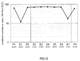
- FIG. 12 shows dependency of the voltage amplitude Vwe in the erasing operation.
- the figure shows changes in a combined resistance value (Rr + Ron) of the memory cell 11 in the case where the programming/erasing operation is repeated from the left end to the right.
- a predetermined read voltage of 1 V or less is applied to a bit line, unnecessary programming and erasing operations are eliminated, and the combined resistance value is measured.
- P1 to P3 denote the programming operations
- E1 to E7 denote the erasing operations.
- Vpp and Vss in the programming and erasing operations are 5 V and 0 V, respectively, and the pulse width of the pulse voltage is 100 nanoseconds.
- the voltage values of the voltage amplitudes Vwp and Vwe of pulse voltages in the operations are shown in parentheses below P1 to P3 and E1 to E7.
- P1, E1 and P2 show an operation check to see whether programming/erasing can be normally performed on the sample used for the program/erase test.
- the pulse voltage is applied while increasing the voltage amplitude Vwe step by step in increments of 0.5 V from 1.0 V to 3.5 V As a result, erasing with the voltage amplitude Vwe of 3.5 V could be checked.
- P3 denotes a program operation check made after the dependency of the voltage amplitude Vwe was examined.
- the gate voltage becomes dominant. Even when the drain-source voltage Vds changes, an almost constant drain current flows, so that constant current programming is performed.
- the drain current is adjusted with the voltage amplitude Vwp or Vwe of the pulse voltage, and the voltage value of Vr applied to the variable resistive element 6 can be changed.
- the selection transistor 6 operates in the non-saturation region, the drain-source voltage Vds becomes dominant, so that constant current programming is not performed.
- the drain-source voltage Vds becomes large to a certain extent, the linearity deteriorates, and the drain current changes due to a change in the gate voltage. Consequently, by adjusting the drain current by the voltage amplitude Vwp or Vwe of the pulse voltage, the voltage value of Vr applied to the variable resistive element 10 can be changed.
- the saturation region is desirable as the operation region when the pulse voltage is applied to the gate voltage 5 of the selection transistor 6.
- the resistance value of the variable resistive element 10 decreases and the drain current becomes higher as compared with that in the initial state. It is therefore preferable that increase in the current consumption can be suppressed by the constant current operation. Consequently, even if the selection transistor is not in the saturation region at the start of the erasing operation, as the resistance value of the variable resistive element 10 changes, the drain-source voltage Vds increases, the selection transistor 6 enters a saturation state, and the current consumption at the time of erasing can be suppressed by the constant current operation.
- the pulse width of the pulse voltage in the sample examples of FIGS. 10 and 12, 100 nanoseconds is set.
- an optimum value has to be employed according to the characteristics of the variable resistive element 10.
- 100 nanoseconds is preferable and a value in the range from 10 nanoseconds to 100 ⁇ s may be appropriately selected. If the programming/erasing operation is completed with the pulse width of 100 ⁇ s or less. the time is sufficiently shorter than the program time of the flash memory under the present circumferences.
- the programming and erasing operations can be performed at the time of programming and erasing.
- another control method of using the same voltage amplitude of the pulse voltage at the time of programming and erasing and adjusting the program or erase voltage Vpp to be applied to the bit line or source line so as to apply a proper voltage to the variable resistive element 10 in each of the programming and erasing operations can be also considered.
- the selection transistor 6 operates in the saturation region, even when Vpp is changed, the amount of current flowing in the variable resistive element 10 does not change largely, so that the voltage applied to the variable resistive element 10 does not change so much.
- the programming or erasing method by controlling Vpp there is the possibility in that programming or erasing is not performed due to variations in the program or erase threshold voltage in the variable resistive element 10.
- the drain current in the selection transistor 6 is changed by controlling the gate voltage of the selection transistor 6, a necessary voltage to be applied to the variable resistive element 10 can be properly controlled. Consequently, excessive current does not flow in the memory cell 11 and the voltage amplitudes Vwp and Vwe of the pulse voltage can be controlled so that the voltage which is equal to or more than the program/erase threshold voltage and is close to the program/erase threshold voltage as much as possible can be applied to the variable resistive element 10 with high precision.
- the inventive method is particularly effective to a variable resistive element having a nonlinear current-voltage characteristic since the necessary voltage to be applied to the variable resistive element 10 can be controlled with high precision. Moreover, according to the inventive method, by changing the magnitude of the voltage amplitude Vwp of the pulse voltage at the time of programming, the voltage to be applied to the variable resistive element 10 can be adjusted with high precision. Consequently, the present invention provides the programming method particularly effective to a multivalue memory cell as a memory cell sensitive to variations in the resistance value and to which multivalue information of one or more bits is programmed.
- the program voltage Vpp and the ground voltage Vss are applied to a selected bit line and a not-selected bit line, respectively, via the bit line decoder 105 and the voltage switch circuit 110, and the ground voltage Vss is applied to all of the source lines via the source line decoder 106 and the voltage switch circuit 110.
- the pulse voltage having the voltage amplitude Vwp is applied to a selected word line from the pulse voltage applying circuit 108 via the word line decoder 104.
- the ground voltage Vss and the erase voltage Vpp are applied to a selected bit line and a not-selected bit line, respectively, via the bit line decoder 105 and the voltage switch circuit 110.
- the erase voltage Vpp and the ground voltage Vss are applied to a selected source line and a not-selected source line, respectively, by using the source line decoder 106 and the voltage switch circuit 110.
- the pulse voltage having the voltage amplitude Vwe is applied from the pulse voltage applying circuit 108 to a selected word line via the word line decoder 104.
- the program voltage Vpp and the ground voltage Vss are applied to a selected bit line and a not-selected bit line, respectively, via the bit line decoder 105 and the voltage switch circuit 110, and the ground voltage Vss is applied to all of the source lines via the source line decoder 106 and the voltage switch 110.
- the pulse voltage having the voltage amplitude Vwp is applied to a selected word line from the pulse voltage applying circuit 108 via the word line decoder 104.
- the ground voltage Vss is applied to all of bit lines via the bit line decoder 105 and the voltage switch circuit 110, and the erase voltage Vpp and the ground voltage Vss are applied to a selected source line and a not-selected source line, respectively, via the source line decoder 106 and the voltage switch circuit 110.
- the pulse voltage having the voltage amplitude Vwe is applied from the pulse voltage applying circuit 108 to a selected word line via the word line decoder 104.
- the number of word lines to which the pulse voltage is applied may be one.
- the pulse voltage may be also applied simultaneously to two or more word lines in order to increase the program speed (program throughput) of the inventive device.
- the number of word lines to which the pulse voltage is to be applied is two or more, by applying the pulse voltage while changing the voltage amplitude Vwp of the pulse voltage, information of different levels can be simultaneously programmed into the multivalue memory cell.
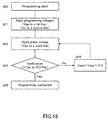
- step W1 Vpp and Vss are applied to a bit line and a source line, respectively, connected to the memory cell 11.
- step W2 the pulse voltage of Vwp is applied to the word line connected to the memory cell 11.
- a current value or a resistance value (combined resistance of a variable resistive element and a transistor) of the memory cell 11 is read, and whether the read value is equal to or less than a predetermined current value (Iw) or equal to or more than a predetermined resistance value (Rw) is verified (step W3), thereby indirectly determining whether the electric resistance of the variable resistive element 10 reaches a predetermined range (program state) or not. If the electric resistance has reached the range, the programming is finished (step W5). However, if the electric resistance has not reached the range yet, the word line voltage Vwp is increased only by ⁇ V (step W4), the pulse voltage is applied again (step W2) and, after that, similar verification is performed (step W3). The operation is repeated and application of the voltage pulse (step W2) and the verification (step W3) are performed until the electric resistance has reached the range, and the programming operation is finished.
- FIG. 10 shows the relation between the voltage amplitude Vwp at the time of programming of a pulse voltage to be applied to the gate voltage 5 of the selection transistor 6 and a read resistance value after application of the pulse voltage.
- the erasing operation can be also performed by a procedure similar to that of the programming operation.
- Vss and Vpp are applied to a bit line and a source line, respectively, connected to the memory cell 11.
- the pulse voltage of Vwe is applied to the word line connected to the memory cell 11.
- a current value or a resistance value (combined resistance of a variable resistive element and a selection transistor) of the memory cell 11 is read, and whether the read value is equal to or more than a predetermined current value (Ie) or equal to or less than a resistance value (Re) is verified (step E3), thereby indirectly determining whether the electric resistance of the variable resistive element 10 reaches a predetermined range (erase state) or not. If the electric resistance has reached the range, the erasing operation is finished (step E5). If the electric resistance has not reached the range yet, the word line voltage Vwe is increased only by ⁇ V (step E4), the pulse voltage is applied again (step E2) and, after that, similar verification is performed (step E3). The operation is repeated, application of the voltage pulse (step E2) and the verification (step E3) are performed until the electric resistance has reached the range, and the erasing operation is finished.
- FIG. 12 shows the relation between the voltage amplitude Vwe at the time of erasing with a pulse voltage to be applied to the gate voltage 5 of the selection transistor 6 and a read resistance value after application of the pulse voltage.
- the programming and erasing operations can be performed at the time of programming and erasing.
- the pulse width of the pulse voltage applied to the gate voltage 5 a period in which the memory cell is in the program or erase state is specified.
- the pulse voltage or erase voltage in pulses to be applied across a bit line and a source line in the first embodiment is applied.
- a predetermined word line voltage is applied to a word line connected to the memory cell to be programmed or erased, and the period in which the memory cell 11 enters the program or erase state is specified by the pulse width of a pulse voltage applied to either the bit line or the source line.
- FIG. 20 is a block diagram showing an inventive device 200 according to the second embodiment.
- a pulse voltage applying circuit 208 applies a pulse voltage to a bit line selected by the bit line decoder 105 or a source line selected by the source line decoder 106.
- the pulse voltage applying circuit 208 further has the function capable of applying the same pulse voltage to one or more bit lines or source lines and has the function capable of simultaneously applying pulse voltages of different voltage levels to two or more bit lines or source lines.
- a program voltage or erase voltage of the voltage switch circuit 110 is applied via the pulse voltage applying circuit 208.
- a predetermined word line voltage (Vwp in the programming operation and Vwe in the erasing operation) is applied by the word line decoder 104 via the voltage switch circuit 110, but is not applied as a pulse voltage specifying the program or erase period.
- the other circuit configuration is the same as that of the first embodiment and the same reference numeral is given to a circuit having the same function.
- the voltage switch circuit for word line voltage may be constructed by a circuit different from the voltage switch circuit for switching between the program voltage and the erase voltage of a bit line and a source line. In FIG. 20, both of the circuits are shown as one circuit.
- the program voltage Vwp and the ground voltage Vss are applied to a selected word line and a not-selected word line, respectively, via the word line decoder 104 and the voltage switch circuit 110.
- the ground voltage Vss is applied to all of source lines via the source line decoder 106 and the voltage switch circuit 110.
- the pulse voltage having the voltage amplitude Vpp is applied to a selected bit line via the bit line decoder 105 from the pulse voltage applying circuit 208.
- the ground voltage Vss and the erase voltage Vpp are applied to a selected bit line and a not-selected bit line, respectively, via the bit line decoder 105 and the voltage switch circuit 110.
- the erase voltage Vwe and the ground voltage Vss are applied to a selected word line and a not-selected source line, respectively, via the word line decoder 104 and the voltage switch circuit 110.
- the pulse voltage having the voltage amplitude Vpp is applied from the pulse voltage applying circuit 208 to a selected source line via the source line decoder 106.
- the program voltage Vwp and the ground voltage Vss are applied to a selected word line and a not-selected word line, respectively, via the word line decoder 104 and the voltage switch circuit 110, and the ground voltage Vss is applied to all of the source lines via the source line decoder 106 and the voltage switch circuit 110.
- the pulse voltage having the voltage amplitude Vpp is applied to a selected bit line from the pulse voltage applying circuit 208 via the bit line decoder 105.
- the ground voltage Vss is applied to all of bit lines via the bit line decoder 105 and the voltage switch circuit 110, the erase voltage Vwe and the ground voltage Vss are applied to a selected word line and a not-selected word line, respectively, via the word line decoder 104 and the voltage switch circuit 110, and the ground voltage Vss is applied to a not-selected source line via the source line decoder 106 and the voltage switch circuit 110.
- the pulse voltage having the voltage amplitude Vpp is applied from the pulse voltage applying circuit 208 to a selected source line via the source line decoder 106.
- the number of bit lines or source lines to which the pulse voltage is applied may be one.
- the pulse voltage may be also applied simultaneously to two or more bit lines or source lines in order to increase the program speed (program throughput) of the inventive device.
- the number of word lines to which the word line voltage is to be applied is two or more at the time of programming, by applying the word line voltage while changing the voltage amplitude Vwp of the word line voltage, information of different levels can be simultaneously programmed into the multivalue memory cell.
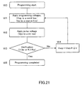
- step W1 Vwp and Vss are applied to a word line and a source line, respectively, connected to the memory cell 11.
- step W2 the pulse voltage of Vpp is applied to the bit line connected to the memory cell 11.
- a current value or a resistance value (combined resistance of a variable resistive element and a transistor) of the memory cell 11 is read, and whether the read value is equal to or less than a predetermined current value (Iw) or equal to or more than a predetermined resistance value (Rw) is verified (step W3), thereby indirectly determining whether the electric resistance of the variable resistive element 10 reaches a predetermined range (program state) or not. If the electric resistance reaches the range, the programming operation is finished (step W5). However, if the electric resistance does not satisfy the conditions, a voltage obtained by increasing the word line voltage Vwp only by ⁇ V in step W4 is applied to the word line in step W1.
- step W2 The pulse voltage is applied again to the bit line (step W2) and verification is performed similarly (step W3).
- step W3 The operation is repeated and application of the word line voltage (step W1), application of the voltage pulse (step W2) and verification (step W3) are performed until the electric resistance reaches the range, and the programming operation is finished.
- the erasing operation can be also performed by a procedure similar to that of the programming operation.
- Vwe and Vss are applied to a word line and a bit line, respectively, connected to the memory cell 11.
- the pulse voltage of Vpp is applied to the source line connected to the memory cell 11.
- a current value or a resistance value (combined resistance of a variable resistive element and a selection transistor) of the memory cell 11 is read, and whether the read value is equal to or less than a predetermined current value (Ie) or equal to or more than a resistance value (Re) is verified (step E3), thereby indirectly determining whether the electric resistance of the variable resistive element 10 reaches a predetermined range (erase state) or not. If the electric resistance has reached the range, the erasing is finished (step E5).
- step E1 If the electric resistance has not reached the range yet, a voltage obtained by increasing the word line voltage Vwe only by ⁇ V in step E4 is applied to the word line in step E1, the pulse voltage is applied again to the source line (step E2) and, after that, similar verification is performed (step E3). The operation is repeated and application of the word line voltage (step E1), application of the voltage pulse (step E2) and the verification (step E3) are performed until the electric resistance reaches the predetermined range, and the erasing operation is finished.
- the memory cell 11 is constructed as shown in FIGS. 2 and 7.
- the memory cell 11 may be also constructed in such a manner that the source region 2 of the selection transistor 6 and the lower electrode 7 of the variable resistive element 10 are electrically connected to each other, the upper electrode 9 is connected to a source line, the drain region 3 is connected to a bit line, and the position of the selection transistor 6 and that of the variable resistive element 10 are interchanged.
- the voltage difference (Vpp - Vss) between the upper electrode 9 and the drain region 3 is divided into the voltage Vr applied across both ends of the variable resistive element 10 and the source-drain voltage Vds in a normal state in a manner similar to the memory cell configurations shown in FIGS. 2 and 7.
- the inventive device and the inventive method are not limited to an RRAM using an oxide having a perovskite-type crystal structure containing manganese such as PCMO as the variable resistive material, but can be also easily applied to a nonvolatile semiconductor memory device in which a memory cell is constructed by using an element whose resistance value changes according to application of a voltage as a memory carrier.
- the nonvolatile semiconductor memory device and the control method thereof by applying voltages to a bit line and a source line and, after that, adjusting the voltage amplitude of a pulse voltage to be applied to a word line, the voltage applied to the variable resistive element can be adjusted with high precision. As a result, an excessive voltage is not applied to the variable resistive element at the time of programming/erasing, so that the programming and erasing operations can be performed with a small current amount. Since the voltage applied to the variable resistive element can be adjusted with high precision, the resistance value of the variable resistive element can be also controlled with high precision.
- the present invention can provide the nonvolatile semiconductor memory device and the control method thereof optimum to be used for a multivalue memory cell which is sensitive to variations in the resistance value and stores multivalue information of two or more bits.
- the amplitude of the word line voltage to be applied at the time of programming and erasing can be easily adjusted.
- the voltage applied to the variable resistive element can be adjusted with high precision.
- an excessive voltage is not applied to the variable resistive element, and programming and erasing can be performed with a small current amount.
Landscapes
- Engineering & Computer Science (AREA)
- Chemical & Material Sciences (AREA)
- Materials Engineering (AREA)
- Computer Hardware Design (AREA)
- Semiconductor Memories (AREA)
- Read Only Memory (AREA)
Abstract
Description
| Gate electrode | Upper electrode | Source region | |
| Program | Vwp | Vpp | Vss |
| Erase | Vwe | Vss | Vpp |
A predetermined read voltage of 1 V or less is applied to a bit line, unnecessary programming and erasing operations are eliminated, and the combined resistance value is measured. In the figure, P1 to P8 denote the programming operations and E1 to E3 denote the erasing operations. Vpp and Vss in the programming and erasing operations are 5 V and 0 V, respectively, and the pulse width of the pulse voltage is 100 nanoseconds. The voltage values of the voltage amplitudes Vwp and Vwe of pulse voltages in the operations are shown in parentheses below P1 to P8 and E1 to E3. P1, E1, P2 and E2 show an operation check to see whether programming/erasing can be normally performed on the sample used for the program/erase test. In the program operations P3 to P7, the pulse voltage is applied while increasing the voltage amplitude Vwp step by step in increments of 0.5 V from 3.0 V to 5.5 V. As a result, programming with the voltage amplitude Vwp of 5.5 V could be checked. E3 and P8 denote an operation check made after the dependency of the voltage amplitude Vwp was examined. It is therefore understood that the voltage of 1.4 V exceeding the program threshold voltage is not applied to the variable
A predetermined read voltage of 1 V or less is applied to a bit line, unnecessary programming and erasing operations are eliminated, and the combined resistance value is measured. In the figure, P1 to P3 denote the programming operations and E1 to E7 denote the erasing operations. Vpp and Vss in the programming and erasing operations are 5 V and 0 V, respectively, and the pulse width of the pulse voltage is 100 nanoseconds. The voltage values of the voltage amplitudes Vwp and Vwe of pulse voltages in the operations are shown in parentheses below P1 to P3 and E1 to E7.
P1, E1 and P2 show an operation check to see whether programming/erasing can be normally performed on the sample used for the program/erase test. In the erasing operations E2 to E7, the pulse voltage is applied while increasing the voltage amplitude Vwe step by step in increments of 0.5 V from 1.0 V to 3.5 V As a result, erasing with the voltage amplitude Vwe of 3.5 V could be checked. P3 denotes a program operation check made after the dependency of the voltage amplitude Vwe was examined. It is therefore understood that the voltage of 1.3 V (absolute value) exceeding the erase threshold voltage is not applied to the variable
Claims (29)
- A nonvolatile semiconductor memory device comprising at least:a memory array in which a plurality of memory cells are arranged in a row direction and a column direction, each of the memory cells being formed by connecting one end of a variable resistive element for storing information according to a change in electric resistance caused by an electric stress and a drain of a selection transistor to each other on a semiconductor substrate;a word line connected to gates of said selection transistors of said plurality of memory cells in the same row;a source line connected to sources of said selection transistors of said plurality of memory cells in the same row or the same column;a bit line connected to the other ends of said variable resistive elements of said plurality of memory cells in the same column;a control circuit for executing controls of programming, erasing and reading of information to/from said memory cell;a voltage switch circuit for switching among a program voltage, an erase voltage and a read voltage to be applied to said source line and said bit line: anda read circuit for reading information from said memory cell, characterized in thatthe nonvolatile semiconductor memory device further comprises a pulse voltage applying circuit for applying a voltage pulse for programming or erasing to said word line connected to the memory cell in the state where said program voltage or erase voltage corresponding to said bit line and said source line is applied to said bit line and said source line connected to said memory cell to be programmed or erased in said memory array via said voltage switch circuit.
- The nonvolatile semiconductor memory device according to claim 1, characterized in that
said pulse voltage applying circuit generates a voltage pulse of a voltage value adjusted for programming at the time of programming and generates a voltage pulse of a voltage value adjusted for erasing at the time of erasing. - The nonvolatile semiconductor memory device according to claim 2, characterized in that
when said voltage pulse generated by said pulse voltage applying circuit is applied to the gate of said selection transistor in said memory cell to be programmed or erased, a voltage value obtained by subtracting a drain-source voltage of the selection transistor from an absolute value of a voltage difference between said program voltage or said erase voltage applied to said bit line and said source line is set to be larger than either a program threshold voltage necessary for programming data to said variable resistive element or an erase threshold voltage necessary for erasing data in said variable resistive element. - The nonvolatile semiconductor memory device according to claim 2, characterized in that
the voltage value of said voltage pulse is set so that said selection transistor operates in a saturation region at least in a period in the application period of said voltage pulse when said voltage pulse is applied to the gate of said selection transistor of said memory cell to be programmed or erased. - The nonvolatile semiconductor memory device according to claim 1, characterized in that
said pulse voltage applying circuit has the function capable of simultaneously applying said voltage pulse to one or more said word lines. - The nonvolatile semiconductor memory device according to claim 1, characterized in that
said pulse voltage applying circuit has the function capable of simultaneously applying said voltage pulses of different voltage values to at least two said word lines at the time of programming. - A nonvolatile semiconductor memory device comprising at least:a memory array in which a plurality of memory cells are arranged in a row direction and a column direction, each of the memory cells being formed by connecting one end of a variable resistive element for storing information according to a change in electric resistance caused by an electric stress and a drain of a selection transistor to each other on a semiconductor substrate;a word line connected to gates of said selection transistors of said plurality of memory cells in the same row;a source line connected to sources of said selection transistors of said plurality of memory cells in the same row or the same column;a bit line connected to the other ends of said variable resistive elements of said plurality of memory cells in the same column;a control circuit for executing controls of programming, erasing and reading of information to/from said memory cell;a voltage switch circuit for switching among a program voltage, an erase voltage and a read voltage to be applied to said word line, said source line and said bit line; anda read circuit for reading information from said memory cell, characterized in thatthe nonvolatile semiconductor memory device further comprises a pulse voltage applying circuit for applying a voltage pulse for programming or erasing to said bit line or said source line which is connected to the memory cell and to which said program voltage or erase voltage is not applied in the state where said program voltage or erase voltage is applied to one of said bit line and said source line and said word line connected to said memory cell to be programmed or erased in said memory array via said voltage switch circuit.
- The nonvolatile semiconductor memory device according to claim 7, characterized in that
said pulse voltage applying circuit has the function capable of simultaneously applying said voltage pulse to one or more said bit lines or source lines. - The nonvolatile semiconductor memory device according to claim 7, characterized in that
means for applying said program voltage to said word line has the function capable of simultaneously applying said program voltages of different voltage values to at least two said word lines at the time of programming. - The nonvolatile semiconductor memory device according to claim 1 or 7, characterized in that
said variable resistive element is made of an oxide having a perovskite-type crystal structure containing manganese. - The nonvolatile semiconductor memory device according to claim 1 or 7, characterized in that
a current-voltage characteristic of said variable resistive element has a Poole-Frenkele type nonlinear electric conduction characteristic. - The nonvolatile semiconductor memory device according to claim 1 or 7, characterized in that
said source line and said bit line are disposed in parallel with each other in said memory cell. - The nonvolatile semiconductor memory device according to claim 1 or 7, characterized in that
said source line and said word line are disposed in parallel with each other in said memory cell. - The nonvolatile semiconductor memory device according to claim 1 or 7, characterized in that
said variable resistive element can store information of two or more values which can be read. - A control method of a nonvolatile semiconductor memory device, wherein
said nonvolatile semiconductor memory device comprises at least:a memory array in which a plurality of memory cells are arranged in a row direction and a column direction, each of the memory cells being formed by connecting one end of a variable resistive element for storing information according to a change in electric resistance caused by an electric stress and a drain of a selection transistor to each other on a semiconductor substrate;a word line connected to gates of said selection transistors of said plurality of memory cells in the same row;a source line connected to sources of said selection transistors of said plurality of memory cells in the same row or the same column;a bit line connected to the other ends of said variable resistive elements of said plurality of memory cells in the same column;a control circuit for executing controls of programming, erasing and reading of information to/from said memory cell;a voltage switch circuit for switching among a program voltage, an erase voltage and a read voltage to be applied to said source line and said bit line; anda read circuit for reading information from said memory cell, characterized in thatin the state where said program voltage or erase voltage corresponding to said bit line and said source line is applied to said bit line and said source line connected to said memory cell to be programmed or erased in said memory array via said voltage switch circuit, a voltage pulse for programming or erasing is applied to said word line connected to the memory cell, and a programming or erasing operation is performed. - The control method according to claim 15, characterized by comprising:a first step of applying a voltage pulse for programming or erasing to said word line connected to said memory cell in the state where said program voltage or erase voltage corresponding to said bit line and said source line is applied to said bit line and said source line connected to said memory cell to be programmed or erased in said memory array via said voltage switch circuit;a second step of determining whether electric resistance of said variable resistive element in said memory cell reaches a predetermined range or not;a third step of performing application of voltage again in said first step under a voltage application condition different from that in said first step in the case where said electric resistance has not reached said predetermined range; anda fourth step of repeating said second and third steps until said electric resistance reaches said predetermined range.
- The control method according to claim 16, characterized in that
the voltage amplitude of said voltage pulse in said third step is larger than that in said first step. - The control method according to claim 15, characterized in that
in the case of applying a voltage pulse for programming or erasing to said word line, a voltage pulse of a voltage value adjusted for programming is generated at the time of programming, and a voltage pulse of a voltage value adjusted for erasing is generated at the time of erasing. - The control method according to claim 18, characterized in that
when said voltage pulse is applied to the gate of said selection transistor in said memory cell to be programmed or erased, a voltage value obtained by subtracting a drain-source voltage of the selection transistor from an absolute value of a voltage difference between said program voltage or said erase voltage applied to said bit line and said source line is set to be larger than either a program threshold voltage necessary for programming data to said variable resistive element or an erase threshold voltage necessary for erasing data in said variable resistive element. - The control method according to claim 18, characterized in that
the voltage value of said voltage pulse is set so that said selection transistor operates in a saturation region at least in a period in the application period of said voltage pulse when said voltage pulse is applied to the gate of said selection transistor of said memory cell to be programmed or erased. - The control method according to claim 15, characterized in that
means for applying said voltage pulse to said word line simultaneously applies said voltage pulse to one or more said word lines. - The control method according to claim 15, characterized in that
at the time of programming, the means for applying said voltage pulse to said word line simultaneously applies said voltage pulses of voltage values respectively selected among a plurality of voltage values to two or more said word lines. - A control method of a nonvolatile semiconductor memory device, wherein
said nonvolatile semiconductor memory device comprises at least:a memory array in which a plurality of memory cells are arranged in a row direction and a column direction, each of the memory cells being formed by connecting one end of a variable resistive element for storing information according to a change in electric resistance caused by an electric stress and a drain of a selection transistor to each other on a semiconductor substrate;a word line connected to gates of said selection transistors of said plurality of memory cells in the same row;a source line connected to sources of said selection transistors of said plurality of memory cells in the same row or the same column;a bit line connected to the other ends of said variable resistive elements of said plurality of memory cells in the same column;a control circuit for executing controls of programming, erasing and reading of information to/from said memory cell;a voltage switch circuit for switching among a program voltage, an erase voltage and a read voltage to be applied to said word line, said source line and said bit line; anda read circuit for reading information from said memory cell, characterized in thatin the state where said program voltage or erase voltage is applied to one of said bit line and said source line and said word line connected to said memory cell to be programmed or erased in said memory array via said voltage switch circuit, a voltage pulse for programming or erasing is applied to said bit line or said source line which is connected to the memory cell and to which said program voltage or erase voltage is not applied, and a programming or erasing operation is performed. - The control method according to claim 23, characterized in that
means for applying said voltage pulse to said bit line or said source line simultaneously applies said voltage pulse to one or more bit lines or source lines. - The control method according to claim 23, characterized in that
means for applying said program voltage to said word line simultaneously applies said program voltages of different voltage values respectively selected from a plurality of voltage values to at least two said word lines at the time of programming. - The control method according to claim 23, characterized by comprising:a first step of applying a voltage pulse for programming or erasing to said bit line or said source line which is connected to said memory cell and to which said program voltage or erase voltage is not applied in the state where said program voltage or erase voltage corresponding to said bit line or said source line is applied to one of the said bit line and said source line and said word line connected to the memory cell to be programmed or erased in said memory array via said voltage switch circuit;a second step of determining whether electric resistance of said variable resistive element in said memory cell reaches a predetermined range or not;a third step of performing application of voltage again in said first step under a voltage application condition different from that in said first step in the case where said electric resistance has not reached said predetermined range; anda fourth step of repeating said second and third steps until said electric resistance reaches said predetermined range.
- The control method according to claim 26, characterized in that
the voltage applied to said word line in said third step is larger than that in said first step. - The control method according to claim 15 or 23, characterized in that
said variable resistive element can store information of two or more values which can be read. - The control method according to claim 15 or 23, characterized in that
a pulse time width of said voltage pulse is equal to or less than 100 microseconds and is equal to or more than 10 nanoseconds.
Applications Claiming Priority (4)
| Application Number | Priority Date | Filing Date | Title |
|---|---|---|---|
| JP2003168223 | 2003-06-12 | ||
| JP2003168223 | 2003-06-12 | ||
| JP2003433815A JP4113493B2 (en) | 2003-06-12 | 2003-12-26 | Nonvolatile semiconductor memory device and control method thereof |
| JP2003433815 | 2003-12-26 |
Publications (3)
| Publication Number | Publication Date |
|---|---|
| EP1486985A2 true EP1486985A2 (en) | 2004-12-15 |
| EP1486985A3 EP1486985A3 (en) | 2005-08-24 |
| EP1486985B1 EP1486985B1 (en) | 2007-09-12 |
Family
ID=33302293
Family Applications (1)
| Application Number | Title | Priority Date | Filing Date |
|---|---|---|---|
| EP04253457A Expired - Lifetime EP1486985B1 (en) | 2003-06-12 | 2004-06-10 | Nonvolatile semiconductor memory device and control method thereof |
Country Status (7)
| Country | Link |
|---|---|
| US (1) | US6995999B2 (en) |
| EP (1) | EP1486985B1 (en) |
| JP (1) | JP4113493B2 (en) |
| KR (1) | KR100547969B1 (en) |
| CN (1) | CN100479057C (en) |
| DE (1) | DE602004008833T2 (en) |
| TW (1) | TWI237271B (en) |
Cited By (10)
| Publication number | Priority date | Publication date | Assignee | Title |
|---|---|---|---|---|
| EP1612805A1 (en) * | 2004-06-30 | 2006-01-04 | Sharp Kabushiki Kaisha | Writing method of variable resistance memory device |
| WO2006035326A1 (en) * | 2004-09-30 | 2006-04-06 | Koninklijke Philips Electronics N.V. | Integrated circuit with memory cells comprising a programmable resistor and method for addressing memory cells comprising a programmable resistor |
| EP1557841A3 (en) * | 2004-01-20 | 2006-10-25 | Sony Corporation | Multilevel Resistive Memory device and its writing erasing method |
| WO2006137111A1 (en) | 2005-06-20 | 2006-12-28 | Fujitsu Limited | Nonvolatile semiconductor storage device and write method therefor |
| DE102005053496A1 (en) * | 2005-11-09 | 2007-05-10 | Infineon Technologies Ag | Memory unit e.g. programmable read only memory unit, has bit line, ground line and memory cells, which are assigned to transistors, where bit line and ground line run parallel to each other |
| WO2008082852A1 (en) * | 2006-12-29 | 2008-07-10 | Spansion Llc | Multibits resistance changing memory cell architecture and its writing method |
| EP1986196A1 (en) * | 2007-04-24 | 2008-10-29 | MagIC Technologies Inc. | A spin-torque MRAM: spin-RAM, array |
| US7463507B2 (en) | 2005-11-09 | 2008-12-09 | Ulrike Gruening-Von Schwerin | Memory device with a plurality of memory cells, in particular PCM memory cells, and method for operating such a memory cell device |
| US7643328B2 (en) | 2005-10-19 | 2010-01-05 | Fujitsu Limited | Method of writing into semiconductor memory device |
| EP2186095A4 (en) * | 2007-10-17 | 2010-12-01 | Toshiba Kk | Nonvolatile semiconductor memory device |
Families Citing this family (129)
| Publication number | Priority date | Publication date | Assignee | Title |
|---|---|---|---|---|
| US6962648B2 (en) * | 2003-09-15 | 2005-11-08 | Global Silicon Net Corp. | Back-biased face target sputtering |
| JP5135406B2 (en) * | 2004-02-20 | 2013-02-06 | ルネサスエレクトロニクス株式会社 | Semiconductor device |
| US7443710B2 (en) * | 2004-09-28 | 2008-10-28 | Spansion, Llc | Control of memory devices possessing variable resistance characteristics |
| US20060081467A1 (en) * | 2004-10-15 | 2006-04-20 | Makoto Nagashima | Systems and methods for magnetron deposition |
| US7425504B2 (en) * | 2004-10-15 | 2008-09-16 | 4D-S Pty Ltd. | Systems and methods for plasma etching |
| US20060081466A1 (en) * | 2004-10-15 | 2006-04-20 | Makoto Nagashima | High uniformity 1-D multiple magnet magnetron source |
| US7359236B2 (en) * | 2005-03-11 | 2008-04-15 | Adesto Technologies | Read, write and erase circuit for programmable memory devices |
| JP4552745B2 (en) * | 2005-05-10 | 2010-09-29 | ソニー株式会社 | Memory element and manufacturing method thereof |
| JP4313372B2 (en) * | 2005-05-11 | 2009-08-12 | シャープ株式会社 | Nonvolatile semiconductor memory device |
| KR100937564B1 (en) | 2005-06-20 | 2010-01-19 | 후지쯔 가부시끼가이샤 | Nonvolatile Semiconductor Memory and Writing Method Thereof |
| US7289351B1 (en) * | 2005-06-24 | 2007-10-30 | Spansion Llc | Method of programming a resistive memory device |
| JP2007018615A (en) * | 2005-07-08 | 2007-01-25 | Sony Corp | Memory device and semiconductor device |
| US7426128B2 (en) * | 2005-07-11 | 2008-09-16 | Sandisk 3D Llc | Switchable resistive memory with opposite polarity write pulses |
| JP4802608B2 (en) * | 2005-08-19 | 2011-10-26 | ソニー株式会社 | Storage device |
| JP4828901B2 (en) * | 2005-09-22 | 2011-11-30 | 株式会社東芝 | Semiconductor integrated circuit device |
| JP2007095131A (en) * | 2005-09-27 | 2007-04-12 | Oki Electric Ind Co Ltd | Nonvolatile semiconductor memory apparatus and data write-in method |
| US7514706B2 (en) * | 2005-10-14 | 2009-04-07 | Adesto Technologies | Voltage reference circuit using programmable metallization cells |
| US20070084717A1 (en) * | 2005-10-16 | 2007-04-19 | Makoto Nagashima | Back-biased face target sputtering based high density non-volatile caching data storage |
| US7286395B2 (en) * | 2005-10-27 | 2007-10-23 | Grandis, Inc. | Current driven switched magnetic storage cells having improved read and write margins and magnetic memories using such cells |
| DE102005063435B4 (en) * | 2005-11-09 | 2015-12-10 | Polaris Innovations Ltd. | Memory device with a plurality of memory cells, in particular PCM memory cells, and method for operating such a memory device |
| JP4764142B2 (en) | 2005-11-11 | 2011-08-31 | 株式会社東芝 | Semiconductor memory device |
| WO2007074504A1 (en) * | 2005-12-26 | 2007-07-05 | Fujitsu Limited | Nonvolatile semiconductor storage device and method for writing threrin |
| JP4203506B2 (en) * | 2006-01-13 | 2009-01-07 | シャープ株式会社 | Nonvolatile semiconductor memory device and rewriting method thereof |
| JP4594878B2 (en) * | 2006-02-23 | 2010-12-08 | シャープ株式会社 | Resistance control method for variable resistance element and nonvolatile semiconductor memory device |
| JP2007234133A (en) * | 2006-03-01 | 2007-09-13 | Matsushita Electric Ind Co Ltd | Semiconductor memory device and semiconductor integrated circuit system |
| US7522444B2 (en) | 2006-03-13 | 2009-04-21 | Infineon Technologies Ag | Memory circuit, method for operating a memory circuit, memory device and method for producing a memory device |
| KR100868035B1 (en) * | 2006-03-13 | 2008-11-10 | 키몬다 아게 | Memory circuit, method for operating a memory circuit, memory device and method for producing a memory device |
| EP1835509A1 (en) * | 2006-03-14 | 2007-09-19 | Qimonda AG | Memory cells, memory with a memory cell and method for writing data to a memory cell |
| US8395199B2 (en) * | 2006-03-25 | 2013-03-12 | 4D-S Pty Ltd. | Systems and methods for fabricating self-aligned memory cell |
| JP2007294592A (en) | 2006-04-24 | 2007-11-08 | Sony Corp | Driving method of storage device |
| WO2007132525A1 (en) * | 2006-05-16 | 2007-11-22 | Fujitsu Limited | Nonvolatile semiconductor memory device, and its writing method |
| US8014199B2 (en) * | 2006-05-22 | 2011-09-06 | Spansion Llc | Memory system with switch element |
| WO2007145295A1 (en) * | 2006-06-16 | 2007-12-21 | Panasonic Corporation | Nonvolatile memory device |
| JP4460552B2 (en) * | 2006-07-04 | 2010-05-12 | シャープ株式会社 | Semiconductor memory device |
| US20080011603A1 (en) * | 2006-07-14 | 2008-01-17 | Makoto Nagashima | Ultra high vacuum deposition of PCMO material |
| US7932548B2 (en) * | 2006-07-14 | 2011-04-26 | 4D-S Pty Ltd. | Systems and methods for fabricating self-aligned memory cell |
| US8454810B2 (en) * | 2006-07-14 | 2013-06-04 | 4D-S Pty Ltd. | Dual hexagonal shaped plasma source |
| US7428163B2 (en) * | 2006-07-21 | 2008-09-23 | Infineon Technologies Ag | Method and memory circuit for operating a resistive memory cell |
| JP4195715B2 (en) | 2006-07-31 | 2008-12-10 | シャープ株式会社 | Semiconductor memory device |
| JP4344372B2 (en) | 2006-08-22 | 2009-10-14 | シャープ株式会社 | Semiconductor memory device and driving method thereof |
| KR100755409B1 (en) * | 2006-08-28 | 2007-09-04 | 삼성전자주식회사 | How to Program a Resistive Memory Device |
| EP1898426A3 (en) * | 2006-09-05 | 2008-05-21 | Stmicroelectronics Sa | Phase-change memory erasable and programmable with the help of a line decoder |
| JP4823316B2 (en) * | 2006-09-05 | 2011-11-24 | 富士通株式会社 | Writing method for nonvolatile semiconductor memory device |
| KR100809337B1 (en) | 2006-09-06 | 2008-03-05 | 삼성전자주식회사 | Nonvolatile Memory Device and Driving Method thereof |
| US8308915B2 (en) | 2006-09-14 | 2012-11-13 | 4D-S Pty Ltd. | Systems and methods for magnetron deposition |
| KR101258983B1 (en) * | 2006-09-19 | 2013-04-29 | 삼성전자주식회사 | Semiconductor memory device using variable resistive element and operating method for thereof |
| US20080101110A1 (en) * | 2006-10-25 | 2008-05-01 | Thomas Happ | Combined read/write circuit for memory |
| US7920402B2 (en) | 2006-11-17 | 2011-04-05 | Panasonic Corporation | Resistance variable memory apparatus |
| JP2008146740A (en) | 2006-12-08 | 2008-06-26 | Sharp Corp | Semiconductor memory device |
| JP4745956B2 (en) * | 2006-12-25 | 2011-08-10 | 富士通株式会社 | Simulation device |
| JP4221031B2 (en) | 2007-02-09 | 2009-02-12 | シャープ株式会社 | Nonvolatile semiconductor memory device and rewriting method thereof |
| US8094481B2 (en) | 2007-03-13 | 2012-01-10 | Panasonic Corporation | Resistance variable memory apparatus |
| US7764537B2 (en) * | 2007-04-05 | 2010-07-27 | Qualcomm Incorporated | Spin transfer torque magnetoresistive random access memory and design methods |
| JP4288376B2 (en) | 2007-04-24 | 2009-07-01 | スパンション エルエルシー | Nonvolatile memory device and control method thereof |
| JP2008276858A (en) * | 2007-04-27 | 2008-11-13 | Spansion Llc | Nonvolatile storage device and bias control method therefor |
| WO2008149493A1 (en) * | 2007-06-01 | 2008-12-11 | Panasonic Corporation | Resistance change type memory |
| KR100914267B1 (en) * | 2007-06-20 | 2009-08-27 | 삼성전자주식회사 | Variable resistance memory device and its formation method |
| KR20090009699A (en) * | 2007-07-20 | 2009-01-23 | 삼성전자주식회사 | Semiconductor memory device having a capacitorless dynamic memory cell, dynamic memory cell for the device, and memory system having the device |
| US9129845B2 (en) | 2007-09-19 | 2015-09-08 | Micron Technology, Inc. | Buried low-resistance metal word lines for cross-point variable-resistance material memories |
| JP5050813B2 (en) * | 2007-11-29 | 2012-10-17 | ソニー株式会社 | Memory cell |
| JP2009141225A (en) | 2007-12-07 | 2009-06-25 | Sharp Corp | Variable resistance element, variable resistance element manufacturing method, and nonvolatile semiconductor memory device |
| JP5072564B2 (en) * | 2007-12-10 | 2012-11-14 | 株式会社東芝 | Semiconductor memory device and memory cell voltage application method |
| JP4356786B2 (en) * | 2007-12-12 | 2009-11-04 | ソニー株式会社 | Storage device and information re-recording method |
| JP2009146478A (en) * | 2007-12-12 | 2009-07-02 | Sony Corp | Storage device and information re-recording method |
| JP4607252B2 (en) | 2008-02-25 | 2011-01-05 | パナソニック株式会社 | Driving method of variable resistance element and variable resistance memory device using the same |
| US8094485B2 (en) | 2008-05-22 | 2012-01-10 | Panasonic Corporation | Variable resistance nonvolatile storage device with oxygen-deficient oxide layer and asymmetric substrate bias effect |
| JP5221222B2 (en) * | 2008-06-25 | 2013-06-26 | 株式会社東芝 | Semiconductor memory device |
| JP4555397B2 (en) | 2008-08-20 | 2010-09-29 | パナソニック株式会社 | Variable resistance nonvolatile memory device |
| US7889572B2 (en) * | 2008-09-04 | 2011-02-15 | Macronix International Co., Ltd. | Memory with high reading performance and reading method thereof |
| WO2010038442A1 (en) | 2008-09-30 | 2010-04-08 | パナソニック株式会社 | Method for driving resistance change element, initial processing method, and nonvolatile storage device |
| CN101933096A (en) * | 2008-10-21 | 2010-12-29 | 松下电器产业株式会社 | Non-volatile storage device and method for writing to its storage unit |
| CN101946285A (en) | 2008-12-18 | 2011-01-12 | 松下电器产业株式会社 | Nonvolatile storage device and method for writing into the same |
| JP4720912B2 (en) * | 2009-01-22 | 2011-07-13 | ソニー株式会社 | Resistance change memory device |
| KR101566899B1 (en) * | 2009-02-26 | 2015-11-06 | 삼성전자주식회사 | Semiconductor device and method for changing operating characteristics and semiconductor system having the same |
| JP4806046B2 (en) * | 2009-03-16 | 2011-11-02 | 株式会社東芝 | Semiconductor memory device |
| JP2010225227A (en) * | 2009-03-23 | 2010-10-07 | Toshiba Corp | Nonvolatile semiconductor memory device |
| WO2010109803A1 (en) | 2009-03-25 | 2010-09-30 | パナソニック株式会社 | Resistance-change non-volatile memory device |
| US7983065B2 (en) | 2009-04-08 | 2011-07-19 | Sandisk 3D Llc | Three-dimensional array of re-programmable non-volatile memory elements having vertical bit lines |
| US8351236B2 (en) * | 2009-04-08 | 2013-01-08 | Sandisk 3D Llc | Three-dimensional array of re-programmable non-volatile memory elements having vertical bit lines and a single-sided word line architecture |
| KR101717798B1 (en) * | 2009-04-08 | 2017-03-17 | 샌디스크 테크놀로지스 엘엘씨 | Three-dimensional array of re-programmable nonvolatile memory elements having vertical bit lines and a double-global-bit-line architecture |
| US8199576B2 (en) * | 2009-04-08 | 2012-06-12 | Sandisk 3D Llc | Three-dimensional array of re-programmable non-volatile memory elements having vertical bit lines and a double-global-bit-line architecture |
| JP4643767B2 (en) | 2009-04-15 | 2011-03-02 | パナソニック株式会社 | Variable resistance nonvolatile memory device |
| US8508976B2 (en) | 2009-04-30 | 2013-08-13 | Panasonic Corporation | Nonvolatile memory element and nonvolatile memory device |
| CN102077297A (en) | 2009-05-14 | 2011-05-25 | 松下电器产业株式会社 | Nonvolatile memory device and method for writing data to nonvolatile memory device |
| CN102099863B (en) * | 2009-06-08 | 2014-04-02 | 松下电器产业株式会社 | Method of writing for resistance-change non-volatile memory element, and resistance-change non-volatile memory device |
| CN102414819A (en) * | 2009-11-02 | 2012-04-11 | 松下电器产业株式会社 | Variable resistance non-volatile memory device, and method of forming memory cell |
| JP5120967B2 (en) * | 2009-12-25 | 2013-01-16 | シャープ株式会社 | Variable resistance element |
| US8563962B2 (en) | 2009-12-28 | 2013-10-22 | Panasonic Corporation | Memory device and method of manufacturing the same |
| US8526237B2 (en) | 2010-06-08 | 2013-09-03 | Sandisk 3D Llc | Non-volatile memory having 3D array of read/write elements and read/write circuits and method thereof |
| US8547720B2 (en) | 2010-06-08 | 2013-10-01 | Sandisk 3D Llc | Non-volatile memory having 3D array of read/write elements with efficient decoding of vertical bit lines and word lines |
| JP5069339B2 (en) * | 2010-06-10 | 2012-11-07 | シャープ株式会社 | Resistance control method of nonvolatile variable resistance element |
| US8804398B2 (en) * | 2010-08-20 | 2014-08-12 | Shine C. Chung | Reversible resistive memory using diodes formed in CMOS processes as program selectors |
| WO2012058324A2 (en) | 2010-10-29 | 2012-05-03 | Rambus Inc. | Resistance change memory cell circuits and methods |
| US8824183B2 (en) * | 2010-12-14 | 2014-09-02 | Sandisk 3D Llc | Non-volatile memory having 3D array of read/write elements with vertical bit lines and select devices and methods thereof |
| TWI564890B (en) * | 2011-01-26 | 2017-01-01 | 半導體能源研究所股份有限公司 | Memory device and semiconductor device |
| JP2014075159A (en) * | 2011-01-27 | 2014-04-24 | Panasonic Corp | Nonvolatile storage and drive method of nonvolatile storage |
| CN103339680B (en) * | 2011-02-01 | 2016-04-13 | 松下电器产业株式会社 | Nonvolatile semiconductor memory device |
| JP2012204399A (en) * | 2011-03-23 | 2012-10-22 | Toshiba Corp | Resistance change memory |
| US8885399B2 (en) * | 2011-03-29 | 2014-11-11 | Nxp B.V. | Phase change memory (PCM) architecture and a method for writing into PCM architecture |
| CN102290101B (en) * | 2011-07-04 | 2016-02-24 | 上海华虹宏力半导体制造有限公司 | Source line biasing circuit and storer |
| JP5877338B2 (en) * | 2011-08-31 | 2016-03-08 | パナソニックIpマネジメント株式会社 | Read circuit and nonvolatile memory using the same |
| CN103165172B (en) * | 2011-12-09 | 2015-08-05 | 中国科学院微电子研究所 | Hybrid memory device, its control method, and manufacturing method |
| KR101959846B1 (en) | 2012-03-02 | 2019-03-20 | 삼성전자주식회사 | Resistive memory device |
| JP5602175B2 (en) * | 2012-03-26 | 2014-10-08 | 株式会社東芝 | Nonvolatile semiconductor memory device and data writing method thereof |
| US9685608B2 (en) * | 2012-04-13 | 2017-06-20 | Crossbar, Inc. | Reduced diffusion in metal electrode for two-terminal memory |
| WO2013157261A1 (en) | 2012-04-20 | 2013-10-24 | パナソニック株式会社 | Method for driving nonvolatile storage element, and nonvolatile storage device |
| US9165644B2 (en) * | 2012-05-11 | 2015-10-20 | Axon Technologies Corporation | Method of operating a resistive memory device with a ramp-up/ramp-down program/erase pulse |
| JP2014102866A (en) | 2012-11-20 | 2014-06-05 | Micron Technology Japan Inc | Semiconductor device and method of controlling semiconductor device |
| JP5830655B2 (en) | 2013-04-30 | 2015-12-09 | パナソニックIpマネジメント株式会社 | Method for driving nonvolatile memory element |
| US9373399B2 (en) | 2013-07-22 | 2016-06-21 | Micron Technology, Inc. | Resistance variable element methods and apparatuses |
| US9286974B2 (en) * | 2013-10-23 | 2016-03-15 | Taiwan Semiconductor Manufacturing Co., Ltd. | Memory devices |
| WO2015085093A1 (en) | 2013-12-06 | 2015-06-11 | Rambus Inc. | 2t-1r architecture for resistive ram |
| US9029192B1 (en) * | 2013-12-20 | 2015-05-12 | Intermolecular, Inc. | Metal organic chemical vapor deposition of resistive switching layers for ReRAM cells |
| US9286976B2 (en) * | 2014-05-29 | 2016-03-15 | Intel Corporation | Apparatuses and methods for detecting write completion for resistive memory |
| JP6426940B2 (en) | 2014-08-19 | 2018-11-21 | ルネサスエレクトロニクス株式会社 | Semiconductor device and forming method |
| CN105448330B (en) * | 2014-09-24 | 2018-10-16 | 华邦电子股份有限公司 | Resistive random access memory device with and forming method thereof |
| CN105869670B (en) * | 2015-01-19 | 2019-03-15 | 华邦电子股份有限公司 | Resistive random access memory |
| JP6139623B2 (en) * | 2015-09-15 | 2017-05-31 | 株式会社東芝 | Nonvolatile semiconductor memory |
| KR102394726B1 (en) * | 2015-10-26 | 2022-05-09 | 에스케이하이닉스 주식회사 | Internal voltage generation circuit |
| EP3378066A4 (en) * | 2016-01-27 | 2019-07-31 | Hewlett-Packard Enterprise Development LP | MEMRISTOR MATRIX WITH PARALLEL RESET CONTROL DEVICES |
| JP2018156701A (en) * | 2017-03-16 | 2018-10-04 | 東芝メモリ株式会社 | Nonvolatile semiconductor memory device |
| JP2020098655A (en) * | 2018-12-17 | 2020-06-25 | キオクシア株式会社 | Semiconductor memory device |
| CN109903799B (en) * | 2019-01-29 | 2021-08-03 | 华中科技大学 | A three-dimensional flash memory array cell operation method with variable programming levels |
| JP6723402B1 (en) * | 2019-02-28 | 2020-07-15 | ウィンボンド エレクトロニクス コーポレーション | Variable resistance random access memory |
| KR102667819B1 (en) | 2019-07-11 | 2024-05-21 | 삼성전자주식회사 | Memory device comprising switch circuit that operates regardless of power supply voltage |
| US11423985B2 (en) * | 2019-09-25 | 2022-08-23 | Arm Limited | Devices and methods for controlling write operations |
| CN113555047A (en) * | 2020-04-24 | 2021-10-26 | 上海磁宇信息科技有限公司 | magnetic random access memory |
| US12469535B2 (en) * | 2021-10-25 | 2025-11-11 | Taiwan Semiconductor Manufacturing Company, Ltd. | Multilevel non-volatile memory device and method |
| CN118136061B (en) * | 2024-03-08 | 2025-03-18 | 北京大学 | A high-density storage array |
Family Cites Families (3)
| Publication number | Priority date | Publication date | Assignee | Title |
|---|---|---|---|---|
| JP3749851B2 (en) * | 2001-10-25 | 2006-03-01 | 株式会社東芝 | Ferroelectric semiconductor memory |
| US6771536B2 (en) * | 2002-02-27 | 2004-08-03 | Sandisk Corporation | Operating techniques for reducing program and read disturbs of a non-volatile memory |
| JP4205938B2 (en) | 2002-12-05 | 2009-01-07 | シャープ株式会社 | Nonvolatile memory device |
-
2003
- 2003-12-26 JP JP2003433815A patent/JP4113493B2/en not_active Expired - Fee Related
-
2004
- 2004-06-03 TW TW093115980A patent/TWI237271B/en not_active IP Right Cessation
- 2004-06-10 DE DE602004008833T patent/DE602004008833T2/en not_active Expired - Lifetime
- 2004-06-10 EP EP04253457A patent/EP1486985B1/en not_active Expired - Lifetime
- 2004-06-11 CN CNB2004100490562A patent/CN100479057C/en not_active Expired - Lifetime
- 2004-06-12 KR KR1020040043351A patent/KR100547969B1/en not_active Expired - Fee Related
- 2004-06-14 US US10/867,950 patent/US6995999B2/en not_active Expired - Lifetime
Cited By (20)
| Publication number | Priority date | Publication date | Assignee | Title |
|---|---|---|---|---|
| EP1557841A3 (en) * | 2004-01-20 | 2006-10-25 | Sony Corporation | Multilevel Resistive Memory device and its writing erasing method |
| US7184295B2 (en) | 2004-01-20 | 2007-02-27 | Sony Corporation | Memory device |
| US7236388B2 (en) | 2004-06-30 | 2007-06-26 | Sharp Kabushiki Kaisha | Driving method of variable resistance element and memory device |
| EP1612805A1 (en) * | 2004-06-30 | 2006-01-04 | Sharp Kabushiki Kaisha | Writing method of variable resistance memory device |
| WO2006035326A1 (en) * | 2004-09-30 | 2006-04-06 | Koninklijke Philips Electronics N.V. | Integrated circuit with memory cells comprising a programmable resistor and method for addressing memory cells comprising a programmable resistor |
| US8335103B2 (en) | 2004-09-30 | 2012-12-18 | Nxp B.V. | Integrated circuit with memory cells comprising a programmable resistor and method for addressing memory cells comprising a programmable resistor |
| WO2006137111A1 (en) | 2005-06-20 | 2006-12-28 | Fujitsu Limited | Nonvolatile semiconductor storage device and write method therefor |
| EP1895540A4 (en) * | 2005-06-20 | 2008-07-09 | Fujitsu Ltd | NON-VOLATILE SEMICONDUCTOR MEMORY AND WRITING METHOD FOR SUCH A MEMORY |
| US7643328B2 (en) | 2005-10-19 | 2010-01-05 | Fujitsu Limited | Method of writing into semiconductor memory device |
| DE102005053496A1 (en) * | 2005-11-09 | 2007-05-10 | Infineon Technologies Ag | Memory unit e.g. programmable read only memory unit, has bit line, ground line and memory cells, which are assigned to transistors, where bit line and ground line run parallel to each other |
| DE102005053496B4 (en) * | 2005-11-09 | 2008-05-08 | Qimonda Ag | Memory device having a plurality of resistively switching memory cells, in particular PCM memory cells |
| US7463507B2 (en) | 2005-11-09 | 2008-12-09 | Ulrike Gruening-Von Schwerin | Memory device with a plurality of memory cells, in particular PCM memory cells, and method for operating such a memory cell device |
| US8085615B2 (en) | 2006-12-29 | 2011-12-27 | Spansion Llc | Multi-state resistance changing memory with a word line driver for applying a same program voltage to the word line |
| WO2008082852A1 (en) * | 2006-12-29 | 2008-07-10 | Spansion Llc | Multibits resistance changing memory cell architecture and its writing method |
| US9171612B2 (en) | 2006-12-29 | 2015-10-27 | Cypress Semiconductor Corporation | Resistive changing memory cell architecture having a select transistor coupled to a resistance changing memory element |
| US7852662B2 (en) | 2007-04-24 | 2010-12-14 | Magic Technologies, Inc. | Spin-torque MRAM: spin-RAM, array |
| EP1986196A1 (en) * | 2007-04-24 | 2008-10-29 | MagIC Technologies Inc. | A spin-torque MRAM: spin-RAM, array |
| EP2186095A4 (en) * | 2007-10-17 | 2010-12-01 | Toshiba Kk | Nonvolatile semiconductor memory device |
| US8300444B2 (en) | 2007-10-17 | 2012-10-30 | Kabushiki Kaisha Toshiba | Nonvolatile semiconductor memory device |
| TWI404066B (en) * | 2007-10-17 | 2013-08-01 | Toshiba Kk | Nonvolatile semiconductor memory device |
Also Published As
| Publication number | Publication date |
|---|---|
| TWI237271B (en) | 2005-08-01 |
| JP4113493B2 (en) | 2008-07-09 |
| CN100479057C (en) | 2009-04-15 |
| EP1486985B1 (en) | 2007-09-12 |
| KR20040107435A (en) | 2004-12-20 |
| DE602004008833T2 (en) | 2008-06-12 |
| US6995999B2 (en) | 2006-02-07 |
| US20040264244A1 (en) | 2004-12-30 |
| TW200506949A (en) | 2005-02-16 |
| CN1574076A (en) | 2005-02-02 |
| KR100547969B1 (en) | 2006-02-02 |
| DE602004008833D1 (en) | 2007-10-25 |
| EP1486985A3 (en) | 2005-08-24 |
| JP2005025914A (en) | 2005-01-27 |
Similar Documents
| Publication | Publication Date | Title |
|---|---|---|
| EP1486985B1 (en) | Nonvolatile semiconductor memory device and control method thereof | |
| JP4594878B2 (en) | Resistance control method for variable resistance element and nonvolatile semiconductor memory device | |
| KR100692262B1 (en) | Nonvolatile Semiconductor Memory Device | |
| US7209379B2 (en) | Storage device and semiconductor device | |
| JP4129274B2 (en) | Semiconductor memory device | |
| US8059448B2 (en) | Semiconductor memory device with variable resistance elements | |
| JP4221031B2 (en) | Nonvolatile semiconductor memory device and rewriting method thereof | |
| JP4157582B1 (en) | Semiconductor memory device | |
| JP4460552B2 (en) | Semiconductor memory device | |
| US20050174854A1 (en) | Memory device | |
| JP2008052781A (en) | Semiconductor memory device | |
| JP2008034057A (en) | Semiconductor memory device | |
| JP6256718B2 (en) | Nonvolatile semiconductor memory device | |
| JPWO2014068961A1 (en) | Nonvolatile semiconductor memory device | |
| US7372718B2 (en) | Storage and semiconductor device | |
| JP4189269B2 (en) | Nonvolatile semiconductor memory device, write / reset method thereof, and read method thereof | |
| JP4546842B2 (en) | Nonvolatile semiconductor memory device and control method thereof | |
| CN111599396A (en) | RRAM circuit and RRAM row forming method |
Legal Events
| Date | Code | Title | Description |
|---|---|---|---|
| PUAI | Public reference made under article 153(3) epc to a published international application that has entered the european phase |
Free format text: ORIGINAL CODE: 0009012 |
|
| AK | Designated contracting states |
Kind code of ref document: A2 Designated state(s): AT BE BG CH CY CZ DE DK EE ES FI FR GB GR HU IE IT LI LU MC NL PL PT RO SE SI SK TR |
|
| AX | Request for extension of the european patent |
Extension state: AL HR LT LV MK |
|
| PUAL | Search report despatched |
Free format text: ORIGINAL CODE: 0009013 |
|
| AK | Designated contracting states |
Kind code of ref document: A3 Designated state(s): AT BE BG CH CY CZ DE DK EE ES FI FR GB GR HU IE IT LI LU MC NL PL PT RO SE SI SK TR |
|
| AX | Request for extension of the european patent |
Extension state: AL HR LT LV MK |
|
| RIC1 | Information provided on ipc code assigned before grant |
Ipc: 7G 11C 11/15 A Ipc: 7G 11C 13/00 B |
|
| 17P | Request for examination filed |
Effective date: 20051031 |
|
| AKX | Designation fees paid |
Designated state(s): DE FR GB |
|
| GRAP | Despatch of communication of intention to grant a patent |
Free format text: ORIGINAL CODE: EPIDOSNIGR1 |
|
| GRAS | Grant fee paid |
Free format text: ORIGINAL CODE: EPIDOSNIGR3 |
|
| GRAA | (expected) grant |
Free format text: ORIGINAL CODE: 0009210 |
|
| AK | Designated contracting states |
Kind code of ref document: B1 Designated state(s): DE FR GB |
|
| REG | Reference to a national code |
Ref country code: GB Ref legal event code: FG4D |
|
| REF | Corresponds to: |
Ref document number: 602004008833 Country of ref document: DE Date of ref document: 20071025 Kind code of ref document: P |
|
| ET | Fr: translation filed | ||
| PLBE | No opposition filed within time limit |
Free format text: ORIGINAL CODE: 0009261 |
|
| STAA | Information on the status of an ep patent application or granted ep patent |
Free format text: STATUS: NO OPPOSITION FILED WITHIN TIME LIMIT |
|
| 26N | No opposition filed |
Effective date: 20080613 |
|
| REG | Reference to a national code |
Ref country code: FR Ref legal event code: TP Owner name: INTELLECTUAL PROPERTIES I KFT., HU Effective date: 20130322 |
|
| REG | Reference to a national code |
Ref country code: GB Ref legal event code: 732E Free format text: REGISTERED BETWEEN 20130404 AND 20130410 |
|
| REG | Reference to a national code |
Ref country code: DE Ref legal event code: R082 Ref document number: 602004008833 Country of ref document: DE Representative=s name: MUELLER - HOFFMANN & PARTNER PATENTANWAELTE, DE |
|
| REG | Reference to a national code |
Ref country code: DE Ref legal event code: R082 Ref document number: 602004008833 Country of ref document: DE Representative=s name: MUELLER HOFFMANN & PARTNER PATENTANWAELTE MBB, DE Effective date: 20130507 Ref country code: DE Ref legal event code: R081 Ref document number: 602004008833 Country of ref document: DE Owner name: SAMSUNG ELECTRONICS CO., LTD., SUWON-SI, KR Free format text: FORMER OWNER: SHARP K.K., OSAKA, JP Effective date: 20130507 Ref country code: DE Ref legal event code: R082 Ref document number: 602004008833 Country of ref document: DE Representative=s name: MUELLER - HOFFMANN & PARTNER PATENTANWAELTE, DE Effective date: 20130507 Ref country code: DE Ref legal event code: R081 Ref document number: 602004008833 Country of ref document: DE Owner name: INTELLECTUAL PROPERTIES I KFT., HU Free format text: FORMER OWNER: SHARP K.K., OSAKA, JP Effective date: 20130507 |
|
| REG | Reference to a national code |
Ref country code: FR Ref legal event code: PLFP Year of fee payment: 12 |
|
| REG | Reference to a national code |
Ref country code: GB Ref legal event code: 732E Free format text: REGISTERED BETWEEN 20150702 AND 20150708 |
|
| REG | Reference to a national code |
Ref country code: DE Ref legal event code: R082 Ref document number: 602004008833 Country of ref document: DE Representative=s name: MUELLER HOFFMANN & PARTNER PATENTANWAELTE MBB, DE Ref country code: DE Ref legal event code: R081 Ref document number: 602004008833 Country of ref document: DE Owner name: SAMSUNG ELECTRONICS CO., LTD., SUWON-SI, KR Free format text: FORMER OWNER: INTELLECTUAL PROPERTIES I KFT., BUDAPEST, HU |
|
| REG | Reference to a national code |
Ref country code: FR Ref legal event code: TP Owner name: SAMSUNG ELECTRONICS CO., LTD., KR Effective date: 20151012 |
|
| REG | Reference to a national code |
Ref country code: FR Ref legal event code: PLFP Year of fee payment: 13 |
|
| REG | Reference to a national code |
Ref country code: FR Ref legal event code: PLFP Year of fee payment: 14 |
|
| REG | Reference to a national code |
Ref country code: FR Ref legal event code: PLFP Year of fee payment: 15 |
|
| P01 | Opt-out of the competence of the unified patent court (upc) registered |
Effective date: 20230524 |
|
| PGFP | Annual fee paid to national office [announced via postgrant information from national office to epo] |
Ref country code: FR Payment date: 20230421 Year of fee payment: 20 Ref country code: DE Payment date: 20230425 Year of fee payment: 20 |
|
| PGFP | Annual fee paid to national office [announced via postgrant information from national office to epo] |
Ref country code: GB Payment date: 20230427 Year of fee payment: 20 |
|
| REG | Reference to a national code |
Ref country code: DE Ref legal event code: R071 Ref document number: 602004008833 Country of ref document: DE |
|
| PG25 | Lapsed in a contracting state [announced via postgrant information from national office to epo] |
Ref country code: GB Free format text: LAPSE BECAUSE OF EXPIRATION OF PROTECTION Effective date: 20240609 |
|
| PG25 | Lapsed in a contracting state [announced via postgrant information from national office to epo] |
Ref country code: GB Free format text: LAPSE BECAUSE OF EXPIRATION OF PROTECTION Effective date: 20240609 |