EP1485758B1 - A method for fabricating a structure for a microelectromechanical systems (mems) device - Google Patents
A method for fabricating a structure for a microelectromechanical systems (mems) device Download PDFInfo
- Publication number
- EP1485758B1 EP1485758B1 EP02725847A EP02725847A EP1485758B1 EP 1485758 B1 EP1485758 B1 EP 1485758B1 EP 02725847 A EP02725847 A EP 02725847A EP 02725847 A EP02725847 A EP 02725847A EP 1485758 B1 EP1485758 B1 EP 1485758B1
- Authority
- EP
- European Patent Office
- Prior art keywords
- layer
- layers
- stack
- patterning
- middle layer
- Prior art date
- Legal status (The legal status is an assumption and is not a legal conclusion. Google has not performed a legal analysis and makes no representation as to the accuracy of the status listed.)
- Expired - Lifetime
Links
Images


Classifications
-
- G—PHYSICS
- G02—OPTICS
- G02B—OPTICAL ELEMENTS, SYSTEMS OR APPARATUS
- G02B26/00—Optical devices or arrangements for the control of light using movable or deformable optical elements
- G02B26/001—Optical devices or arrangements for the control of light using movable or deformable optical elements based on interference in an adjustable optical cavity
-
- B—PERFORMING OPERATIONS; TRANSPORTING
- B81—MICROSTRUCTURAL TECHNOLOGY
- B81C—PROCESSES OR APPARATUS SPECIALLY ADAPTED FOR THE MANUFACTURE OR TREATMENT OF MICROSTRUCTURAL DEVICES OR SYSTEMS
- B81C1/00—Manufacture or treatment of devices or systems in or on a substrate
-
- B—PERFORMING OPERATIONS; TRANSPORTING
- B81—MICROSTRUCTURAL TECHNOLOGY
- B81B—MICROSTRUCTURAL DEVICES OR SYSTEMS, e.g. MICROMECHANICAL DEVICES
- B81B7/00—Microstructural systems; Auxiliary parts of microstructural devices or systems
- B81B7/02—Microstructural systems; Auxiliary parts of microstructural devices or systems containing distinct electrical or optical devices of particular relevance for their function, e.g. microelectro-mechanical systems [MEMS]
-
- B—PERFORMING OPERATIONS; TRANSPORTING
- B81—MICROSTRUCTURAL TECHNOLOGY
- B81C—PROCESSES OR APPARATUS SPECIALLY ADAPTED FOR THE MANUFACTURE OR TREATMENT OF MICROSTRUCTURAL DEVICES OR SYSTEMS
- B81C1/00—Manufacture or treatment of devices or systems in or on a substrate
- B81C1/00388—Etch mask forming
- B81C1/00396—Mask characterised by its composition, e.g. multilayer masks
-
- G—PHYSICS
- G03—PHOTOGRAPHY; CINEMATOGRAPHY; ANALOGOUS TECHNIQUES USING WAVES OTHER THAN OPTICAL WAVES; ELECTROGRAPHY; HOLOGRAPHY
- G03F—PHOTOMECHANICAL PRODUCTION OF TEXTURED OR PATTERNED SURFACES, e.g. FOR PRINTING, FOR PROCESSING OF SEMICONDUCTOR DEVICES; MATERIALS THEREFOR; ORIGINALS THEREFOR; APPARATUS SPECIALLY ADAPTED THEREFOR
- G03F7/00—Photomechanical, e.g. photolithographic, production of textured or patterned surfaces, e.g. printing surfaces; Materials therefor, e.g. comprising photoresists; Apparatus specially adapted therefor
- G03F7/20—Exposure; Apparatus therefor
-
- B—PERFORMING OPERATIONS; TRANSPORTING
- B81—MICROSTRUCTURAL TECHNOLOGY
- B81B—MICROSTRUCTURAL DEVICES OR SYSTEMS, e.g. MICROMECHANICAL DEVICES
- B81B2201/00—Specific applications of microelectromechanical systems
- B81B2201/04—Optical MEMS
- B81B2201/042—Micromirrors, not used as optical switches
-
- B—PERFORMING OPERATIONS; TRANSPORTING
- B81—MICROSTRUCTURAL TECHNOLOGY
- B81B—MICROSTRUCTURAL DEVICES OR SYSTEMS, e.g. MICROMECHANICAL DEVICES
- B81B2203/00—Basic microelectromechanical structures
- B81B2203/03—Static structures
- B81B2203/0315—Cavities
-
- B—PERFORMING OPERATIONS; TRANSPORTING
- B81—MICROSTRUCTURAL TECHNOLOGY
- B81C—PROCESSES OR APPARATUS SPECIALLY ADAPTED FOR THE MANUFACTURE OR TREATMENT OF MICROSTRUCTURAL DEVICES OR SYSTEMS
- B81C2201/00—Manufacture or treatment of microstructural devices or systems
- B81C2201/01—Manufacture or treatment of microstructural devices or systems in or on a substrate
- B81C2201/0101—Shaping material; Structuring the bulk substrate or layers on the substrate; Film patterning
- B81C2201/0102—Surface micromachining
- B81C2201/0105—Sacrificial layer
- B81C2201/0109—Sacrificial layers not provided for in B81C2201/0107 - B81C2201/0108
-
- B—PERFORMING OPERATIONS; TRANSPORTING
- B81—MICROSTRUCTURAL TECHNOLOGY
- B81C—PROCESSES OR APPARATUS SPECIALLY ADAPTED FOR THE MANUFACTURE OR TREATMENT OF MICROSTRUCTURAL DEVICES OR SYSTEMS
- B81C2203/00—Forming microstructural systems
- B81C2203/01—Packaging MEMS
- B81C2203/0136—Growing or depositing of a covering layer
Landscapes
- Physics & Mathematics (AREA)
- Engineering & Computer Science (AREA)
- General Physics & Mathematics (AREA)
- Microelectronics & Electronic Packaging (AREA)
- Manufacturing & Machinery (AREA)
- Spectroscopy & Molecular Physics (AREA)
- Optics & Photonics (AREA)
- Computer Hardware Design (AREA)
- Micromachines (AREA)
- Air Bags (AREA)
Abstract
Description
- This invention relates to microfabrication. In particular, it relates to the microfabrication of a structure for a Microelectromechanical Systems (MEMS) device.
- Microfabrication techniques used to fabricate MEMS devices generally involve the deposition of one or more layers on a substrate and the subsequent patterning of the layers to produce useful structures. One technique for patterning a layer involves the use of photolithography. With photolithography a photographic definition of a desired pattern on a photo or optical mask is used to impart the pattern onto a surface of the layer. When manufacturing a MEMS device usually several masking steps are required, each masking step adding to the cost of the device. Accordingly, it is desirable to reduce the number of masking steps required during fabrication of a MEMS device.
-
US-A-5972193 relates to a method of manufacturing a planar coil on a transparency substrate for a micromachine. The method includes patterning a stencil layer on a substrate, depositing a copper layer over the substrate, applying a photoresist layer on the copper layer and patterning the photoresist layer using backside exposure through the substrate with the copper layer as a photomask. This is then developed to create trenches in the photoresist into which a second copper layer is electroplated to form planar coils. -
DE 19938072 A1 discloses a method of manufacturing, for example, semiconductor, micro-optical and micromechanical devices, by using a photolithographic self-alignment technique. A resist layer 4 is patterned by utilising an opaque layer 3 as a photomask and back-exposing through the substrate. The opaque layer remains in the device. -
US-A-5835255 discloses a process of fabricating a visible spectrum modulator array. The technique includes depositing a conductor layer 702 on a substrate, depositing a support-rail material layer 706 on this, and then patterning this layer using lithography techniques in order to form support-rails. - Kawamura A et al: "Fabrication of fine metal microstructures packaged in the bonded glass substrates", Proceedings of the SPIE, Vol. 3893, 1999, pages 486-493 discloses a microfabrication process for fabricating a microelectromechanical systems device, comprising: depositing one or a stack of layers on a substrate, the substrate permitting light to pass therethrough; patterning said one or a stack of layers; depositing a middle layer on said one or a stack of layers, wherein the middle layer comprises a negative-acting photosensitive material; patterning the middle layer using said one or the uppermost layer of said stack of layers as a photomask; and depositing an upper layer after patterning of the middle layer.
- The present invention is characterised in that said one or the uppermost layer of said stack of layers is a sacrificial layer, such that the middle layer is patterned using said sacrificial layer as a photomask.
- Preferred embodiments of the present invention will now be described by way of example only and with reference to the accompanying drawings, in which:
-
Figure 1 shows a three dimensional drawing of a part of a MEMS device which may be manufactured using the microfabrication process of the present invention; and -
Figures 2 to 10 shows various stages in the manufacture of the MEMS device ofFigure 1 . -
Figures 2 to 10 of the drawings which show the stages during fabrication of a MEMS device such as a Visible Spectrum Modulator Array described inU.S. Patent No. 5,835, 255 or an Interferometric Modulater (IMOD) described inU.S. Patent No. 6,040, 937 . Naturally, describing embodiments of the present invention with reference to stages in the manufacture of a Visible Spectrum Modulator Array or an IMOD is intended to enhance understanding of the embodiments and it is to be understood that the present invention may be used in the manufacture of other MEMS devices. Thus, the description of embodiments of the present invention with reference to the manufacture of a Visible Spectrum Modulator Array or an IMOD is intended to be non-limiting. -
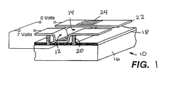
Figure 1 of the drawings shows an example of a part of a VisibleSpectrum Modulator Array 10 which may be fabricated in accordance with techniques described herein. Referring toFigure 1 , an antenna array is fabricated on one-half of a microfabricated interferometric cavity which transmits and reflects certain portions of incident electromagnetic radiation depending on (a) the dimensions of the cavity itself and (b) the frequency of response of dielectric mirrors in the cavities. InFigure 1 , thearray 10 is shown to include twocavities membrane 22. Each array element has anantenna array 24 formed on themembrane 22. The twostructures conductor 22/24 forms a flexible membrane, fabricated such that it is under tensile stress and thus parallel to the substrate, in an undriven state. - Because
layers 22 and 18 are parallel, radiation which enters any of the cavities from above or below the array can undergo multiple reflections within the cavity, resulting in optical interference. Depending on the dimensions of the antenna array, the interference will determine its reflective and/or transmissive characteristics. Changing one of the dimensions, in this case the cavity height (i.e. the spacing between the inner walls of layers 18, 22), will alter the optical characteristics. The change in height is achieved by applying a voltage across the two layers of the cavity, which due to electrostatic forces, causeslayer 22 to collapse.Cavity 12 is shown collapsed (7 volts applied), whilecavity 14 is shown uncollapsed (0 volts applied). - In fabricating the
array 10, it is desirable that insulating supports 20 are well defined in regions where contact is made betweeninsulating supports 20 andlayers 18, 22. The present invention is especially useful in manufacturing such a support.Figures 2 through 10 show various stages in the manufacture of a MEMS device having supports such as the supports 20. Referring toFigure 2 of the drawings,reference numeral 100 indicates asubstrate 100. Thesubstrate 100 may be of many different materials each being transparent to ultraviolet light. Examples of these materials include plastic, mylar, or quartz. The material must be able to support an optically smooth, though not necessarily flat, finish. A preferred material would likely be glass, which would be both transmissive and reflective operation in the visible range. - Various layers are deposited on
substrate 100 to define a stack. In particular, thesubstrate 100 is coated with asacrificial layer 102 using standard techniques such as a physical vapor deposition (PVD) method such as sputtering or e-beam evaporation. Other possible methods include chemical vapor deposition and molecular beam epitaxy. - In
Figure 2 , the sacrificial layer is a single layer. However, in other embodiments of theinvention layer 102 may be a stack of layers with an uppermost sacrificial layer. -
Figure 3 of the drawings shows a stage in the manufacture of the MEMS device wherein thesacrificial layer 102 has been patterned so as to define longitudinally spacedgrooves 104. A standard procedure is used to patternsacrificial layer 102 which includes exposinglayer 102 through an appropriate mask and developing to produce the pattern. - In
Figure 4 of the drawings, a photosensitive polymeric material in the form of a negative-acting-photosensitive material which could be a negative photoresist has been spun ontosacrificial layer 102 with a thickness that is larger than the total height of the film stack defined bylayers substrate 100 and developed using conventional techniques. Because thelongitudinal grooves 104 are the only means by which the negative-acting-photosensitive material is exposed, the negative-acting-photosensitive material over the stack is dissolved during a subsequent development process, leaving onlylongitudinal ridges 106 of negative-acting-photosensitive material disposed ingrooves 104. Thus, it will be appreciated that by first patterning thesacrificial layer 102 and then exposing the negative-acting-photosensitive material throughsubstrate 100 throughlongitudinal grooves 104 in thesacrificial layer 102, thesacrificial layer 102 acts as a photomask thereby allowing the negative-acting-photosensitive material to be lithographically patterned without the need for an additional masking step. InFigure 5 of the drawings, astructural layer 108 has been deposited on the stack and thesacrificial layer 102 has been removed, thus thelayer 108 is supported byridges 106. It will be appreciated that by using different photomasks it will be possible to fabricate support structures of any desired geometry. Thus instead of ridges, in other embodiments pillars or posts may be formed. Thelayer 108 is highly conductive and reflective and will typically contain aluminum and nickel. -
Figure 6 of the drawings shows a subsequent stage in the manufacture of the MEMS device wherein thelayer 108 is patterned into transversely extending strips.Figure 7 of the drawings shows the film stack with anoxide spacer layer 110 deposited onlayer 108.Figure 8 of the drawings shows a stage in the manufacture of the MEMS device in which theoxide spacer layer 110 has been patterned.Figure 9 of the drawings shows a stage in the manufacture of the MEMS device in which asealing film 112 is being applied with a pressure adhesive 114 over the entire structure to protect the structure from damage due to mechanical shock loading and to prevent particulates from interfering with the operation of the IMOD structures. Thesealing film 112 could be of a variety of materials such as thin metal films or polymeric films which have been coated with a metal or oxide film to provide hermeticity. Finally,Figure 10 shows the structure after it has been purged with XeF2 gas to remove the remains ofsacrificial layer 102. The edges of the structure are then sealed.
In other embodiments, instead ofoxide layer 110 another layer of negative-acting-photosensitive material may be spun overoxide layer 110 and exposed throughsubstrate 100 and using the techniques described above a further set of support structures may be formed. These support structures will provide support for other layers. It will be appreciated that the process may be repeated to build a MEMS structure having multiple layers or "floors" stacked one on top of the other wherein the floors are vertically spaced by support structures fabricated in accordance with the above techniques. One advantage of the present invention is that it provides a microfabrication technique which allows a mechanical support between two layers in an MEMS device to be precisely defined. This allows a clean, well-defined mechanical contact between the support and other structures within the MEMS device.
Further, the present invention uses a patterned layer on a substrate as a photomask to pattern another layer, thereby saving on a masking step.
The specification and drawings are to be regarded in an illustrative sense rather than in a restrictive sense.
Claims (15)
- A microfabrication process for fabricating a microelectromechanical systems device, comprising:depositing one or a stack of layers on a substrate (100), the substrate permitting light to pass therethrough;patterning said one or a stack of layers;depositing a middle layer on said one or a stack of layers, wherein the middle layer comprises a negative-acting photosensitive material;patterning the middle layer using said one or the uppermost layer of said stack of layers as a photomask; anddepositing an upper layer (108) after patterning of the middle layer;characterised in that said one or the uppermost layer of said stack of layers is a sacrificial layer (102), such that the middle layer is patterned using said sacrificial layer as a photomask..
- A method as claimed in claim 1, wherein the substrate (100) comprises glass.
- A method as claimed in claim 1 or 2, further comprising patterning said upper layer (108).
- A method as claimed in claim 1, 2 or 3, wherein patterning said one or a stack of layers comprises forming longitudinally spaced grooves (104) therein.
- A method as claimed in claim 4, wherein patterning said middle layer comprises exposing said middle layer to light passed through the grooves (104) in the one or a stack of layers.
- A method as claimed in claim 5, further comprising developing said middle layer to form longitudinally spaced ridges (106) in the said middle layer disposed in the grooves (104) in said one or a stack of layers.
- A method as claimed in claim 6, wherein said upper layer (108) is patterned to define transversely extending strips which are supported by the longitudinally spaced ridges (106) in the said middle layer.
- A method as claimed in any preceding claim, wherein said upper layer (108) comprises nickel and aluminum.
- A method as claimed in claim 1, wherein:patterning said one or a stack of layers comprises forming at least one aperture (104) therethrough through which said substrate (100) is exposed;the middle layer comprises a photosensitive layer; andpatterning said photosensitive layer comprises passing light through said at least one aperture (104) to expose said photosensitive layer.
- A method as claimed in claim 9, wherein the exposed portion of the middle layer forms supports for the upper layer (108).
- A method as claimed in any preceding claim, wherein said light comprises ultraviolet light
- A method as claimed in any preceding claim, wherein said upper layer (108) comprises a structural layer (108).
- A method as claimed in claim 12, wherein the steps of claim 1 are repeated at least once, and wherein each additional one or a stack of layers is deposited over an underlying structural layer (108).
- A method as claimed in any preceding claim, further comprising removing said sacrificial layer (102) after deposition of the upper layer (108).
- A method as claimed in any preceding claim, wherein depositing a middle layer comprises a spin-on process
Priority Applications (1)
| Application Number | Priority Date | Filing Date | Title |
|---|---|---|---|
| EP08022358A EP2042466A3 (en) | 2002-02-12 | 2002-04-29 | A method for fabricating a structure for a microelectromechanical systems (MEMS) device |
Applications Claiming Priority (3)
| Application Number | Priority Date | Filing Date | Title |
|---|---|---|---|
| US74562 | 2002-02-12 | ||
| US10/074,562 US6794119B2 (en) | 2002-02-12 | 2002-02-12 | Method for fabricating a structure for a microelectromechanical systems (MEMS) device |
| PCT/US2002/013442 WO2003069413A1 (en) | 2002-02-12 | 2002-04-29 | A method for fabricating a structure for a microelectromechanical systems (mems) device |
Related Child Applications (1)
| Application Number | Title | Priority Date | Filing Date |
|---|---|---|---|
| EP08022358A Division EP2042466A3 (en) | 2002-02-12 | 2002-04-29 | A method for fabricating a structure for a microelectromechanical systems (MEMS) device |
Publications (3)
| Publication Number | Publication Date |
|---|---|
| EP1485758A1 EP1485758A1 (en) | 2004-12-15 |
| EP1485758A4 EP1485758A4 (en) | 2006-09-13 |
| EP1485758B1 true EP1485758B1 (en) | 2008-12-31 |
Family
ID=27659905
Family Applications (2)
| Application Number | Title | Priority Date | Filing Date |
|---|---|---|---|
| EP08022358A Withdrawn EP2042466A3 (en) | 2002-02-12 | 2002-04-29 | A method for fabricating a structure for a microelectromechanical systems (MEMS) device |
| EP02725847A Expired - Lifetime EP1485758B1 (en) | 2002-02-12 | 2002-04-29 | A method for fabricating a structure for a microelectromechanical systems (mems) device |
Family Applications Before (1)
| Application Number | Title | Priority Date | Filing Date |
|---|---|---|---|
| EP08022358A Withdrawn EP2042466A3 (en) | 2002-02-12 | 2002-04-29 | A method for fabricating a structure for a microelectromechanical systems (MEMS) device |
Country Status (9)
| Country | Link |
|---|---|
| US (3) | US6794119B2 (en) |
| EP (2) | EP2042466A3 (en) |
| JP (2) | JP4633362B2 (en) |
| KR (1) | KR100947813B1 (en) |
| CN (2) | CN101284643B (en) |
| AT (1) | ATE419561T1 (en) |
| AU (1) | AU2002256386A1 (en) |
| DE (1) | DE60230680D1 (en) |
| WO (1) | WO2003069413A1 (en) |
Families Citing this family (309)
| Publication number | Priority date | Publication date | Assignee | Title |
|---|---|---|---|---|
| US5877897A (en) | 1993-02-26 | 1999-03-02 | Donnelly Corporation | Automatic rearview mirror, vehicle lighting control and vehicle interior monitoring system using a photosensor array |
| US6822563B2 (en) | 1997-09-22 | 2004-11-23 | Donnelly Corporation | Vehicle imaging system with accessory control |
| US6674562B1 (en) | 1994-05-05 | 2004-01-06 | Iridigm Display Corporation | Interferometric modulation of radiation |
| US8014059B2 (en) | 1994-05-05 | 2011-09-06 | Qualcomm Mems Technologies, Inc. | System and method for charge control in a MEMS device |
| US7550794B2 (en) | 2002-09-20 | 2009-06-23 | Idc, Llc | Micromechanical systems device comprising a displaceable electrode and a charge-trapping layer |
| US7297471B1 (en) | 2003-04-15 | 2007-11-20 | Idc, Llc | Method for manufacturing an array of interferometric modulators |
| US6891563B2 (en) | 1996-05-22 | 2005-05-10 | Donnelly Corporation | Vehicular vision system |
| US7907319B2 (en) | 1995-11-06 | 2011-03-15 | Qualcomm Mems Technologies, Inc. | Method and device for modulating light with optical compensation |
| US7655894B2 (en) | 1996-03-25 | 2010-02-02 | Donnelly Corporation | Vehicular image sensing system |
| US8928967B2 (en) | 1998-04-08 | 2015-01-06 | Qualcomm Mems Technologies, Inc. | Method and device for modulating light |
| WO1999052006A2 (en) | 1998-04-08 | 1999-10-14 | Etalon, Inc. | Interferometric modulation of radiation |
| US8023724B2 (en) * | 1999-07-22 | 2011-09-20 | Photon-X, Inc. | Apparatus and method of information extraction from electromagnetic energy based upon multi-characteristic spatial geometry processing |
| WO2003007049A1 (en) | 1999-10-05 | 2003-01-23 | Iridigm Display Corporation | Photonic mems and structures |
| US7167796B2 (en) * | 2000-03-09 | 2007-01-23 | Donnelly Corporation | Vehicle navigation system for use with a telematics system |
| US7697027B2 (en) | 2001-07-31 | 2010-04-13 | Donnelly Corporation | Vehicular video system |
| US6882287B2 (en) | 2001-07-31 | 2005-04-19 | Donnelly Corporation | Automotive lane change aid |
| US6794119B2 (en) * | 2002-02-12 | 2004-09-21 | Iridigm Display Corporation | Method for fabricating a structure for a microelectromechanical systems (MEMS) device |
| US6574033B1 (en) | 2002-02-27 | 2003-06-03 | Iridigm Display Corporation | Microelectromechanical systems device and method for fabricating same |
| EP1504276B1 (en) | 2002-05-03 | 2012-08-08 | Donnelly Corporation | Object detection system for vehicle |
| US7781850B2 (en) | 2002-09-20 | 2010-08-24 | Qualcomm Mems Technologies, Inc. | Controlling electromechanical behavior of structures within a microelectromechanical systems device |
| TWI289708B (en) | 2002-12-25 | 2007-11-11 | Qualcomm Mems Technologies Inc | Optical interference type color display |
| TW200413810A (en) * | 2003-01-29 | 2004-08-01 | Prime View Int Co Ltd | Light interference display panel and its manufacturing method |
| US7417782B2 (en) | 2005-02-23 | 2008-08-26 | Pixtronix, Incorporated | Methods and apparatus for spatial light modulation |
| TW570896B (en) | 2003-05-26 | 2004-01-11 | Prime View Int Co Ltd | A method for fabricating an interference display cell |
| US7221495B2 (en) * | 2003-06-24 | 2007-05-22 | Idc Llc | Thin film precursor stack for MEMS manufacturing |
| TWI251712B (en) * | 2003-08-15 | 2006-03-21 | Prime View Int Corp Ltd | Interference display plate |
| TW593127B (en) * | 2003-08-18 | 2004-06-21 | Prime View Int Co Ltd | Interference display plate and manufacturing method thereof |
| TW593126B (en) * | 2003-09-30 | 2004-06-21 | Prime View Int Co Ltd | A structure of a micro electro mechanical system and manufacturing the same |
| US7308341B2 (en) | 2003-10-14 | 2007-12-11 | Donnelly Corporation | Vehicle communication system |
| US7012726B1 (en) * | 2003-11-03 | 2006-03-14 | Idc, Llc | MEMS devices with unreleased thin film components |
| US7161728B2 (en) * | 2003-12-09 | 2007-01-09 | Idc, Llc | Area array modulation and lead reduction in interferometric modulators |
| US7368228B2 (en) * | 2003-12-19 | 2008-05-06 | Palo Alto Research Center Incorporated | Multilayer MEMS device and method of making same |
| US7342705B2 (en) | 2004-02-03 | 2008-03-11 | Idc, Llc | Spatial light modulator with integrated optical compensation structure |
| US7119945B2 (en) * | 2004-03-03 | 2006-10-10 | Idc, Llc | Altering temporal response of microelectromechanical elements |
| US7706050B2 (en) | 2004-03-05 | 2010-04-27 | Qualcomm Mems Technologies, Inc. | Integrated modulator illumination |
| US7855824B2 (en) | 2004-03-06 | 2010-12-21 | Qualcomm Mems Technologies, Inc. | Method and system for color optimization in a display |
| US7526103B2 (en) | 2004-04-15 | 2009-04-28 | Donnelly Corporation | Imaging system for vehicle |
| US7476327B2 (en) | 2004-05-04 | 2009-01-13 | Idc, Llc | Method of manufacture for microelectromechanical devices |
| US7164520B2 (en) | 2004-05-12 | 2007-01-16 | Idc, Llc | Packaging for an interferometric modulator |
| KR101255691B1 (en) | 2004-07-29 | 2013-04-17 | 퀄컴 엠이엠에스 테크놀로지스, 인크. | System and method for micro-electromechanical operating of an interferometric modulator |
| US7499208B2 (en) * | 2004-08-27 | 2009-03-03 | Udc, Llc | Current mode display driver circuit realization feature |
| US7889163B2 (en) | 2004-08-27 | 2011-02-15 | Qualcomm Mems Technologies, Inc. | Drive method for MEMS devices |
| US7944599B2 (en) | 2004-09-27 | 2011-05-17 | Qualcomm Mems Technologies, Inc. | Electromechanical device with optical function separated from mechanical and electrical function |
| US7532195B2 (en) | 2004-09-27 | 2009-05-12 | Idc, Llc | Method and system for reducing power consumption in a display |
| US7130104B2 (en) | 2004-09-27 | 2006-10-31 | Idc, Llc | Methods and devices for inhibiting tilting of a mirror in an interferometric modulator |
| US20060076634A1 (en) | 2004-09-27 | 2006-04-13 | Lauren Palmateer | Method and system for packaging MEMS devices with incorporated getter |
| US8878825B2 (en) | 2004-09-27 | 2014-11-04 | Qualcomm Mems Technologies, Inc. | System and method for providing a variable refresh rate of an interferometric modulator display |
| US8310441B2 (en) | 2004-09-27 | 2012-11-13 | Qualcomm Mems Technologies, Inc. | Method and system for writing data to MEMS display elements |
| US7920135B2 (en) | 2004-09-27 | 2011-04-05 | Qualcomm Mems Technologies, Inc. | Method and system for driving a bi-stable display |
| US8124434B2 (en) | 2004-09-27 | 2012-02-28 | Qualcomm Mems Technologies, Inc. | Method and system for packaging a display |
| US7446926B2 (en) | 2004-09-27 | 2008-11-04 | Idc, Llc | System and method of providing a regenerating protective coating in a MEMS device |
| US7417783B2 (en) * | 2004-09-27 | 2008-08-26 | Idc, Llc | Mirror and mirror layer for optical modulator and method |
| US7813026B2 (en) | 2004-09-27 | 2010-10-12 | Qualcomm Mems Technologies, Inc. | System and method of reducing color shift in a display |
| US7184202B2 (en) * | 2004-09-27 | 2007-02-27 | Idc, Llc | Method and system for packaging a MEMS device |
| US7710636B2 (en) | 2004-09-27 | 2010-05-04 | Qualcomm Mems Technologies, Inc. | Systems and methods using interferometric optical modulators and diffusers |
| US7612932B2 (en) | 2004-09-27 | 2009-11-03 | Idc, Llc | Microelectromechanical device with optical function separated from mechanical and electrical function |
| US7916103B2 (en) | 2004-09-27 | 2011-03-29 | Qualcomm Mems Technologies, Inc. | System and method for display device with end-of-life phenomena |
| US7679627B2 (en) | 2004-09-27 | 2010-03-16 | Qualcomm Mems Technologies, Inc. | Controller and driver features for bi-stable display |
| US7304784B2 (en) | 2004-09-27 | 2007-12-04 | Idc, Llc | Reflective display device having viewable display on both sides |
| US7653371B2 (en) | 2004-09-27 | 2010-01-26 | Qualcomm Mems Technologies, Inc. | Selectable capacitance circuit |
| US8008736B2 (en) | 2004-09-27 | 2011-08-30 | Qualcomm Mems Technologies, Inc. | Analog interferometric modulator device |
| US7561323B2 (en) | 2004-09-27 | 2009-07-14 | Idc, Llc | Optical films for directing light towards active areas of displays |
| US7327510B2 (en) | 2004-09-27 | 2008-02-05 | Idc, Llc | Process for modifying offset voltage characteristics of an interferometric modulator |
| US7843410B2 (en) | 2004-09-27 | 2010-11-30 | Qualcomm Mems Technologies, Inc. | Method and device for electrically programmable display |
| US20060065622A1 (en) * | 2004-09-27 | 2006-03-30 | Floyd Philip D | Method and system for xenon fluoride etching with enhanced efficiency |
| US7551246B2 (en) * | 2004-09-27 | 2009-06-23 | Idc, Llc. | System and method for display device with integrated desiccant |
| US7573547B2 (en) * | 2004-09-27 | 2009-08-11 | Idc, Llc | System and method for protecting micro-structure of display array using spacers in gap within display device |
| US7420725B2 (en) | 2004-09-27 | 2008-09-02 | Idc, Llc | Device having a conductive light absorbing mask and method for fabricating same |
| US7807488B2 (en) | 2004-09-27 | 2010-10-05 | Qualcomm Mems Technologies, Inc. | Display element having filter material diffused in a substrate of the display element |
| US7701631B2 (en) | 2004-09-27 | 2010-04-20 | Qualcomm Mems Technologies, Inc. | Device having patterned spacers for backplates and method of making the same |
| US7349141B2 (en) * | 2004-09-27 | 2008-03-25 | Idc, Llc | Method and post structures for interferometric modulation |
| US7710629B2 (en) | 2004-09-27 | 2010-05-04 | Qualcomm Mems Technologies, Inc. | System and method for display device with reinforcing substance |
| US7508571B2 (en) | 2004-09-27 | 2009-03-24 | Idc, Llc | Optical films for controlling angular characteristics of displays |
| US7630123B2 (en) | 2004-09-27 | 2009-12-08 | Qualcomm Mems Technologies, Inc. | Method and device for compensating for color shift as a function of angle of view |
| US7684104B2 (en) | 2004-09-27 | 2010-03-23 | Idc, Llc | MEMS using filler material and method |
| US7724993B2 (en) | 2004-09-27 | 2010-05-25 | Qualcomm Mems Technologies, Inc. | MEMS switches with deforming membranes |
| US7719500B2 (en) | 2004-09-27 | 2010-05-18 | Qualcomm Mems Technologies, Inc. | Reflective display pixels arranged in non-rectangular arrays |
| US7630119B2 (en) | 2004-09-27 | 2009-12-08 | Qualcomm Mems Technologies, Inc. | Apparatus and method for reducing slippage between structures in an interferometric modulator |
| US7136213B2 (en) | 2004-09-27 | 2006-11-14 | Idc, Llc | Interferometric modulators having charge persistence |
| US7583429B2 (en) | 2004-09-27 | 2009-09-01 | Idc, Llc | Ornamental display device |
| US7527995B2 (en) | 2004-09-27 | 2009-05-05 | Qualcomm Mems Technologies, Inc. | Method of making prestructure for MEMS systems |
| US7668415B2 (en) * | 2004-09-27 | 2010-02-23 | Qualcomm Mems Technologies, Inc. | Method and device for providing electronic circuitry on a backplate |
| US7675669B2 (en) * | 2004-09-27 | 2010-03-09 | Qualcomm Mems Technologies, Inc. | Method and system for driving interferometric modulators |
| US7355780B2 (en) | 2004-09-27 | 2008-04-08 | Idc, Llc | System and method of illuminating interferometric modulators using backlighting |
| US7424198B2 (en) | 2004-09-27 | 2008-09-09 | Idc, Llc | Method and device for packaging a substrate |
| US7369296B2 (en) | 2004-09-27 | 2008-05-06 | Idc, Llc | Device and method for modifying actuation voltage thresholds of a deformable membrane in an interferometric modulator |
| US7936497B2 (en) | 2004-09-27 | 2011-05-03 | Qualcomm Mems Technologies, Inc. | MEMS device having deformable membrane characterized by mechanical persistence |
| US7289259B2 (en) | 2004-09-27 | 2007-10-30 | Idc, Llc | Conductive bus structure for interferometric modulator array |
| US7692839B2 (en) | 2004-09-27 | 2010-04-06 | Qualcomm Mems Technologies, Inc. | System and method of providing MEMS device with anti-stiction coating |
| US7373026B2 (en) | 2004-09-27 | 2008-05-13 | Idc, Llc | MEMS device fabricated on a pre-patterned substrate |
| US7553684B2 (en) * | 2004-09-27 | 2009-06-30 | Idc, Llc | Method of fabricating interferometric devices using lift-off processing techniques |
| US7808703B2 (en) | 2004-09-27 | 2010-10-05 | Qualcomm Mems Technologies, Inc. | System and method for implementation of interferometric modulator displays |
| US7405924B2 (en) * | 2004-09-27 | 2008-07-29 | Idc, Llc | System and method for protecting microelectromechanical systems array using structurally reinforced back-plate |
| US7302157B2 (en) | 2004-09-27 | 2007-11-27 | Idc, Llc | System and method for multi-level brightness in interferometric modulation |
| US7750886B2 (en) | 2004-09-27 | 2010-07-06 | Qualcomm Mems Technologies, Inc. | Methods and devices for lighting displays |
| US7372613B2 (en) | 2004-09-27 | 2008-05-13 | Idc, Llc | Method and device for multistate interferometric light modulation |
| US7893919B2 (en) | 2004-09-27 | 2011-02-22 | Qualcomm Mems Technologies, Inc. | Display region architectures |
| US7321456B2 (en) | 2004-09-27 | 2008-01-22 | Idc, Llc | Method and device for corner interferometric modulation |
| US7564612B2 (en) | 2004-09-27 | 2009-07-21 | Idc, Llc | Photonic MEMS and structures |
| US7881496B2 (en) | 2004-09-30 | 2011-02-01 | Donnelly Corporation | Vision system for vehicle |
| US7720580B2 (en) | 2004-12-23 | 2010-05-18 | Donnelly Corporation | Object detection system for vehicle |
| TWI293401B (en) * | 2004-12-30 | 2008-02-11 | Au Optronics Corp | Microelectrooptomechanical device and fabricating method thereof |
| TWI249191B (en) * | 2004-12-31 | 2006-02-11 | Au Optronics Corp | Method for fabricating a microelectromechanical optical display device |
| US7463406B2 (en) * | 2004-12-31 | 2008-12-09 | Au Optronics Corp. | Method for fabricating microelectromechanical optical display devices |
| CN100360982C (en) * | 2005-01-13 | 2008-01-09 | 友达光电股份有限公司 | Microelectromechanical optical display subass embly |
| CN1296271C (en) * | 2005-01-26 | 2007-01-24 | 友达光电股份有限公司 | Manufacturing method of micro-mechanoelectric optical display unit |
| US7746529B2 (en) | 2005-02-23 | 2010-06-29 | Pixtronix, Inc. | MEMS display apparatus |
| US9082353B2 (en) | 2010-01-05 | 2015-07-14 | Pixtronix, Inc. | Circuits for controlling display apparatus |
| US9261694B2 (en) | 2005-02-23 | 2016-02-16 | Pixtronix, Inc. | Display apparatus and methods for manufacture thereof |
| US7999994B2 (en) | 2005-02-23 | 2011-08-16 | Pixtronix, Inc. | Display apparatus and methods for manufacture thereof |
| US7755582B2 (en) | 2005-02-23 | 2010-07-13 | Pixtronix, Incorporated | Display methods and apparatus |
| US20070205969A1 (en) | 2005-02-23 | 2007-09-06 | Pixtronix, Incorporated | Direct-view MEMS display devices and methods for generating images thereon |
| US7742016B2 (en) | 2005-02-23 | 2010-06-22 | Pixtronix, Incorporated | Display methods and apparatus |
| US8482496B2 (en) | 2006-01-06 | 2013-07-09 | Pixtronix, Inc. | Circuits for controlling MEMS display apparatus on a transparent substrate |
| US8519945B2 (en) | 2006-01-06 | 2013-08-27 | Pixtronix, Inc. | Circuits for controlling display apparatus |
| US9229222B2 (en) | 2005-02-23 | 2016-01-05 | Pixtronix, Inc. | Alignment methods in fluid-filled MEMS displays |
| US7675665B2 (en) | 2005-02-23 | 2010-03-09 | Pixtronix, Incorporated | Methods and apparatus for actuating displays |
| US8310442B2 (en) | 2005-02-23 | 2012-11-13 | Pixtronix, Inc. | Circuits for controlling display apparatus |
| US8159428B2 (en) | 2005-02-23 | 2012-04-17 | Pixtronix, Inc. | Display methods and apparatus |
| US9158106B2 (en) | 2005-02-23 | 2015-10-13 | Pixtronix, Inc. | Display methods and apparatus |
| KR20080027236A (en) | 2005-05-05 | 2008-03-26 | 콸콤 인코포레이티드 | Dynamic driver ic and display panel configuration |
| US7948457B2 (en) | 2005-05-05 | 2011-05-24 | Qualcomm Mems Technologies, Inc. | Systems and methods of actuating MEMS display elements |
| US7920136B2 (en) | 2005-05-05 | 2011-04-05 | Qualcomm Mems Technologies, Inc. | System and method of driving a MEMS display device |
| US7884989B2 (en) | 2005-05-27 | 2011-02-08 | Qualcomm Mems Technologies, Inc. | White interferometric modulators and methods for forming the same |
| CN101228091A (en) | 2005-07-22 | 2008-07-23 | 高通股份有限公司 | Support structure for MEMS device and methods thereof |
| JP2009503564A (en) * | 2005-07-22 | 2009-01-29 | クアルコム,インコーポレイテッド | Support structure for MEMS device and method thereof |
| EP1910218A1 (en) * | 2005-07-22 | 2008-04-16 | Qualcomm Mems Technologies, Inc. | Mems devices having support structures and methods of fabricating the same |
| EP2495212A3 (en) | 2005-07-22 | 2012-10-31 | QUALCOMM MEMS Technologies, Inc. | Mems devices having support structures and methods of fabricating the same |
| US7630114B2 (en) * | 2005-10-28 | 2009-12-08 | Idc, Llc | Diffusion barrier layer for MEMS devices |
| KR100744543B1 (en) * | 2005-12-08 | 2007-08-01 | 한국전자통신연구원 | Micro-electro mechanical systems switch and method of fabricating the same switch |
| US8391630B2 (en) | 2005-12-22 | 2013-03-05 | Qualcomm Mems Technologies, Inc. | System and method for power reduction when decompressing video streams for interferometric modulator displays |
| US7795061B2 (en) | 2005-12-29 | 2010-09-14 | Qualcomm Mems Technologies, Inc. | Method of creating MEMS device cavities by a non-etching process |
| US7916980B2 (en) * | 2006-01-13 | 2011-03-29 | Qualcomm Mems Technologies, Inc. | Interconnect structure for MEMS device |
| US7382515B2 (en) | 2006-01-18 | 2008-06-03 | Qualcomm Mems Technologies, Inc. | Silicon-rich silicon nitrides as etch stops in MEMS manufacture |
| US7652814B2 (en) | 2006-01-27 | 2010-01-26 | Qualcomm Mems Technologies, Inc. | MEMS device with integrated optical element |
| US8194056B2 (en) | 2006-02-09 | 2012-06-05 | Qualcomm Mems Technologies Inc. | Method and system for writing data to MEMS display elements |
| US7603001B2 (en) * | 2006-02-17 | 2009-10-13 | Qualcomm Mems Technologies, Inc. | Method and apparatus for providing back-lighting in an interferometric modulator display device |
| US8526096B2 (en) | 2006-02-23 | 2013-09-03 | Pixtronix, Inc. | Mechanical light modulators with stressed beams |
| US7450295B2 (en) | 2006-03-02 | 2008-11-11 | Qualcomm Mems Technologies, Inc. | Methods for producing MEMS with protective coatings using multi-component sacrificial layers |
| US7643203B2 (en) | 2006-04-10 | 2010-01-05 | Qualcomm Mems Technologies, Inc. | Interferometric optical display system with broadband characteristics |
| WO2007120887A2 (en) * | 2006-04-13 | 2007-10-25 | Qualcomm Mems Technologies, Inc | Packaging a mems device using a frame |
| US7903047B2 (en) | 2006-04-17 | 2011-03-08 | Qualcomm Mems Technologies, Inc. | Mode indicator for interferometric modulator displays |
| US7527996B2 (en) * | 2006-04-19 | 2009-05-05 | Qualcomm Mems Technologies, Inc. | Non-planar surface structures and process for microelectromechanical systems |
| US7711239B2 (en) | 2006-04-19 | 2010-05-04 | Qualcomm Mems Technologies, Inc. | Microelectromechanical device and method utilizing nanoparticles |
| US20070249078A1 (en) * | 2006-04-19 | 2007-10-25 | Ming-Hau Tung | Non-planar surface structures and process for microelectromechanical systems |
| US7623287B2 (en) * | 2006-04-19 | 2009-11-24 | Qualcomm Mems Technologies, Inc. | Non-planar surface structures and process for microelectromechanical systems |
| US8049713B2 (en) | 2006-04-24 | 2011-11-01 | Qualcomm Mems Technologies, Inc. | Power consumption optimized display update |
| US7369292B2 (en) | 2006-05-03 | 2008-05-06 | Qualcomm Mems Technologies, Inc. | Electrode and interconnect materials for MEMS devices |
| US7321457B2 (en) | 2006-06-01 | 2008-01-22 | Qualcomm Incorporated | Process and structure for fabrication of MEMS device having isolated edge posts |
| US7649671B2 (en) | 2006-06-01 | 2010-01-19 | Qualcomm Mems Technologies, Inc. | Analog interferometric modulator device with electrostatic actuation and release |
| US7876489B2 (en) | 2006-06-05 | 2011-01-25 | Pixtronix, Inc. | Display apparatus with optical cavities |
| US7702192B2 (en) | 2006-06-21 | 2010-04-20 | Qualcomm Mems Technologies, Inc. | Systems and methods for driving MEMS display |
| US7766498B2 (en) | 2006-06-21 | 2010-08-03 | Qualcomm Mems Technologies, Inc. | Linear solid state illuminator |
| US7835061B2 (en) | 2006-06-28 | 2010-11-16 | Qualcomm Mems Technologies, Inc. | Support structures for free-standing electromechanical devices |
| US7777715B2 (en) | 2006-06-29 | 2010-08-17 | Qualcomm Mems Technologies, Inc. | Passive circuits for de-multiplexing display inputs |
| US7527998B2 (en) | 2006-06-30 | 2009-05-05 | Qualcomm Mems Technologies, Inc. | Method of manufacturing MEMS devices providing air gap control |
| JP4327183B2 (en) * | 2006-07-31 | 2009-09-09 | 株式会社日立製作所 | High pressure fuel pump control device for internal combustion engine |
| US7763546B2 (en) | 2006-08-02 | 2010-07-27 | Qualcomm Mems Technologies, Inc. | Methods for reducing surface charges during the manufacture of microelectromechanical systems devices |
| US7972045B2 (en) | 2006-08-11 | 2011-07-05 | Donnelly Corporation | Automatic headlamp control system |
| US7845841B2 (en) | 2006-08-28 | 2010-12-07 | Qualcomm Mems Technologies, Inc. | Angle sweeping holographic illuminator |
| WO2008045207A2 (en) | 2006-10-06 | 2008-04-17 | Qualcomm Mems Technologies, Inc. | Light guide |
| EP2366942A1 (en) | 2006-10-06 | 2011-09-21 | Qualcomm Mems Technologies, Inc. | Optical loss layer integrated in an illumination apparatus of a display |
| US8107155B2 (en) | 2006-10-06 | 2012-01-31 | Qualcomm Mems Technologies, Inc. | System and method for reducing visual artifacts in displays |
| US7855827B2 (en) | 2006-10-06 | 2010-12-21 | Qualcomm Mems Technologies, Inc. | Internal optical isolation structure for integrated front or back lighting |
| EP1946162A2 (en) | 2006-10-10 | 2008-07-23 | Qualcomm Mems Technologies, Inc | Display device with diffractive optics |
| US7629197B2 (en) | 2006-10-18 | 2009-12-08 | Qualcomm Mems Technologies, Inc. | Spatial light modulator |
| US7545552B2 (en) * | 2006-10-19 | 2009-06-09 | Qualcomm Mems Technologies, Inc. | Sacrificial spacer process and resultant structure for MEMS support structure |
| WO2008051362A1 (en) | 2006-10-20 | 2008-05-02 | Pixtronix, Inc. | Light guides and backlight systems incorporating light redirectors at varying densities |
| US7864395B2 (en) | 2006-10-27 | 2011-01-04 | Qualcomm Mems Technologies, Inc. | Light guide including optical scattering elements and a method of manufacture |
| US7706042B2 (en) | 2006-12-20 | 2010-04-27 | Qualcomm Mems Technologies, Inc. | MEMS device and interconnects for same |
| US9176318B2 (en) | 2007-05-18 | 2015-11-03 | Pixtronix, Inc. | Methods for manufacturing fluid-filled MEMS displays |
| US7852546B2 (en) | 2007-10-19 | 2010-12-14 | Pixtronix, Inc. | Spacers for maintaining display apparatus alignment |
| EP3624086A1 (en) | 2007-01-25 | 2020-03-18 | Magna Electronics Inc. | Radar sensing system for vehicle |
| US7777954B2 (en) | 2007-01-30 | 2010-08-17 | Qualcomm Mems Technologies, Inc. | Systems and methods of providing a light guiding layer |
| US8115987B2 (en) | 2007-02-01 | 2012-02-14 | Qualcomm Mems Technologies, Inc. | Modulating the intensity of light from an interferometric reflector |
| US7733552B2 (en) | 2007-03-21 | 2010-06-08 | Qualcomm Mems Technologies, Inc | MEMS cavity-coating layers and methods |
| US7742220B2 (en) | 2007-03-28 | 2010-06-22 | Qualcomm Mems Technologies, Inc. | Microelectromechanical device and method utilizing conducting layers separated by stops |
| US7733439B2 (en) | 2007-04-30 | 2010-06-08 | Qualcomm Mems Technologies, Inc. | Dual film light guide for illuminating displays |
| US7643202B2 (en) | 2007-05-09 | 2010-01-05 | Qualcomm Mems Technologies, Inc. | Microelectromechanical system having a dielectric movable membrane and a mirror |
| US7715085B2 (en) | 2007-05-09 | 2010-05-11 | Qualcomm Mems Technologies, Inc. | Electromechanical system having a dielectric movable membrane and a mirror |
| US7719752B2 (en) | 2007-05-11 | 2010-05-18 | Qualcomm Mems Technologies, Inc. | MEMS structures, methods of fabricating MEMS components on separate substrates and assembly of same |
| US7625825B2 (en) * | 2007-06-14 | 2009-12-01 | Qualcomm Mems Technologies, Inc. | Method of patterning mechanical layer for MEMS structures |
| US7643199B2 (en) * | 2007-06-19 | 2010-01-05 | Qualcomm Mems Technologies, Inc. | High aperture-ratio top-reflective AM-iMod displays |
| US7782517B2 (en) | 2007-06-21 | 2010-08-24 | Qualcomm Mems Technologies, Inc. | Infrared and dual mode displays |
| US7569488B2 (en) | 2007-06-22 | 2009-08-04 | Qualcomm Mems Technologies, Inc. | Methods of making a MEMS device by monitoring a process parameter |
| US7630121B2 (en) | 2007-07-02 | 2009-12-08 | Qualcomm Mems Technologies, Inc. | Electromechanical device with optical function separated from mechanical and electrical function |
| US8068268B2 (en) | 2007-07-03 | 2011-11-29 | Qualcomm Mems Technologies, Inc. | MEMS devices having improved uniformity and methods for making them |
| US7914187B2 (en) | 2007-07-12 | 2011-03-29 | Magna Electronics Inc. | Automatic lighting system with adaptive alignment function |
| WO2009015231A1 (en) * | 2007-07-25 | 2009-01-29 | Qualcomm Mems Technologies, Inc. | Mems display devices and methods of fabricating the same |
| WO2009018287A1 (en) | 2007-07-31 | 2009-02-05 | Qualcomm Mems Technologies, Inc. | Devices for enhancing colour shift of interferometric modulators |
| US8017898B2 (en) | 2007-08-17 | 2011-09-13 | Magna Electronics Inc. | Vehicular imaging system in an automatic headlamp control system |
| US8072402B2 (en) | 2007-08-29 | 2011-12-06 | Qualcomm Mems Technologies, Inc. | Interferometric optical modulator with broadband reflection characteristics |
| WO2009036176A1 (en) | 2007-09-11 | 2009-03-19 | Magna Electronics | Imaging system for vehicle |
| US7847999B2 (en) | 2007-09-14 | 2010-12-07 | Qualcomm Mems Technologies, Inc. | Interferometric modulator display devices |
| US7773286B2 (en) | 2007-09-14 | 2010-08-10 | Qualcomm Mems Technologies, Inc. | Periodic dimple array |
| JP5478493B2 (en) * | 2007-09-17 | 2014-04-23 | クォルコム・メムズ・テクノロジーズ・インコーポレーテッド | Translucent / semi-transmissive light emitting interference device |
| US8446470B2 (en) | 2007-10-04 | 2013-05-21 | Magna Electronics, Inc. | Combined RGB and IR imaging sensor |
| EP2212926A2 (en) | 2007-10-19 | 2010-08-04 | QUALCOMM MEMS Technologies, Inc. | Display with integrated photovoltaics |
| US8058549B2 (en) | 2007-10-19 | 2011-11-15 | Qualcomm Mems Technologies, Inc. | Photovoltaic devices with integrated color interferometric film stacks |
| US8054527B2 (en) | 2007-10-23 | 2011-11-08 | Qualcomm Mems Technologies, Inc. | Adjustably transmissive MEMS-based devices |
| US8941631B2 (en) | 2007-11-16 | 2015-01-27 | Qualcomm Mems Technologies, Inc. | Simultaneous light collection and illumination on an active display |
| US8068710B2 (en) | 2007-12-07 | 2011-11-29 | Qualcomm Mems Technologies, Inc. | Decoupled holographic film and diffuser |
| US7949213B2 (en) | 2007-12-07 | 2011-05-24 | Qualcomm Mems Technologies, Inc. | Light illumination of displays with front light guide and coupling elements |
| US7715079B2 (en) | 2007-12-07 | 2010-05-11 | Qualcomm Mems Technologies, Inc. | MEMS devices requiring no mechanical support |
| US7863079B2 (en) | 2008-02-05 | 2011-01-04 | Qualcomm Mems Technologies, Inc. | Methods of reducing CD loss in a microelectromechanical device |
| WO2009102733A2 (en) | 2008-02-12 | 2009-08-20 | Qualcomm Mems Technologies, Inc. | Integrated front light diffuser for reflective displays |
| WO2009102731A2 (en) | 2008-02-12 | 2009-08-20 | Qualcomm Mems Technologies, Inc. | Devices and methods for enhancing brightness of displays using angle conversion layers |
| US8164821B2 (en) | 2008-02-22 | 2012-04-24 | Qualcomm Mems Technologies, Inc. | Microelectromechanical device with thermal expansion balancing layer or stiffening layer |
| US7944604B2 (en) | 2008-03-07 | 2011-05-17 | Qualcomm Mems Technologies, Inc. | Interferometric modulator in transmission mode |
| JP5086149B2 (en) * | 2008-03-26 | 2012-11-28 | 日本電信電話株式会社 | Microstructure fabrication method |
| US7612933B2 (en) | 2008-03-27 | 2009-11-03 | Qualcomm Mems Technologies, Inc. | Microelectromechanical device with spacing layer |
| US7898723B2 (en) | 2008-04-02 | 2011-03-01 | Qualcomm Mems Technologies, Inc. | Microelectromechanical systems display element with photovoltaic structure |
| US7969638B2 (en) | 2008-04-10 | 2011-06-28 | Qualcomm Mems Technologies, Inc. | Device having thin black mask and method of fabricating the same |
| US8248560B2 (en) | 2008-04-18 | 2012-08-21 | Pixtronix, Inc. | Light guides and backlight systems incorporating prismatic structures and light redirectors |
| US8049951B2 (en) | 2008-04-15 | 2011-11-01 | Qualcomm Mems Technologies, Inc. | Light with bi-directional propagation |
| US7795056B2 (en) * | 2008-06-03 | 2010-09-14 | United Microelectronics Corp. | Semiconductor device and method of fabricating the same |
| US7851239B2 (en) | 2008-06-05 | 2010-12-14 | Qualcomm Mems Technologies, Inc. | Low temperature amorphous silicon sacrificial layer for controlled adhesion in MEMS devices |
| US7746539B2 (en) | 2008-06-25 | 2010-06-29 | Qualcomm Mems Technologies, Inc. | Method for packing a display device and the device obtained thereof |
| US7768690B2 (en) | 2008-06-25 | 2010-08-03 | Qualcomm Mems Technologies, Inc. | Backlight displays |
| US8023167B2 (en) | 2008-06-25 | 2011-09-20 | Qualcomm Mems Technologies, Inc. | Backlight displays |
| US7859740B2 (en) | 2008-07-11 | 2010-12-28 | Qualcomm Mems Technologies, Inc. | Stiction mitigation with integrated mech micro-cantilevers through vertical stress gradient control |
| US7782522B2 (en) | 2008-07-17 | 2010-08-24 | Qualcomm Mems Technologies, Inc. | Encapsulation methods for interferometric modulator and MEMS devices |
| US7855826B2 (en) | 2008-08-12 | 2010-12-21 | Qualcomm Mems Technologies, Inc. | Method and apparatus to reduce or eliminate stiction and image retention in interferometric modulator devices |
| US8358266B2 (en) | 2008-09-02 | 2013-01-22 | Qualcomm Mems Technologies, Inc. | Light turning device with prismatic light turning features |
| US7719754B2 (en) * | 2008-09-30 | 2010-05-18 | Qualcomm Mems Technologies, Inc. | Multi-thickness layers for MEMS and mask-saving sequence for same |
| US8169679B2 (en) | 2008-10-27 | 2012-05-01 | Pixtronix, Inc. | MEMS anchors |
| US8445306B2 (en) | 2008-12-24 | 2013-05-21 | International Business Machines Corporation | Hybrid MEMS RF switch and method of fabricating same |
| US8172417B2 (en) | 2009-03-06 | 2012-05-08 | Qualcomm Mems Technologies, Inc. | Shaped frontlight reflector for use with display |
| US9126525B2 (en) | 2009-02-27 | 2015-09-08 | Magna Electronics Inc. | Alert system for vehicle |
| US8270056B2 (en) | 2009-03-23 | 2012-09-18 | Qualcomm Mems Technologies, Inc. | Display device with openings between sub-pixels and method of making same |
| US8736590B2 (en) | 2009-03-27 | 2014-05-27 | Qualcomm Mems Technologies, Inc. | Low voltage driver scheme for interferometric modulators |
| US7864403B2 (en) | 2009-03-27 | 2011-01-04 | Qualcomm Mems Technologies, Inc. | Post-release adjustment of interferometric modulator reflectivity |
| US8604898B2 (en) | 2009-04-20 | 2013-12-10 | International Business Machines Corporation | Vertical integrated circuit switches, design structure and methods of fabricating same |
| US8376595B2 (en) | 2009-05-15 | 2013-02-19 | Magna Electronics, Inc. | Automatic headlamp control |
| US20100302218A1 (en) | 2009-05-29 | 2010-12-02 | Qualcomm Mems Technologies, Inc. | Illumination devices and methods of fabrication thereof |
| US8521106B2 (en) * | 2009-06-09 | 2013-08-27 | Broadcom Corporation | Method and system for a sub-harmonic transmitter utilizing a leaky wave antenna |
| CN102481874B (en) | 2009-07-27 | 2015-08-05 | 马格纳电子系统公司 | Parking assistance system |
| US9495876B2 (en) | 2009-07-27 | 2016-11-15 | Magna Electronics Inc. | Vehicular camera with on-board microcontroller |
| EP2473871B1 (en) | 2009-09-01 | 2015-03-11 | Magna Mirrors Of America, Inc. | Imaging and display system for vehicle |
| US8270062B2 (en) | 2009-09-17 | 2012-09-18 | Qualcomm Mems Technologies, Inc. | Display device with at least one movable stop element |
| US8488228B2 (en) | 2009-09-28 | 2013-07-16 | Qualcomm Mems Technologies, Inc. | Interferometric display with interferometric reflector |
| US8379392B2 (en) | 2009-10-23 | 2013-02-19 | Qualcomm Mems Technologies, Inc. | Light-based sealing and device packaging |
| US8711361B2 (en) * | 2009-11-05 | 2014-04-29 | Qualcomm, Incorporated | Methods and devices for detecting and measuring environmental conditions in high performance device packages |
| JP2013519122A (en) | 2010-02-02 | 2013-05-23 | ピクストロニックス・インコーポレーテッド | Circuit for controlling a display device |
| KR20120132680A (en) | 2010-02-02 | 2012-12-07 | 픽스트로닉스 인코포레이티드 | Methods for manufacturing cold seal fluid-filled display apparatus |
| US8890955B2 (en) | 2010-02-10 | 2014-11-18 | Magna Mirrors Of America, Inc. | Adaptable wireless vehicle vision system based on wireless communication error |
| US8730218B2 (en) * | 2010-02-12 | 2014-05-20 | Blackberry Limited | Ambient light-compensated reflective display devices and methods related thereto |
| CN102834761A (en) | 2010-04-09 | 2012-12-19 | 高通Mems科技公司 | Mechanical layer and methods of forming the same |
| KR101821727B1 (en) | 2010-04-16 | 2018-01-24 | 플렉스 라이팅 투 엘엘씨 | Front illumination device comprising a film-based lightguide |
| US9110200B2 (en) | 2010-04-16 | 2015-08-18 | Flex Lighting Ii, Llc | Illumination device comprising a film-based lightguide |
| US8848294B2 (en) | 2010-05-20 | 2014-09-30 | Qualcomm Mems Technologies, Inc. | Method and structure capable of changing color saturation |
| US9117123B2 (en) | 2010-07-05 | 2015-08-25 | Magna Electronics Inc. | Vehicular rear view camera display system with lifecheck function |
| CN103109315A (en) | 2010-08-17 | 2013-05-15 | 高通Mems科技公司 | Actuation and calibration of a charge neutral electrode in an interferometric display device |
| US9057872B2 (en) | 2010-08-31 | 2015-06-16 | Qualcomm Mems Technologies, Inc. | Dielectric enhanced mirror for IMOD display |
| WO2012068331A1 (en) | 2010-11-19 | 2012-05-24 | Magna Electronics Inc. | Lane keeping system and lane centering system |
| WO2012075250A1 (en) | 2010-12-01 | 2012-06-07 | Magna Electronics Inc. | System and method of establishing a multi-camera image using pixel remapping |
| US8902484B2 (en) | 2010-12-15 | 2014-12-02 | Qualcomm Mems Technologies, Inc. | Holographic brightness enhancement film |
| US9264672B2 (en) | 2010-12-22 | 2016-02-16 | Magna Mirrors Of America, Inc. | Vision display system for vehicle |
| US9085261B2 (en) | 2011-01-26 | 2015-07-21 | Magna Electronics Inc. | Rear vision system with trailer angle detection |
| US9134527B2 (en) | 2011-04-04 | 2015-09-15 | Qualcomm Mems Technologies, Inc. | Pixel via and methods of forming the same |
| US8963159B2 (en) | 2011-04-04 | 2015-02-24 | Qualcomm Mems Technologies, Inc. | Pixel via and methods of forming the same |
| US9194943B2 (en) | 2011-04-12 | 2015-11-24 | Magna Electronics Inc. | Step filter for estimating distance in a time-of-flight ranging system |
| US9547795B2 (en) | 2011-04-25 | 2017-01-17 | Magna Electronics Inc. | Image processing method for detecting objects using relative motion |
| WO2012145818A1 (en) | 2011-04-25 | 2012-11-01 | Magna International Inc. | Method and system for dynamically calibrating vehicular cameras |
| US8659816B2 (en) | 2011-04-25 | 2014-02-25 | Qualcomm Mems Technologies, Inc. | Mechanical layer and methods of making the same |
| WO2013016409A1 (en) | 2011-07-26 | 2013-01-31 | Magna Electronics Inc. | Vision system for vehicle |
| WO2013019707A1 (en) | 2011-08-01 | 2013-02-07 | Magna Electronics Inc. | Vehicle camera alignment system |
| US20140218535A1 (en) | 2011-09-21 | 2014-08-07 | Magna Electronics Inc. | Vehicle vision system using image data transmission and power supply via a coaxial cable |
| US9146898B2 (en) | 2011-10-27 | 2015-09-29 | Magna Electronics Inc. | Driver assist system with algorithm switching |
| US8736939B2 (en) | 2011-11-04 | 2014-05-27 | Qualcomm Mems Technologies, Inc. | Matching layer thin-films for an electromechanical systems reflective display device |
| WO2013074604A2 (en) | 2011-11-15 | 2013-05-23 | Magna Electronics, Inc. | Calibration system and method for vehicular surround vision system |
| WO2013081985A1 (en) | 2011-11-28 | 2013-06-06 | Magna Electronics, Inc. | Vision system for vehicle |
| US10457209B2 (en) | 2012-02-22 | 2019-10-29 | Magna Electronics Inc. | Vehicle vision system with multi-paned view |
| US8694224B2 (en) | 2012-03-01 | 2014-04-08 | Magna Electronics Inc. | Vehicle yaw rate correction |
| US9319637B2 (en) | 2012-03-27 | 2016-04-19 | Magna Electronics Inc. | Vehicle vision system with lens pollution detection |
| US10089537B2 (en) | 2012-05-18 | 2018-10-02 | Magna Electronics Inc. | Vehicle vision system with front and rear camera integration |
| US9340227B2 (en) | 2012-08-14 | 2016-05-17 | Magna Electronics Inc. | Vehicle lane keep assist system |
| DE102013217430A1 (en) | 2012-09-04 | 2014-03-06 | Magna Electronics, Inc. | Driver assistance system for a motor vehicle |
| US9558409B2 (en) | 2012-09-26 | 2017-01-31 | Magna Electronics Inc. | Vehicle vision system with trailer angle detection |
| US9446713B2 (en) | 2012-09-26 | 2016-09-20 | Magna Electronics Inc. | Trailer angle detection system |
| US9181086B1 (en) | 2012-10-01 | 2015-11-10 | The Research Foundation For The State University Of New York | Hinged MEMS diaphragm and method of manufacture therof |
| US9723272B2 (en) | 2012-10-05 | 2017-08-01 | Magna Electronics Inc. | Multi-camera image stitching calibration system |
| US9707896B2 (en) | 2012-10-15 | 2017-07-18 | Magna Electronics Inc. | Vehicle camera lens dirt protection via air flow |
| US9090234B2 (en) | 2012-11-19 | 2015-07-28 | Magna Electronics Inc. | Braking control system for vehicle |
| US10025994B2 (en) | 2012-12-04 | 2018-07-17 | Magna Electronics Inc. | Vehicle vision system utilizing corner detection |
| US9481301B2 (en) | 2012-12-05 | 2016-11-01 | Magna Electronics Inc. | Vehicle vision system utilizing camera synchronization |
| US9092986B2 (en) | 2013-02-04 | 2015-07-28 | Magna Electronics Inc. | Vehicular vision system |
| US9445057B2 (en) | 2013-02-20 | 2016-09-13 | Magna Electronics Inc. | Vehicle vision system with dirt detection |
| US10179543B2 (en) | 2013-02-27 | 2019-01-15 | Magna Electronics Inc. | Multi-camera dynamic top view vision system |
| US9134552B2 (en) | 2013-03-13 | 2015-09-15 | Pixtronix, Inc. | Display apparatus with narrow gap electrostatic actuators |
| US10027930B2 (en) | 2013-03-29 | 2018-07-17 | Magna Electronics Inc. | Spectral filtering for vehicular driver assistance systems |
| US9327693B2 (en) | 2013-04-10 | 2016-05-03 | Magna Electronics Inc. | Rear collision avoidance system for vehicle |
| US10232797B2 (en) | 2013-04-29 | 2019-03-19 | Magna Electronics Inc. | Rear vision system for vehicle with dual purpose signal lines |
| US9205776B2 (en) | 2013-05-21 | 2015-12-08 | Magna Electronics Inc. | Vehicle vision system using kinematic model of vehicle motion |
| US9563951B2 (en) | 2013-05-21 | 2017-02-07 | Magna Electronics Inc. | Vehicle vision system with targetless camera calibration |
| US10567705B2 (en) | 2013-06-10 | 2020-02-18 | Magna Electronics Inc. | Coaxial cable with bidirectional data transmission |
| US9260095B2 (en) | 2013-06-19 | 2016-02-16 | Magna Electronics Inc. | Vehicle vision system with collision mitigation |
| US20140375476A1 (en) | 2013-06-24 | 2014-12-25 | Magna Electronics Inc. | Vehicle alert system |
| US9499139B2 (en) | 2013-12-05 | 2016-11-22 | Magna Electronics Inc. | Vehicle monitoring system |
| US9988047B2 (en) | 2013-12-12 | 2018-06-05 | Magna Electronics Inc. | Vehicle control system with traffic driving control |
| US9487235B2 (en) | 2014-04-10 | 2016-11-08 | Magna Electronics Inc. | Vehicle control system with adaptive wheel angle correction |
| US10328932B2 (en) | 2014-06-02 | 2019-06-25 | Magna Electronics Inc. | Parking assist system with annotated map generation |
| US9916660B2 (en) | 2015-01-16 | 2018-03-13 | Magna Electronics Inc. | Vehicle vision system with calibration algorithm |
| US10214206B2 (en) | 2015-07-13 | 2019-02-26 | Magna Electronics Inc. | Parking assist system for vehicle |
| US10160437B2 (en) | 2016-02-29 | 2018-12-25 | Magna Electronics Inc. | Vehicle control system with reverse assist |
| EP3656733A1 (en) * | 2018-11-23 | 2020-05-27 | Murata Manufacturing Co., Ltd. | Method for etching recessed structures |
| CN111654794B (en) * | 2020-05-19 | 2021-05-18 | 歌尔智能科技有限公司 | MEMS microphone signal processing method and device and MEMS microphone |
| US11968639B2 (en) | 2020-11-11 | 2024-04-23 | Magna Electronics Inc. | Vehicular control system with synchronized communication between control units |
| CN112606586B (en) * | 2020-12-02 | 2022-04-26 | 潍坊歌尔微电子有限公司 | Device transfer printing processing method and micro microphone dustproof device transfer printing processing method |
Family Cites Families (204)
| Publication number | Priority date | Publication date | Assignee | Title |
|---|---|---|---|---|
| US2534846A (en) | 1946-06-20 | 1950-12-19 | Emi Ltd | Color filter |
| DE1288651B (en) | 1963-06-28 | 1969-02-06 | Siemens Ag | Arrangement of electrical dipoles for wavelengths below 1 mm and method for producing such an arrangement |
| US3616312A (en) | 1966-04-15 | 1971-10-26 | Ionics | Hydrazine manufacture |
| FR1603131A (en) | 1968-07-05 | 1971-03-22 | ||
| US3813265A (en) | 1970-02-16 | 1974-05-28 | A Marks | Electro-optical dipolar material |
| US3653741A (en) | 1970-02-16 | 1972-04-04 | Alvin M Marks | Electro-optical dipolar material |
| US3728030A (en) | 1970-06-22 | 1973-04-17 | Cary Instruments | Polarization interferometer |
| US3725868A (en) | 1970-10-19 | 1973-04-03 | Burroughs Corp | Small reconfigurable processor for a variety of data processing applications |
| DE2336930A1 (en) | 1973-07-20 | 1975-02-06 | Battelle Institut E V | INFRARED MODULATOR (II.) |
| US4099854A (en) | 1976-10-12 | 1978-07-11 | The Unites States Of America As Represented By The Secretary Of The Navy | Optical notch filter utilizing electric dipole resonance absorption |
| US4196396A (en) | 1976-10-15 | 1980-04-01 | Bell Telephone Laboratories, Incorporated | Interferometer apparatus using electro-optic material with feedback |
| US4389096A (en) | 1977-12-27 | 1983-06-21 | Matsushita Electric Industrial Co., Ltd. | Image display apparatus of liquid crystal valve projection type |
| US4663083A (en) | 1978-05-26 | 1987-05-05 | Marks Alvin M | Electro-optical dipole suspension with reflective-absorptive-transmissive characteristics |
| US4445050A (en) | 1981-12-15 | 1984-04-24 | Marks Alvin M | Device for conversion of light power to electric power |
| US4228437A (en) | 1979-06-26 | 1980-10-14 | The United States Of America As Represented By The Secretary Of The Navy | Wideband polarization-transforming electromagnetic mirror |
| NL8001281A (en) | 1980-03-04 | 1981-10-01 | Philips Nv | DISPLAY DEVICE. |
| DE3012253A1 (en) | 1980-03-28 | 1981-10-15 | Hoechst Ag, 6000 Frankfurt | METHOD FOR VISIBLE MASKING OF CARGO IMAGES AND A DEVICE SUITABLE FOR THIS |
| US4377324A (en) | 1980-08-04 | 1983-03-22 | Honeywell Inc. | Graded index Fabry-Perot optical filter device |
| US4441791A (en) | 1980-09-02 | 1984-04-10 | Texas Instruments Incorporated | Deformable mirror light modulator |
| FR2506026A1 (en) | 1981-05-18 | 1982-11-19 | Radant Etudes | METHOD AND DEVICE FOR ANALYZING A HYPERFREQUENCY ELECTROMAGNETIC WAVE RADIATION BEAM |
| NL8103377A (en) | 1981-07-16 | 1983-02-16 | Philips Nv | DISPLAY DEVICE. |
| US4571603A (en) | 1981-11-03 | 1986-02-18 | Texas Instruments Incorporated | Deformable mirror electrostatic printer |
| NL8200354A (en) | 1982-02-01 | 1983-09-01 | Philips Nv | PASSIVE DISPLAY. |
| US4500171A (en) | 1982-06-02 | 1985-02-19 | Texas Instruments Incorporated | Process for plastic LCD fill hole sealing |
| US4482213A (en) | 1982-11-23 | 1984-11-13 | Texas Instruments Incorporated | Perimeter seal reinforcement holes for plastic LCDs |
| US4497197A (en) * | 1983-02-18 | 1985-02-05 | Chicago Pneumatic Tool Company | Pneumatic hydraulic hand-held power unit |
| US4566935A (en) | 1984-07-31 | 1986-01-28 | Texas Instruments Incorporated | Spatial light modulator and method |
| US4710732A (en) | 1984-07-31 | 1987-12-01 | Texas Instruments Incorporated | Spatial light modulator and method |
| US4662746A (en) | 1985-10-30 | 1987-05-05 | Texas Instruments Incorporated | Spatial light modulator and method |
| US5096279A (en) | 1984-08-31 | 1992-03-17 | Texas Instruments Incorporated | Spatial light modulator and method |
| US4596992A (en) | 1984-08-31 | 1986-06-24 | Texas Instruments Incorporated | Linear spatial light modulator and printer |
| US5061049A (en) | 1984-08-31 | 1991-10-29 | Texas Instruments Incorporated | Spatial light modulator and method |
| US4615595A (en) | 1984-10-10 | 1986-10-07 | Texas Instruments Incorporated | Frame addressed spatial light modulator |
| US4617608A (en) | 1984-12-28 | 1986-10-14 | At&T Bell Laboratories | Variable gap device and method of manufacture |
| US5172262A (en) | 1985-10-30 | 1992-12-15 | Texas Instruments Incorporated | Spatial light modulator and method |
| GB2186708B (en) | 1985-11-26 | 1990-07-11 | Sharp Kk | A variable interferometric device and a process for the production of the same |
| US5835255A (en) * | 1986-04-23 | 1998-11-10 | Etalon, Inc. | Visible spectrum modulator arrays |
| GB8610129D0 (en) | 1986-04-25 | 1986-05-29 | Secr Defence | Electro-optical device |
| US4748366A (en) | 1986-09-02 | 1988-05-31 | Taylor George W | Novel uses of piezoelectric materials for creating optical effects |
| US4786128A (en) | 1986-12-02 | 1988-11-22 | Quantum Diagnostics, Ltd. | Device for modulating and reflecting electromagnetic radiation employing electro-optic layer having a variable index of refraction |
| NL8701138A (en) | 1987-05-13 | 1988-12-01 | Philips Nv | ELECTROSCOPIC IMAGE DISPLAY. |
| DE3716485C1 (en) | 1987-05-16 | 1988-11-24 | Heraeus Gmbh W C | Xenon short-arc discharge lamp |
| US4900136A (en) | 1987-08-11 | 1990-02-13 | North American Philips Corporation | Method of metallizing silica-containing gel and solid state light modulator incorporating the metallized gel |
| US4956619A (en) | 1988-02-19 | 1990-09-11 | Texas Instruments Incorporated | Spatial light modulator |
| JPH0242761A (en) * | 1988-04-20 | 1990-02-13 | Matsushita Electric Ind Co Ltd | Manufacture of active matrix substrate |
| US4856863A (en) | 1988-06-22 | 1989-08-15 | Texas Instruments Incorporated | Optical fiber interconnection network including spatial light modulator |
| US5028939A (en) | 1988-08-23 | 1991-07-02 | Texas Instruments Incorporated | Spatial light modulator system |
| JP2700903B2 (en) * | 1988-09-30 | 1998-01-21 | シャープ株式会社 | Liquid crystal display |
| US4982184A (en) | 1989-01-03 | 1991-01-01 | General Electric Company | Electrocrystallochromic display and element |
| US5214420A (en) | 1989-02-27 | 1993-05-25 | Texas Instruments Incorporated | Spatial light modulator projection system with random polarity light |
| US5272473A (en) | 1989-02-27 | 1993-12-21 | Texas Instruments Incorporated | Reduced-speckle display system |
| US5287096A (en) | 1989-02-27 | 1994-02-15 | Texas Instruments Incorporated | Variable luminosity display system |
| US5214419A (en) | 1989-02-27 | 1993-05-25 | Texas Instruments Incorporated | Planarized true three dimensional display |
| US5079544A (en) | 1989-02-27 | 1992-01-07 | Texas Instruments Incorporated | Standard independent digitized video system |
| US5192946A (en) | 1989-02-27 | 1993-03-09 | Texas Instruments Incorporated | Digitized color video display system |
| KR100202246B1 (en) * | 1989-02-27 | 1999-06-15 | 윌리엄 비. 켐플러 | Apparatus and method for digital video system |
| US5206629A (en) | 1989-02-27 | 1993-04-27 | Texas Instruments Incorporated | Spatial light modulator and memory for digitized video display |
| US5170156A (en) | 1989-02-27 | 1992-12-08 | Texas Instruments Incorporated | Multi-frequency two dimensional display system |
| US5162787A (en) | 1989-02-27 | 1992-11-10 | Texas Instruments Incorporated | Apparatus and method for digitized video system utilizing a moving display surface |
| US4900395A (en) | 1989-04-07 | 1990-02-13 | Fsi International, Inc. | HF gas etching of wafers in an acid processor |
| US5022745A (en) | 1989-09-07 | 1991-06-11 | Massachusetts Institute Of Technology | Electrostatically deformable single crystal dielectrically coated mirror |
| US4954789A (en) | 1989-09-28 | 1990-09-04 | Texas Instruments Incorporated | Spatial light modulator |
| US5381253A (en) * | 1991-11-14 | 1995-01-10 | Board Of Regents Of University Of Colorado | Chiral smectic liquid crystal optical modulators having variable retardation |
| US5124834A (en) | 1989-11-16 | 1992-06-23 | General Electric Company | Transferrable, self-supporting pellicle for elastomer light valve displays and method for making the same |
| US5037173A (en) | 1989-11-22 | 1991-08-06 | Texas Instruments Incorporated | Optical interconnection network |
| US5500635A (en) * | 1990-02-20 | 1996-03-19 | Mott; Jonathan C. | Products incorporating piezoelectric material |
| CH682523A5 (en) | 1990-04-20 | 1993-09-30 | Suisse Electronique Microtech | A modulation matrix addressed light. |
| GB9012099D0 (en) | 1990-05-31 | 1990-07-18 | Kodak Ltd | Optical article for multicolour imaging |
| US5083857A (en) * | 1990-06-29 | 1992-01-28 | Texas Instruments Incorporated | Multi-level deformable mirror device |
| US5216537A (en) | 1990-06-29 | 1993-06-01 | Texas Instruments Incorporated | Architecture and process for integrating DMD with control circuit substrates |
| DE69113150T2 (en) | 1990-06-29 | 1996-04-04 | Texas Instruments Inc | Deformable mirror device with updated grid. |
| US5099353A (en) | 1990-06-29 | 1992-03-24 | Texas Instruments Incorporated | Architecture and process for integrating DMD with control circuit substrates |
| US5142405A (en) | 1990-06-29 | 1992-08-25 | Texas Instruments Incorporated | Bistable dmd addressing circuit and method |
| US5018256A (en) | 1990-06-29 | 1991-05-28 | Texas Instruments Incorporated | Architecture and process for integrating DMD with control circuit substrates |
| US5153771A (en) | 1990-07-18 | 1992-10-06 | Northrop Corporation | Coherent light modulation and detector |
| US5192395A (en) | 1990-10-12 | 1993-03-09 | Texas Instruments Incorporated | Method of making a digital flexure beam accelerometer |
| US5044736A (en) | 1990-11-06 | 1991-09-03 | Motorola, Inc. | Configurable optical filter or display |
| US5331454A (en) | 1990-11-13 | 1994-07-19 | Texas Instruments Incorporated | Low reset voltage process for DMD |
| US5602671A (en) * | 1990-11-13 | 1997-02-11 | Texas Instruments Incorporated | Low surface energy passivation layer for micromechanical devices |
| FR2669466B1 (en) | 1990-11-16 | 1997-11-07 | Michel Haond | METHOD FOR ENGRAVING INTEGRATED CIRCUIT LAYERS WITH FIXED DEPTH AND CORRESPONDING INTEGRATED CIRCUIT. |
| US5233459A (en) | 1991-03-06 | 1993-08-03 | Massachusetts Institute Of Technology | Electric display device |
| US5136669A (en) | 1991-03-15 | 1992-08-04 | Sperry Marine Inc. | Variable ratio fiber optic coupler optical signal processing element |
| CA2063744C (en) | 1991-04-01 | 2002-10-08 | Paul M. Urbanus | Digital micromirror device architecture and timing for use in a pulse-width modulated display system |
| US5142414A (en) | 1991-04-22 | 1992-08-25 | Koehler Dale R | Electrically actuatable temporal tristimulus-color device |
| US5226099A (en) | 1991-04-26 | 1993-07-06 | Texas Instruments Incorporated | Digital micromirror shutter device |
| FR2679057B1 (en) | 1991-07-11 | 1995-10-20 | Morin Francois | LIQUID CRYSTAL, ACTIVE MATRIX AND HIGH DEFINITION SCREEN STRUCTURE. |
| US5179274A (en) | 1991-07-12 | 1993-01-12 | Texas Instruments Incorporated | Method for controlling operation of optical systems and devices |
| US5168406A (en) | 1991-07-31 | 1992-12-01 | Texas Instruments Incorporated | Color deformable mirror device and method for manufacture |
| US5254980A (en) | 1991-09-06 | 1993-10-19 | Texas Instruments Incorporated | DMD display system controller |
| US5233385A (en) | 1991-12-18 | 1993-08-03 | Texas Instruments Incorporated | White light enhanced color field sequential projection |
| US5233456A (en) | 1991-12-20 | 1993-08-03 | Texas Instruments Incorporated | Resonant mirror and method of manufacture |
| US5228013A (en) | 1992-01-10 | 1993-07-13 | Bik Russell J | Clock-painting device and method for indicating the time-of-day with a non-traditional, now analog artistic panel of digital electronic visual displays |
| US5296950A (en) | 1992-01-31 | 1994-03-22 | Texas Instruments Incorporated | Optical signal free-space conversion board |
| US5231532A (en) | 1992-02-05 | 1993-07-27 | Texas Instruments Incorporated | Switchable resonant filter for optical radiation |
| US5212582A (en) | 1992-03-04 | 1993-05-18 | Texas Instruments Incorporated | Electrostatically controlled beam steering device and method |
| DE69310974T2 (en) | 1992-03-25 | 1997-11-06 | Texas Instruments Inc | Built-in optical calibration system |
| US5312513A (en) | 1992-04-03 | 1994-05-17 | Texas Instruments Incorporated | Methods of forming multiple phase light modulators |
| US5401983A (en) * | 1992-04-08 | 1995-03-28 | Georgia Tech Research Corporation | Processes for lift-off of thin film materials or devices for fabricating three dimensional integrated circuits, optical detectors, and micromechanical devices |
| US5311360A (en) | 1992-04-28 | 1994-05-10 | The Board Of Trustees Of The Leland Stanford, Junior University | Method and apparatus for modulating a light beam |
| TW245772B (en) * | 1992-05-19 | 1995-04-21 | Akzo Nv | |
| JPH0651250A (en) * | 1992-05-20 | 1994-02-25 | Texas Instr Inc <Ti> | Monolithic space optical modulator and memory package |
| JPH06214169A (en) * | 1992-06-08 | 1994-08-05 | Texas Instr Inc <Ti> | Controllable optical and periodic surface filter |
| US5818095A (en) * | 1992-08-11 | 1998-10-06 | Texas Instruments Incorporated | High-yield spatial light modulator with light blocking layer |
| US5345328A (en) | 1992-08-12 | 1994-09-06 | Sandia Corporation | Tandem resonator reflectance modulator |
| US5293272A (en) | 1992-08-24 | 1994-03-08 | Physical Optics Corporation | High finesse holographic fabry-perot etalon and method of fabricating |
| US5327286A (en) | 1992-08-31 | 1994-07-05 | Texas Instruments Incorporated | Real time optical correlation system |
| US5325116A (en) | 1992-09-18 | 1994-06-28 | Texas Instruments Incorporated | Device for writing to and reading from optical storage media |
| US5296775A (en) | 1992-09-24 | 1994-03-22 | International Business Machines Corporation | Cooling microfan arrangements and process |
| US5312512A (en) | 1992-10-23 | 1994-05-17 | Ncr Corporation | Global planarization using SOG and CMP |
| US6674562B1 (en) * | 1994-05-05 | 2004-01-06 | Iridigm Display Corporation | Interferometric modulation of radiation |
| US6199874B1 (en) * | 1993-05-26 | 2001-03-13 | Cornell Research Foundation Inc. | Microelectromechanical accelerometer for automotive applications |
| US5324683A (en) | 1993-06-02 | 1994-06-28 | Motorola, Inc. | Method of forming a semiconductor structure having an air region |
| US5489952A (en) * | 1993-07-14 | 1996-02-06 | Texas Instruments Incorporated | Method and device for multi-format television |
| US5497197A (en) * | 1993-11-04 | 1996-03-05 | Texas Instruments Incorporated | System and method for packaging data into video processor |
| US5500761A (en) * | 1994-01-27 | 1996-03-19 | At&T Corp. | Micromechanical modulator |
| JPH07253594A (en) * | 1994-03-15 | 1995-10-03 | Fujitsu Ltd | Display device |
| EP0674208A1 (en) * | 1994-03-22 | 1995-09-27 | Shinto Paint Co., Ltd. | Method for manufacturing of color filter and liquid crystal display |
| US6040937A (en) | 1994-05-05 | 2000-03-21 | Etalon, Inc. | Interferometric modulation |
| US6680792B2 (en) * | 1994-05-05 | 2004-01-20 | Iridigm Display Corporation | Interferometric modulation of radiation |
| US6710908B2 (en) * | 1994-05-05 | 2004-03-23 | Iridigm Display Corporation | Controlling micro-electro-mechanical cavities |
| US7460291B2 (en) * | 1994-05-05 | 2008-12-02 | Idc, Llc | Separable modulator |
| KR0135391B1 (en) | 1994-05-28 | 1998-04-22 | 김광호 | Self aligned thin film transistor for lcd and manufacture |
| US5497172A (en) * | 1994-06-13 | 1996-03-05 | Texas Instruments Incorporated | Pulse width modulation for spatial light modulator with split reset addressing |
| US5499062A (en) * | 1994-06-23 | 1996-03-12 | Texas Instruments Incorporated | Multiplexed memory timing with block reset and secondary memory |
| US5619059A (en) * | 1994-09-28 | 1997-04-08 | National Research Council Of Canada | Color deformable mirror device having optical thin film interference color coatings |
| US5610624A (en) * | 1994-11-30 | 1997-03-11 | Texas Instruments Incorporated | Spatial light modulator with reduced possibility of an on state defect |
| US5726480A (en) * | 1995-01-27 | 1998-03-10 | The Regents Of The University Of California | Etchants for use in micromachining of CMOS Microaccelerometers and microelectromechanical devices and method of making the same |
| US5610438A (en) * | 1995-03-08 | 1997-03-11 | Texas Instruments Incorporated | Micro-mechanical device with non-evaporable getter |
| US6969635B2 (en) * | 2000-12-07 | 2005-11-29 | Reflectivity, Inc. | Methods for depositing, releasing and packaging micro-electromechanical devices on wafer substrates |
| US6046840A (en) * | 1995-06-19 | 2000-04-04 | Reflectivity, Inc. | Double substrate reflective spatial light modulator with self-limiting micro-mechanical elements |
| KR0171984B1 (en) * | 1995-12-11 | 1999-03-30 | 김주용 | Self-arranging exposure method of thin film transistor |
| US5710656A (en) * | 1996-07-30 | 1998-01-20 | Lucent Technologies Inc. | Micromechanical optical modulator having a reduced-mass composite membrane |
| US5884083A (en) * | 1996-09-20 | 1999-03-16 | Royce; Robert | Computer system to compile non-incremental computer source code to execute within an incremental type computer system |
| EP0877272B1 (en) * | 1997-05-08 | 2002-07-31 | Texas Instruments Incorporated | Improvements in or relating to spatial light modulators |
| US5867302A (en) * | 1997-08-07 | 1999-02-02 | Sandia Corporation | Bistable microelectromechanical actuator |
| US6031653A (en) * | 1997-08-28 | 2000-02-29 | California Institute Of Technology | Low-cost thin-metal-film interference filters |
| US5972193A (en) * | 1997-10-10 | 1999-10-26 | Industrial Technology Research Institute | Method of manufacturing a planar coil using a transparency substrate |
| WO1999023832A1 (en) * | 1997-10-31 | 1999-05-14 | Daewoo Electronics Co., Ltd. | Method for manufacturing thin film actuated mirror array in an optical projection system |
| US6028690A (en) * | 1997-11-26 | 2000-02-22 | Texas Instruments Incorporated | Reduced micromirror mirror gaps for improved contrast ratio |
| JP3478961B2 (en) * | 1997-12-04 | 2003-12-15 | 日本電気株式会社 | Method for manufacturing semiconductor device |
| US6180428B1 (en) * | 1997-12-12 | 2001-01-30 | Xerox Corporation | Monolithic scanning light emitting devices using micromachining |
| US6438149B1 (en) * | 1998-06-26 | 2002-08-20 | Coretek, Inc. | Microelectromechanically tunable, confocal, vertical cavity surface emitting laser and fabry-perot filter |
| US6016693A (en) * | 1998-02-09 | 2000-01-25 | The Regents Of The University Of California | Microfabrication of cantilevers using sacrificial templates |
| US6195196B1 (en) * | 1998-03-13 | 2001-02-27 | Fuji Photo Film Co., Ltd. | Array-type exposing device and flat type display incorporating light modulator and driving method thereof |
| US5976902A (en) * | 1998-08-03 | 1999-11-02 | Industrial Technology Research Institute | Method of fabricating a fully self-aligned TFT-LCD |
| DE19938072A1 (en) | 1998-09-09 | 2000-03-16 | Siemens Ag | Self-aligned structure, especially for semiconductor, micro-optical or micromechanical devices, is produced using an existing substrate structure as mask for back face resist layer exposure |
| JP4074714B2 (en) * | 1998-09-25 | 2008-04-09 | 富士フイルム株式会社 | Array type light modulation element and flat display driving method |
| US6391675B1 (en) * | 1998-11-25 | 2002-05-21 | Raytheon Company | Method and apparatus for switching high frequency signals |
| US6194323B1 (en) * | 1998-12-16 | 2001-02-27 | Lucent Technologies Inc. | Deep sub-micron metal etch with in-situ hard mask etch |
| US6335831B2 (en) * | 1998-12-18 | 2002-01-01 | Eastman Kodak Company | Multilevel mechanical grating device |
| US6284560B1 (en) * | 1998-12-18 | 2001-09-04 | Eastman Kodak Company | Method for producing co-planar surface structures |
| US6358021B1 (en) * | 1998-12-29 | 2002-03-19 | Honeywell International Inc. | Electrostatic actuators for active surfaces |
| JP4377984B2 (en) * | 1999-03-10 | 2009-12-02 | キヤノン株式会社 | Color filter, manufacturing method thereof, and liquid crystal element using the color filter |
| JP2000267140A (en) | 1999-03-16 | 2000-09-29 | Fujitsu Ltd | Production of liquid crystal display device |
| US6358854B1 (en) * | 1999-04-21 | 2002-03-19 | Sandia Corporation | Method to fabricate layered material compositions |
| JP3592136B2 (en) * | 1999-06-04 | 2004-11-24 | キヤノン株式会社 | Liquid discharge head, method of manufacturing the same, and method of manufacturing microelectromechanical device |
| US6201633B1 (en) * | 1999-06-07 | 2001-03-13 | Xerox Corporation | Micro-electromechanical based bistable color display sheets |
| US6359673B1 (en) * | 1999-06-21 | 2002-03-19 | Eastman Kodak Company | Sheet having a layer with different light modulating materials |
| US6862029B1 (en) * | 1999-07-27 | 2005-03-01 | Hewlett-Packard Development Company, L.P. | Color display system |
| US6525310B2 (en) * | 1999-08-05 | 2003-02-25 | Microvision, Inc. | Frequency tunable resonant scanner |
| US6674563B2 (en) * | 2000-04-13 | 2004-01-06 | Lightconnect, Inc. | Method and apparatus for device linearization |
| WO2003007049A1 (en) * | 1999-10-05 | 2003-01-23 | Iridigm Display Corporation | Photonic mems and structures |
| US6351329B1 (en) * | 1999-10-08 | 2002-02-26 | Lucent Technologies Inc. | Optical attenuator |
| US6960305B2 (en) * | 1999-10-26 | 2005-11-01 | Reflectivity, Inc | Methods for forming and releasing microelectromechanical structures |
| US6674090B1 (en) * | 1999-12-27 | 2004-01-06 | Xerox Corporation | Structure and method for planar lateral oxidation in active |
| US7008812B1 (en) * | 2000-05-30 | 2006-03-07 | Ic Mechanics, Inc. | Manufacture of MEMS structures in sealed cavity using dry-release MEMS device encapsulation |
| EP1172681A3 (en) * | 2000-07-13 | 2004-06-09 | Creo IL. Ltd. | Blazed micro-mechanical light modulator and array thereof |
| US6853129B1 (en) * | 2000-07-28 | 2005-02-08 | Candescent Technologies Corporation | Protected substrate structure for a field emission display device |
| JP4304852B2 (en) * | 2000-09-04 | 2009-07-29 | コニカミノルタホールディングス株式会社 | Non-flat liquid crystal display element and method for manufacturing the same |
| US6522801B1 (en) * | 2000-10-10 | 2003-02-18 | Agere Systems Inc. | Micro-electro-optical mechanical device having an implanted dopant included therein and a method of manufacture therefor |
| US6859218B1 (en) * | 2000-11-07 | 2005-02-22 | Hewlett-Packard Development Company, L.P. | Electronic display devices and methods |
| US6911891B2 (en) * | 2001-01-19 | 2005-06-28 | Massachusetts Institute Of Technology | Bistable actuation techniques, mechanisms, and applications |
| US6576489B2 (en) * | 2001-05-07 | 2003-06-10 | Applied Materials, Inc. | Methods of forming microstructure devices |
| US7005314B2 (en) * | 2001-06-27 | 2006-02-28 | Intel Corporation | Sacrificial layer technique to make gaps in MEMS applications |
| JP4032216B2 (en) * | 2001-07-12 | 2008-01-16 | ソニー株式会社 | OPTICAL MULTILAYER STRUCTURE, ITS MANUFACTURING METHOD, OPTICAL SWITCHING DEVICE, AND IMAGE DISPLAY DEVICE |
| US6862022B2 (en) * | 2001-07-20 | 2005-03-01 | Hewlett-Packard Development Company, L.P. | Method and system for automatically selecting a vertical refresh rate for a video display monitor |
| US6930364B2 (en) * | 2001-09-13 | 2005-08-16 | Silicon Light Machines Corporation | Microelectronic mechanical system and methods |
| US20030053078A1 (en) * | 2001-09-17 | 2003-03-20 | Mark Missey | Microelectromechanical tunable fabry-perot wavelength monitor with thermal actuators |
| US6870581B2 (en) * | 2001-10-30 | 2005-03-22 | Sharp Laboratories Of America, Inc. | Single panel color video projection display using reflective banded color falling-raster illumination |
| US6794119B2 (en) * | 2002-02-12 | 2004-09-21 | Iridigm Display Corporation | Method for fabricating a structure for a microelectromechanical systems (MEMS) device |
| US7027200B2 (en) * | 2002-03-22 | 2006-04-11 | Reflectivity, Inc | Etching method used in fabrications of microstructures |
| US7029829B2 (en) * | 2002-04-18 | 2006-04-18 | The Regents Of The University Of Michigan | Low temperature method for forming a microcavity on a substrate and article having same |
| US6741377B2 (en) * | 2002-07-02 | 2004-05-25 | Iridigm Display Corporation | Device having a light-absorbing mask and a method for fabricating same |
| US7071289B2 (en) * | 2002-07-11 | 2006-07-04 | The University Of Connecticut | Polymers comprising thieno [3,4-b]thiophene and methods of making and using the same |
| TW544787B (en) * | 2002-09-18 | 2003-08-01 | Promos Technologies Inc | Method of forming self-aligned contact structure with locally etched gate conductive layer |
| TWI289708B (en) * | 2002-12-25 | 2007-11-11 | Qualcomm Mems Technologies Inc | Optical interference type color display |
| TW557395B (en) * | 2003-01-29 | 2003-10-11 | Yen Sun Technology Corp | Optical interference type reflection panel and the manufacturing method thereof |
| TW567355B (en) * | 2003-04-21 | 2003-12-21 | Prime View Int Co Ltd | An interference display cell and fabrication method thereof |
| US6829132B2 (en) * | 2003-04-30 | 2004-12-07 | Hewlett-Packard Development Company, L.P. | Charge control of micro-electromechanical device |
| TW570896B (en) * | 2003-05-26 | 2004-01-11 | Prime View Int Co Ltd | A method for fabricating an interference display cell |
| TW591716B (en) * | 2003-05-26 | 2004-06-11 | Prime View Int Co Ltd | A structure of a structure release and manufacturing the same |
| US7190380B2 (en) * | 2003-09-26 | 2007-03-13 | Hewlett-Packard Development Company, L.P. | Generating and displaying spatially offset sub-frames |
| US7173314B2 (en) * | 2003-08-13 | 2007-02-06 | Hewlett-Packard Development Company, L.P. | Storage device having a probe and a storage cell with moveable parts |
| TWI251712B (en) * | 2003-08-15 | 2006-03-21 | Prime View Int Corp Ltd | Interference display plate |
| TWI305599B (en) * | 2003-08-15 | 2009-01-21 | Qualcomm Mems Technologies Inc | Interference display panel and method thereof |
| TW200506479A (en) * | 2003-08-15 | 2005-02-16 | Prime View Int Co Ltd | Color changeable pixel for an interference display |
| TW593127B (en) * | 2003-08-18 | 2004-06-21 | Prime View Int Co Ltd | Interference display plate and manufacturing method thereof |
| TWI231865B (en) * | 2003-08-26 | 2005-05-01 | Prime View Int Co Ltd | An interference display cell and fabrication method thereof |
| US20050057442A1 (en) * | 2003-08-28 | 2005-03-17 | Olan Way | Adjacent display of sequential sub-images |
| TWI232333B (en) * | 2003-09-03 | 2005-05-11 | Prime View Int Co Ltd | Display unit using interferometric modulation and manufacturing method thereof |
| US6982820B2 (en) * | 2003-09-26 | 2006-01-03 | Prime View International Co., Ltd. | Color changeable pixel |
| US20050068583A1 (en) * | 2003-09-30 | 2005-03-31 | Gutkowski Lawrence J. | Organizing a digital image |
| US6861277B1 (en) * | 2003-10-02 | 2005-03-01 | Hewlett-Packard Development Company, L.P. | Method of forming MEMS device |
| US7573547B2 (en) * | 2004-09-27 | 2009-08-11 | Idc, Llc | System and method for protecting micro-structure of display array using spacers in gap within display device |
-
2002
- 2002-02-12 US US10/074,562 patent/US6794119B2/en not_active Expired - Fee Related
- 2002-04-29 DE DE60230680T patent/DE60230680D1/en not_active Expired - Lifetime
- 2002-04-29 EP EP08022358A patent/EP2042466A3/en not_active Withdrawn
- 2002-04-29 CN CN2008100990491A patent/CN101284643B/en not_active Expired - Fee Related
- 2002-04-29 CN CNB028284143A patent/CN100401192C/en not_active Expired - Fee Related
- 2002-04-29 KR KR1020047012516A patent/KR100947813B1/en not_active IP Right Cessation
- 2002-04-29 WO PCT/US2002/013442 patent/WO2003069413A1/en active Application Filing
- 2002-04-29 JP JP2003568475A patent/JP4633362B2/en not_active Expired - Fee Related
- 2002-04-29 EP EP02725847A patent/EP1485758B1/en not_active Expired - Lifetime
- 2002-04-29 AT AT02725847T patent/ATE419561T1/en not_active IP Right Cessation
- 2002-04-29 AU AU2002256386A patent/AU2002256386A1/en not_active Abandoned
-
2004
- 2004-09-14 US US10/941,042 patent/US7250315B2/en not_active Expired - Fee Related
-
2007
- 2007-07-30 US US11/830,750 patent/US7642110B2/en not_active Expired - Fee Related
-
2008
- 2008-07-30 JP JP2008196783A patent/JP5031693B2/en not_active Expired - Fee Related
Also Published As
| Publication number | Publication date |
|---|---|
| CN1623122A (en) | 2005-06-01 |
| US20080026328A1 (en) | 2008-01-31 |
| CN101284643B (en) | 2012-01-18 |
| ATE419561T1 (en) | 2009-01-15 |
| EP1485758A1 (en) | 2004-12-15 |
| KR100947813B1 (en) | 2010-03-15 |
| CN101284643A (en) | 2008-10-15 |
| US7250315B2 (en) | 2007-07-31 |
| US20030152872A1 (en) | 2003-08-14 |
| EP2042466A3 (en) | 2009-11-11 |
| JP2005520694A (en) | 2005-07-14 |
| EP2042466A2 (en) | 2009-04-01 |
| CN100401192C (en) | 2008-07-09 |
| WO2003069413A1 (en) | 2003-08-21 |
| AU2002256386A1 (en) | 2003-09-04 |
| EP1485758A4 (en) | 2006-09-13 |
| JP5031693B2 (en) | 2012-09-19 |
| US6794119B2 (en) | 2004-09-21 |
| JP4633362B2 (en) | 2011-02-16 |
| JP2008290243A (en) | 2008-12-04 |
| DE60230680D1 (en) | 2009-02-12 |
| US7642110B2 (en) | 2010-01-05 |
| US20050142684A1 (en) | 2005-06-30 |
| KR20040091034A (en) | 2004-10-27 |
Similar Documents
| Publication | Publication Date | Title |
|---|---|---|
| EP1485758B1 (en) | A method for fabricating a structure for a microelectromechanical systems (mems) device | |
| EP2515159A2 (en) | A device having a light-absorbing mask and a method for fabricating same. | |
| CA2149932A1 (en) | Method of providing sacrificial spacer for micro-mechanical devices | |
| WO2001053872A1 (en) | Single crystal silicon micromirror and array | |
| US6780570B2 (en) | Method of fabricating a suspended micro-structure with a sloped support | |
| US20100046079A1 (en) | Polymer pattern and metal film pattern, metal pattern, plastic mold using thereof, and method of the forming the same | |
| US20040126076A1 (en) | Backplane, printed wiring board, and/or multi-chip module-level optical interconnect layer having embedded air-gap technologies and methods of fabrication | |
| US6667823B2 (en) | Monolithic in-plane shutter switch | |
| US7067239B2 (en) | Micro electrical mechanical systems | |
| JP4794092B2 (en) | Method for manufacturing optical MEMS component | |
| WO2003025981A1 (en) | Monolithic three-dimensional structures | |
| US7755825B1 (en) | Method of fabricating an optical modulator | |
| WO2005078523A1 (en) | Polymer pattern and metal film pattern, metal pattern, plastic mold using thereof, and method of the forming the same | |
| US20030012332A1 (en) | Method for manufacturing a microstructure by using a high energy light source | |
| JP4463108B2 (en) | Method for manufacturing movable structure of stereolithography unit | |
| KR20210056205A (en) | Tunable spectral filter module including angle-sensitive spectral filter and bimorph rotator | |
| Keatch et al. | Application of photosensitive resins to microengineering target components | |
| Takahashi | Integrated optical switching using titanium nitride micro electromechanical systems |
Legal Events
| Date | Code | Title | Description |
|---|---|---|---|
| PUAI | Public reference made under article 153(3) epc to a published international application that has entered the european phase |
Free format text: ORIGINAL CODE: 0009012 |
|
| 17P | Request for examination filed |
Effective date: 20040913 |
|
| AK | Designated contracting states |
Kind code of ref document: A1 Designated state(s): AT BE CH CY DE DK ES FI FR GB GR IE IT LI LU MC NL PT SE TR |
|
| AX | Request for extension of the european patent |
Extension state: AL LT LV MK RO SI |
|
| REG | Reference to a national code |
Ref country code: HK Ref legal event code: DE Ref document number: 1072986 Country of ref document: HK |
|
| RAP1 | Party data changed (applicant data changed or rights of an application transferred) |
Owner name: IDC, LLC |
|
| A4 | Supplementary search report drawn up and despatched |
Effective date: 20060814 |
|
| 17Q | First examination report despatched |
Effective date: 20070104 |
|
| GRAP | Despatch of communication of intention to grant a patent |
Free format text: ORIGINAL CODE: EPIDOSNIGR1 |
|
| RIN1 | Information on inventor provided before grant (corrected) |
Inventor name: MILES, MARK, W. |
|
| GRAS | Grant fee paid |
Free format text: ORIGINAL CODE: EPIDOSNIGR3 |
|
| GRAA | (expected) grant |
Free format text: ORIGINAL CODE: 0009210 |
|
| AK | Designated contracting states |
Kind code of ref document: B1 Designated state(s): AT BE CH CY DE DK ES FI FR GB GR IE IT LI LU MC NL PT SE TR |
|
| REG | Reference to a national code |
Ref country code: CH Ref legal event code: EP Ref country code: GB Ref legal event code: FG4D |
|
| REF | Corresponds to: |
Ref document number: 60230680 Country of ref document: DE Date of ref document: 20090212 Kind code of ref document: P |
|
| REG | Reference to a national code |
Ref country code: IE Ref legal event code: FG4D |
|
| PG25 | Lapsed in a contracting state [announced via postgrant information from national office to epo] |
Ref country code: NL Free format text: LAPSE BECAUSE OF FAILURE TO SUBMIT A TRANSLATION OF THE DESCRIPTION OR TO PAY THE FEE WITHIN THE PRESCRIBED TIME-LIMIT Effective date: 20081231 Ref country code: FI Free format text: LAPSE BECAUSE OF FAILURE TO SUBMIT A TRANSLATION OF THE DESCRIPTION OR TO PAY THE FEE WITHIN THE PRESCRIBED TIME-LIMIT Effective date: 20081231 |
|
| NLV1 | Nl: lapsed or annulled due to failure to fulfill the requirements of art. 29p and 29m of the patents act | ||
| PG25 | Lapsed in a contracting state [announced via postgrant information from national office to epo] |
Ref country code: BE Free format text: LAPSE BECAUSE OF FAILURE TO SUBMIT A TRANSLATION OF THE DESCRIPTION OR TO PAY THE FEE WITHIN THE PRESCRIBED TIME-LIMIT Effective date: 20081231 Ref country code: ES Free format text: LAPSE BECAUSE OF FAILURE TO SUBMIT A TRANSLATION OF THE DESCRIPTION OR TO PAY THE FEE WITHIN THE PRESCRIBED TIME-LIMIT Effective date: 20090411 |
|
| PG25 | Lapsed in a contracting state [announced via postgrant information from national office to epo] |
Ref country code: AT Free format text: LAPSE BECAUSE OF FAILURE TO SUBMIT A TRANSLATION OF THE DESCRIPTION OR TO PAY THE FEE WITHIN THE PRESCRIBED TIME-LIMIT Effective date: 20081231 Ref country code: PT Free format text: LAPSE BECAUSE OF FAILURE TO SUBMIT A TRANSLATION OF THE DESCRIPTION OR TO PAY THE FEE WITHIN THE PRESCRIBED TIME-LIMIT Effective date: 20090601 Ref country code: SE Free format text: LAPSE BECAUSE OF FAILURE TO SUBMIT A TRANSLATION OF THE DESCRIPTION OR TO PAY THE FEE WITHIN THE PRESCRIBED TIME-LIMIT Effective date: 20090331 |
|
| PG25 | Lapsed in a contracting state [announced via postgrant information from national office to epo] |
Ref country code: DK Free format text: LAPSE BECAUSE OF FAILURE TO SUBMIT A TRANSLATION OF THE DESCRIPTION OR TO PAY THE FEE WITHIN THE PRESCRIBED TIME-LIMIT Effective date: 20081231 |
|
| PLBE | No opposition filed within time limit |
Free format text: ORIGINAL CODE: 0009261 |
|
| STAA | Information on the status of an ep patent application or granted ep patent |
Free format text: STATUS: NO OPPOSITION FILED WITHIN TIME LIMIT |
|
| REG | Reference to a national code |
Ref country code: CH Ref legal event code: PL |
|
| 26N | No opposition filed |
Effective date: 20091001 |
|
| PG25 | Lapsed in a contracting state [announced via postgrant information from national office to epo] |
Ref country code: LI Free format text: LAPSE BECAUSE OF NON-PAYMENT OF DUE FEES Effective date: 20090430 Ref country code: CH Free format text: LAPSE BECAUSE OF NON-PAYMENT OF DUE FEES Effective date: 20090430 |
|
| PG25 | Lapsed in a contracting state [announced via postgrant information from national office to epo] |
Ref country code: MC Free format text: LAPSE BECAUSE OF NON-PAYMENT OF DUE FEES Effective date: 20090430 Ref country code: IE Free format text: LAPSE BECAUSE OF NON-PAYMENT OF DUE FEES Effective date: 20090429 |
|
| REG | Reference to a national code |
Ref country code: GB Ref legal event code: 732E Free format text: REGISTERED BETWEEN 20100603 AND 20100609 |
|
| PGFP | Annual fee paid to national office [announced via postgrant information from national office to epo] |
Ref country code: FR Payment date: 20100521 Year of fee payment: 9 |
|
| REG | Reference to a national code |
Ref country code: FR Ref legal event code: TP |
|
| PG25 | Lapsed in a contracting state [announced via postgrant information from national office to epo] |
Ref country code: GR Free format text: LAPSE BECAUSE OF FAILURE TO SUBMIT A TRANSLATION OF THE DESCRIPTION OR TO PAY THE FEE WITHIN THE PRESCRIBED TIME-LIMIT Effective date: 20090401 |
|
| PG25 | Lapsed in a contracting state [announced via postgrant information from national office to epo] |
Ref country code: IT Free format text: LAPSE BECAUSE OF FAILURE TO SUBMIT A TRANSLATION OF THE DESCRIPTION OR TO PAY THE FEE WITHIN THE PRESCRIBED TIME-LIMIT Effective date: 20081231 |
|
| PG25 | Lapsed in a contracting state [announced via postgrant information from national office to epo] |
Ref country code: LU Free format text: LAPSE BECAUSE OF NON-PAYMENT OF DUE FEES Effective date: 20090429 |
|
| PG25 | Lapsed in a contracting state [announced via postgrant information from national office to epo] |
Ref country code: TR Free format text: LAPSE BECAUSE OF FAILURE TO SUBMIT A TRANSLATION OF THE DESCRIPTION OR TO PAY THE FEE WITHIN THE PRESCRIBED TIME-LIMIT Effective date: 20081231 |
|
| PG25 | Lapsed in a contracting state [announced via postgrant information from national office to epo] |
Ref country code: CY Free format text: LAPSE BECAUSE OF FAILURE TO SUBMIT A TRANSLATION OF THE DESCRIPTION OR TO PAY THE FEE WITHIN THE PRESCRIBED TIME-LIMIT Effective date: 20081231 |
|
| REG | Reference to a national code |
Ref country code: HK Ref legal event code: WD Ref document number: 1072986 Country of ref document: HK |
|
| REG | Reference to a national code |
Ref country code: FR Ref legal event code: ST Effective date: 20111230 |
|
| PG25 | Lapsed in a contracting state [announced via postgrant information from national office to epo] |
Ref country code: FR Free format text: LAPSE BECAUSE OF NON-PAYMENT OF DUE FEES Effective date: 20110502 |
|
| PGFP | Annual fee paid to national office [announced via postgrant information from national office to epo] |
Ref country code: GB Payment date: 20150325 Year of fee payment: 14 |
|
| PGFP | Annual fee paid to national office [announced via postgrant information from national office to epo] |
Ref country code: DE Payment date: 20150429 Year of fee payment: 14 |
|
| REG | Reference to a national code |
Ref country code: DE Ref legal event code: R119 Ref document number: 60230680 Country of ref document: DE |
|
| GBPC | Gb: european patent ceased through non-payment of renewal fee |
Effective date: 20160429 |
|
| PG25 | Lapsed in a contracting state [announced via postgrant information from national office to epo] |
Ref country code: DE Free format text: LAPSE BECAUSE OF NON-PAYMENT OF DUE FEES Effective date: 20161101 Ref country code: GB Free format text: LAPSE BECAUSE OF NON-PAYMENT OF DUE FEES Effective date: 20160429 |
|
| REG | Reference to a national code |
Ref country code: DE Ref legal event code: R081 Ref document number: 60230680 Country of ref document: DE Owner name: SNAPTRACK, INC., SAN DIEGO, US Free format text: FORMER OWNER: QUALCOMM MEMS TECHNOLOGIES, INC., SAN DIEGO, CALIF., US Ref country code: DE Ref legal event code: R082 Ref document number: 60230680 Country of ref document: DE Representative=s name: KUDLEK & GRUNERT PATENTANWAELTE PARTNERSCHAFT, DE Ref country code: DE Ref legal event code: R082 Ref document number: 60230680 Country of ref document: DE Representative=s name: KUDLEK GRUNERT & PARTNER PATENTANWAELTE MBB, DE Ref country code: DE Ref legal event code: R081 Ref document number: 60230680 Country of ref document: DE Owner name: SNAPTRACK INC., SAN DIEGO, US Free format text: FORMER OWNER: QUALCOMM MEMS TECHNOLOGIES, INC., SAN DIEGO, CALIF., US |
|
| REG | Reference to a national code |
Ref country code: GB Ref legal event code: 732E Free format text: REGISTERED BETWEEN 20170309 AND 20170315 |
|
| REG | Reference to a national code |
Ref country code: DE Ref legal event code: R082 Ref document number: 60230680 Country of ref document: DE Representative=s name: KUDLEK & GRUNERT PATENTANWAELTE PARTNERSCHAFT, DE Ref country code: DE Ref legal event code: R081 Ref document number: 60230680 Country of ref document: DE Owner name: SNAPTRACK, INC., SAN DIEGO, US Free format text: FORMER OWNER: SNAPTRACK INC., SAN DIEGO, CALIF., US Ref country code: DE Ref legal event code: R082 Ref document number: 60230680 Country of ref document: DE Representative=s name: KUDLEK GRUNERT & PARTNER PATENTANWAELTE MBB, DE |