EP1484797B1 - Leistungswechselrichter und dessen Herstellung - Google Patents
Leistungswechselrichter und dessen Herstellung Download PDFInfo
- Publication number
- EP1484797B1 EP1484797B1 EP04300311A EP04300311A EP1484797B1 EP 1484797 B1 EP1484797 B1 EP 1484797B1 EP 04300311 A EP04300311 A EP 04300311A EP 04300311 A EP04300311 A EP 04300311A EP 1484797 B1 EP1484797 B1 EP 1484797B1
- Authority
- EP
- European Patent Office
- Prior art keywords
- substrate
- components
- face
- cell according
- faces
- Prior art date
- Legal status (The legal status is an assumption and is not a legal conclusion. Google has not performed a legal analysis and makes no representation as to the accuracy of the status listed.)
- Expired - Lifetime
Links
Images


Classifications
-
- H10W90/00—
-
- H10W40/47—
-
- H10W70/09—
-
- H10W70/093—
-
- H10W70/60—
-
- H10W70/099—
-
- H10W72/073—
-
- H10W72/874—
-
- H10W72/9413—
-
- H10W90/734—
Definitions
- the invention relates to a power switching cell and a method of manufacturing this cell.
- Such switching cells are, for example, frequently used to make inverters for supplying electric motors used for traction trains.
- the switching cell must be capable of switching currents greater than one thousand amperes and withstanding voltages greater than five thousand volts.
- each switching cell is made from several elementary switches such as IGBT transistors, connected to each other in series.
- CPES Center for Power Electronics System
- Virginia Tech. 657 Whittemore Hall (0111), Blacksburg, VA 24061
- CPES Center for Power Electronics System
- VA 24061 Blacksburg, VA 24061
- a first transistor IGBT1 and a Both series connected IGBT2 transistors are both incorporated in the thickness of a horizontal blade of dielectric material.
- each of these transistors equipped with gate and transmitter connection terminals, is turned upwards, while the lower face, equipped with a connection terminal of the collector, is turned downwards.
- This link is here called intermediate connection. Since the emitter of the transistor IGBT1 is on the upper face of the blade while the collector of the transistor IGBT2 is on the underside of the blade, this link must pass through the substrate.
- Vc1 and Vc2 respectively corresponding to the collector potentials of transistors IGBT1 and IGBT2. Since these two transistors are connected in series, the voltage Ve1 is equal to the voltage Vc2.
- the presence of different potentials on the same face of the substrate requires spacing the first and second transistors from each other by a minimum isolation distance. Below this minimum insulation distance a short circuit may occur between these two potentials, either by breakdown of the surrounding air, or by tracking on the surface of the substrate. This isolation distance is therefore a function of both the dielectric properties of the air and the value of the different potentials.
- the invention aims at improving the techniques for integrating components developed by the CPES so as to be able to apply this technology to power components in the medium voltage field.
- This dielectric material has a breakdown resistance greater than that of air so that the minimum distance to be provided between two successive components of said chain can be reduced. Therefore, by additionally incorporating the intermediate connection into the substrate, it becomes possible to apply the teaching of the article of the CPES to power components intended to work in medium voltages while obtaining a cell whose bulk remains reasonable.
- the document US2003 / 0090873 discloses a switching cell comprising a stack of a plurality of power modules which are separated from each other by a gap for receiving a coolant.
- the device according to the present invention is advantageous with respect to this device because it allows a greater degree of integration.
- the figure 1 represents a chain 2 formed of three IGBT transistors (Insulated Gate Bipolar Transistor) 4, 5 and 6 connected in series between an input potential Ve and an output potential Vs.
- the emitter of the transistor 4 is connected to the potential Ve while the collector of the transistor 6 is connected to the potential Vs.
- Intermediate connections 7 and 8 directly connect respectively the emitter of the transistor 5 to the collector of the transistor 4 and the emitter of the transistor 6 to the collector of the transistor 5.
- Three diodes 10, 11 and 12 are each connected in an antiparallel position to the respective terminals of transistors 4, 5 and 6.
- This chain corresponds, for example, to the circuit diagram of a switching cell. intended to form one of the two switches of one of the arms of a three-phase inverter suitable for supplying the electric traction motor of a train.
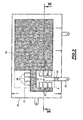
- the figure 2 represents a switching cell, designated by the general reference 20, corresponding to the electrical diagram of the figure 1 .
- This cell is formed of a substrate 22 of substantially parallelepipedal dielectric material inside which are incorporated transistors 4 to 6 and diodes 10 to 12 of the figure 1 .
- the substrate 22 is formed by a stack of 4 horizontal blades 24 to 27 of dielectric and thermally conductive material such as alumina, aluminum nitride or diamond. Inside each plate 25 to 27 are incorporated a transistor and its anti-parallel diode. More precisely, the blades 25, 26 and 27 respectively incorporate the transistor 6 and its diode 12, the transistor 5 and its diode 11, and the transistor 4 and its diode 10.
- Each blade 24 to 27 has the shape of a rectangular parallelepiped on the upper face of which are engraved electric tracks which will be described in more detail with regard to the figure 3 .
- a group, respectively 30 to 33, of channels for circulating a cooling fluid On the lower face of each of these blades 24 to 27 is formed a group, respectively 30 to 33, of channels for circulating a cooling fluid. These channels pass right through the substrate 22 from the front face to the rear face of the parallelepiped and extend parallel to the side faces of the substrate 22.
- each group has eight channels spaced apart from each other. other than 2 mm and 0.5 mm deep.
- connection tongues 36 to 38 respectively connected to the gates of transistors 4 to 6 protrude horizontally outwardly from the front face of substrate 22.
- the cell 20 also comprises power connection tongues 42 and 44 respectively connected to the collector of the transistor 6 and to the emitter of the transistor 4. These tongues 42 and 44 protrude outwards from opposite faces of the substrate 22, that is to say here the vertical face of the left side and the vertical face of the right side of the substrate 22.
- the tabs 36 to 38 are intended to be connected to a control unit for switching the transistors 4 to 6.
- the tabs 42 and 44 they are respectively intended to be connected to the potentials Vs and Ve.
- the substrate 22 comprises connecting layers for rigidly securing the blades to each other, which will be described in more detail with respect to the figure 4 .
- the figure 3 represents a view from above of the upper face of the blade 25.
- the two dashed squares respectively represent the location where are incorporated in this plate 25 the transistor 6 and the anti-parallel diode 12.
- the track 50 extends from a point 54 of connection to the gate of the transistor 6 to a point of connection with the tongue 36.
- the track 52 is intended to connect the emitter of the transistor 6 and the anode of the diode 12 to the collector of the transistor 5 and to the cathode of the diode 11 to form the intermediate connection 8.
- the track 52 is extends from points 56 of connection to the emitter of the transistor 6 and points 58 of connection to the anode of the diode 12.
- the track 52 has, moreover, a sufficiently large area for the collector of the transistor 5 can be welded on it as well as the cathode of the diode 11.
- the surface of the track 52 is chosen as large as possible to diffuse and dissipate the heat of the transistor 5.
- the figure 4 represents a vertical section along the line IV-IV of the substrate 22.
- each transistor 4, 5, 6 is incorporated in a blade of dielectric material, for example by implementing the method described in the article of the previously referenced CPES.
- the power components incorporated in these blades each have an upper face and a lower face equipped with respective connection terminals.
- the upper face comprises a terminal 60 for connection to the gate of the transistor and six terminals 62 for connection to the emitter of the transistor. In this sectional view, only two terminals 62 are visible for each transistor.
- each transistor comprises a transistor transistor connection terminal 64 extending substantially over the entire lower surface of the transistor.
- diodes 10 to 12 are in the form of a component having an upper face carrying three connection terminals of the anode and a lower face carrying a connection terminal of the cathode (not shown). Only the connection of the transistors to each other is shown in detail on the figure 4 . The connection of the diodes in series is similar to that of the transistors and is deduced from the explanations given below.
- a transistor and its diode connected in anti-parallel position incorporated in the same blade form a group of components. These groups are arranged alternately to the right and left of a median vertical plane 72 so that it is possible to have a group of channels for circulating a cooling fluid below each successive group in the chain. 2.
- the plane 72 is perpendicular to the plane of the figure 4 .
- the transistors 4 and 6 are arranged on the left of this plane while the transistor 5 is arranged on the right.
- the collector 64 of the transistor 5 and the cathode of the diode 11 are brazed on the track 52 of the blade 25 to the right of the plane 72.
- the collector 64 of the transistor 4 and the cathode of the diode 10 are brazed on a track 70 etched on the upper face of the blade 26.
- the upper face of the blade 26 is symmetrical with the upper face of the blade 25 relative to the plane 72 so that the track 70 forms the intermediate connection 7.
- the upper face of the blade 27 located at the upper end of the stack is identical to that of the blade 26 except that the track connected to the emitter of the transistor 4 is also connected to the tongue 44 and that no transistor or diode is brazed on this face.
- Each group of channels 30 to 33 is here dug in the corresponding blade from the underside thereof located just below where the transistor and the diode are welded on its upper face.
- the blades 24 to 27 are all of constant thickness equal to 1 millimeter or more and the transistors 4 to 6 are all identical and have a thickness of about 500 microns.
- the thickness of the tracks 52, 68 and 70 is here 100 micrometers.
- Each transistor and diode are housed in respective holes 73 through the blade in which they are incorporated. Inside their respective holes, the transistor and the diode are arranged so that the terminal 64, respectively the cathode, is flush with the lower face of this blade. On the contrary, the terminals 60 and 62 of the transistor, respectively the anode of the diode, are located in a plane parallel to the upper face but situated below the level of the upper face so that the terminals 60 and 62 as well that the anode are fully incorporated inside the blade. The transistors and the diodes are fixed in this position by means of an insulating resin 74 disposed between the outer surface of the transistor and the diode and the inner surface of the holes 73 in which they are housed.
- This insulating resin 74 is also spread between two successive blades of the stack so as to electrically isolate the tracks 52, 68 and 70 and the connection points 54, 56 of the external environment.
- this insulating resin deposit provides electrical insulation between the connection points 54 and 56 and the groups of cooling fluid circulation channels.
- connection points 54, 56 and 58 are formed by a deposition of conductive material between on the one hand the connection terminals on the upper face of the transistor or the diode and on the other the corresponding tracks engraved on the upper face of this blade.
- connection point comprises a vertical rectilinear portion corresponding to a well filled with conductive material.
- a well 82 is formed between the upper face of the blade in which a transistor is incorporated and the connection terminals 62 of this transistor.
- a well 80 is formed between the upper face of each blade incorporating a transistor and the connection terminal 60 of the gate of this transistor.
- a method of manufacturing the switching cell 20 will now be described with regard to the method of the figure 5 and Figures 6A to 6F in the particular case of a switching cell comprising three transistors connected in series.
- the process takes place in two main phases. First, a phase 100 for manufacturing standard elementary blocks followed by a phase 102 for assembling these elementary blocks to form the cell 20.
- phase 100 of the base blocks corresponding to the blade 24 associated with the transistor 6 and the diode 12 are manufactured during a step 104.
- a conventional support of electrical components is cut, in an operation 105, to a standard format.
- Such a conventional support is in the form of a layer of dielectric material having a coppered upper face to be etched.
- the group 30 of channels is dug, during an operation 106, on the underside of the support.
- the coppered surface of the plate is etched, during an operation 108, to form the track 68 and the transistor 6 and the diode 12 are brazed during an operation 110 on the track 68.
- the tongue 42 is also welded with track 68.
- step 116 of making intermediate bricks is performed.
- This step 116 comprises the same operations as step 104 as well as an additional operation 114 of cutting in the support the two holes 73 each intended to receive a transistor or a diode. These holes pass right through the thickness of the support and are formed on the side opposite to that where the transistor and the diode are soldered.
- no tab 42 is welded.
- step 116 an intermediate brick represented on the Figure 6B corresponding for example to the blade 25 associated with the transistor 5 of the figure 4 .
- a step 118 of making end bricks to be placed at the upper end of the stack of blades is performed.
- This step 118 is identical to step 104 except that step 110 is replaced by step 114 and an operation 119 for connecting the connection tab 44 is performed.
- an end brick similar to the blade 27 associated with the tongue 44 is obtained.
- a layer of the insulating resin 74 is deposited, during a step 120, on the upper face of the base brick so as to electrically isolate the track 68 from the external environment.
- this layer is intended to electrically isolate the track 68 from the group of channels 31.
- glue (not shown) is distributed during a step 121, on the upper face of the basic brick. This glue is arranged to ensure the attachment on this upper face of an intermediate brick.
- an intermediate brick is stacked, in a step 122, on the base brick so that the soldered transistor on the base brick is housed inside the hole 73 formed in the intermediate brick.
- step 122 the assembly of the Figure 6C is obtained, this assembly corresponding for example to the stack of the blade 25 on the blade 24.
- the resin 74 of insulating dielectric material such as an epoxy resin, is deposited, during a step 124, inside the hole 73 in which the transistor 6 is housed to electrically isolate the latter from its environment and, when in a step 126, the wells 80 and 82 are hollowed out in the insulating resin.
- This step 126 is for example carried out by a screen printing process or a process known as "dispensing".
- the assembly obtained at the end of this step 126 is that of the Figure 6D .
- Copper is then deposited, during a step 128, in the wells 80 and 82 as well as on the upper face of the blade 25 so as to form the connection points 54, 56 and 58 with the corresponding tracks engraved on the face
- FIG. figure 6E The result obtained at the end of this step is shown in FIG. figure 6E .
- a new layer of the resin 74 is spread on the upper face of the blade 25 so as to isolate the tracks and electrical connection points and ensure the flatness of the upper face of the stack intended to receive the next brick.
- steps 121 to 130 are repeated in the particular case of stacking a new intermediate brick on those already stacked. Steps 121 to 130 are thus repeated as many times as there are components in the chain 2, that is to say here three times in all. It will be noted, however, that during the last iteration of steps 121 to 130, it is not an intermediate brick which is stacked in a manner similar to that described with respect to steps 121 to 130 but an end brick.
- a switching cell manufactured for example according to the method of figure 5 also has the advantage of having groups of circulation of cooling fluid arranged above and below each power component so that these power components are cooled both by their lower face and their upper face. As a result, the cooling of the power components is more efficient and the electrical performance of the cell is improved.
- the cell 20 has been described here in the particular case where the intermediate connections 7 and 8 are not accessible from the outside of the substrate 22.
- a tab projecting from the rear face of the substrate 22 is connected to this intermediate connection.
- Such a variant is particularly advantageous when the cell has an even number of transistors in series and when this additional tab is connected to the intermediate connection located in the middle of the chain so as to form a midpoint.
- Such a switching cell then alone forms an arm of an inverter.
- the cell 20 has been described here in the particular case where the power components are formed of diodes and transistors. However, alternatively, these components may be replaced by other components suitable for switching currents or voltages such as for example thyristors.
Landscapes
- Inverter Devices (AREA)
- Rectifiers (AREA)
- Junction Field-Effect Transistors (AREA)
- Electrical Discharge Machining, Electrochemical Machining, And Combined Machining (AREA)
- General Induction Heating (AREA)
Claims (16)
- Leistungsschaltungszelle, die aufweist: mindestens zwei Leistungskomponenten (4 bis 6), die in einem dielektrischen Substrat (22) aufgenommen sind und jeweils aufweisen: eine erste Fläche, die mit mindestens einer elektrischen Anschlussklemme (64) versehen ist, und eine zweite entgegengesetzte Fläche, die mit mindestens einer anderen elektrischen Anschlussklemme (60, 62) versehen ist, wobei die Komponenten (4 bis 6) eine Kette (2) von Komponenten bilden, die mittels mindestens einer Zwischenschaltung (7, 8), die vollständig im Inneren des Substrates (22) aufgenommen ist, elektrisch in Reihe geschaltet sind, wobei jede Zwischenschaltung die zweite Fläche der vorangehenden Komponente elektrisch an die erste Fläche der in der Kette (2) folgenden Komponente anschließt, wobei die nicht an eine Zwischenschaltung (7, 8) angeschlossenen Flächen der an den äußeren Enden der Kette positionierten Komponenten derart angeordnet sind, dass sie mittels des dielektrischen Materials, welches das Substrat (22) bildet, voneinander getrennt sind, dadurch gekennzeichnet, dass das Substrat (22) aus einem Stapel von parallelen Blättern (24 bis 27) aus einem dielektrischen Material gebildet ist, und dass jede der Komponenten (4 bis 6), die in der Kette (2) aufeinander folgen, in der Dicke eines anderen Blatts aufgenommen ist.
- Zelle gemäß Anspruch 1, dadurch gekennzeichnet, dass die nicht an eine Zwischenschaltung (7, 8) angeschlossenen Flächen der an den äußeren Enden der Kette (2) positionierten Komponenten in unterschiedliche Richtungen ausgerichtet sind, so dass der kürzeste Weg zwischen den beiden Flächen das dielektrische Material durchquert, welches das Substrat (22) bildet, in dem sie aufgenommen sind.
- Zelle gemäß Anspruch 1, dadurch gekennzeichnet, dass die erste und die zweite Fläche jeder Komponente (4 bis 6) parallel zu den Flächen des Blattes sind, in das die Komponente aufgenommen ist.
- Zelle gemäß Anspruch 3, dadurch gekennzeichnet, dass mindestens eine der ersten und der zweiten Fläche jeder Komponente (4 bis 6) auf einer Seite des Blattes, in das die Komponente aufgenommen ist, bündig eingelassen ist.
- Zelle gemäß einem der Ansprüche 1 bis 4, dadurch gekennzeichnet, dass die Zwischenschaltung (7, 8) zwischen zwei Komponenten durch eine elektrische Bahn (52, 70) gebildet ist, die in mindestens eine der Flächen des Blattes, in das die eine der beiden Komponenten aufgenommen ist, eingeätzt ist.
- Zelle gemäß Anspruch 5, dadurch gekennzeichnet, dass mindestens eine der beiden Komponenten (4, 5) der Kette an die eingeätzte elektrische Bahn (52, 70) angeschweißt ist.
- Zelle gemäß einem der vorhergehenden Ansprüche, dadurch gekennzeichnet, dass sie mindestens einen Kanal (30 bis 33) für die Zirkulation einer Kühlflüssigkeit aufweist, der im Inneren des Substrates vorgesehen ist, zum Kühlen von mindestens einer der in dem Substrat aufgenommenen Komponenten.
- Zelle gemäß Anspruch 7, dadurch gekennzeichnet, dass sie mehrere Kanäle für das Zirkulieren einer Kühlflüssigkeit aufweist, und dass jede Leistungskomponente zwischen mindestens zwei der Kanäle angeordnet ist, so dass ihre erste und ihre zweite Fläche durch die Kanäle gekühlt werden.
- Zelle gemäß den Ansprüchen 1 und 8 in Kombination, dadurch gekennzeichnet, dass sie mindestens einen Kanal (30 bis 33) für das Zirkulieren einer Kühlflüssigkeit aufweist, der in jedem Blatt (24 bis 27) ausgebildet ist, welches das Substrat bildet.
- Zelle gemäß den Ansprüchen 6 und 9 in Kombination, dadurch gekennzeichnet, dass der mindestens eine Kanal (30 bis 33), der in jedem Blatt ausgebildet ist, unterhalb der oder jeder auf die Fläche des Blattes geschweißten Komponente positioniert ist.
- Zelle gemäß einem der vorhergehenden Ansprüche, dadurch gekennzeichnet, dass:- das Substrat (22) mindestens eine erste und eine zweite entgegengesetzte Fläche aufweist,- die Zelle aufweist: eine elektrische Anschlusslasche (42), die an die erste Fläche der ersten Komponente (6) der Kette (2) angeschlossen ist, und eine zweite elektrische Anschlusslasche (44), die an die zweite Fläche der letzten Komponente (4) der Kette (2) angeschlossen ist, und- dass die erste und die zweite Lasche (42, 44) jeweils von der ersten und der zweiten entgegengesetzten Fläche hervorstehen.
- Zelle gemäß Anspruch 11, dadurch gekennzeichnet, dass:- das Substrat (22) eine dritte Fläche aufweist, die sich von der ersten und der zweiten Fläche unterscheidet,- die Zelle mindestens eine dritte elektrische Anschlusslasche aufweist, die an eine Zwischenschaltung (7, 8) angeschlossen ist, und- dass die dritte Lasche von der dritten Fläche hervorsteht.
- Zelle gemäß einem der vorhergehenden Ansprüche, dadurch gekennzeichnet, dass die Komponenten Leistungstransistoren sind.
- Zelle gemäß einem der vorhergehenden Ansprüche, dadurch gekennzeichnet, dass das Substrat parallelepipedförmig ist.
- Zelle gemäß einem der vorhergehenden Ansprüche, dadurch gekennzeichnet, dass die Blätter (24 bis 27), die die Komponenten aufnehmen, alle eine identische Größe aufweisen.
- Verfahren zur Herstellung einer Schaltungszelle gemäß einem der vorhergehenden Ansprüche, dadurch gekennzeichnet, dass es aufweist:- eine Phase (100) der Herstellung von elementaren Blöcken, wobei jeder elementare Block aus einem Blatt (25 bis 26) des Substrats gebildet wird, auf welches eine der Leistungskomponenten (4 bis 7) geschweißt wird, und in welchem ein Durchgangsloch (73) vorgesehen wird, das zum Aufnehmen der Leistungskomponente eines anderen identischen elementaren Blocks bestimmt ist, und- eine Montage-Phase (102), während der die elementaren Blöcke zum Ausbilden der Schaltungszelle aufeinander gestapelt werden.
Applications Claiming Priority (2)
| Application Number | Priority Date | Filing Date | Title |
|---|---|---|---|
| FR0306748 | 2003-06-04 | ||
| FR0306748A FR2855912B1 (fr) | 2003-06-04 | 2003-06-04 | Cellule de commutation de puissance, et procede de fabrication de la cellule |
Publications (2)
| Publication Number | Publication Date |
|---|---|
| EP1484797A1 EP1484797A1 (de) | 2004-12-08 |
| EP1484797B1 true EP1484797B1 (de) | 2009-04-15 |
Family
ID=33155654
Family Applications (1)
| Application Number | Title | Priority Date | Filing Date |
|---|---|---|---|
| EP04300311A Expired - Lifetime EP1484797B1 (de) | 2003-06-04 | 2004-06-02 | Leistungswechselrichter und dessen Herstellung |
Country Status (6)
| Country | Link |
|---|---|
| US (1) | US6995409B2 (de) |
| EP (1) | EP1484797B1 (de) |
| AT (1) | ATE429034T1 (de) |
| DE (1) | DE602004020541D1 (de) |
| ES (1) | ES2325921T3 (de) |
| FR (1) | FR2855912B1 (de) |
Families Citing this family (7)
| Publication number | Priority date | Publication date | Assignee | Title |
|---|---|---|---|---|
| US7298034B2 (en) * | 2004-06-28 | 2007-11-20 | Semiconductor Components Industries, L.L.C. | Multi-chip semiconductor connector assemblies |
| US7202106B2 (en) | 2004-06-28 | 2007-04-10 | Semiconductor Components Industries, L.L.C. | Multi-chip semiconductor connector and method |
| ATE393475T1 (de) * | 2004-11-24 | 2008-05-15 | Danfoss Silicon Power Gmbh | Strömungsverteilungsmodul und stapel von strömungsverteilungsmodulen |
| GB2442622B (en) * | 2006-08-04 | 2009-06-24 | Clean Current Power Systems Inc | Rotor and stator segments for generator and motor |
| KR100807980B1 (ko) | 2006-11-27 | 2008-02-28 | 동부일렉트로닉스 주식회사 | 반도체 소자 및 그 제조 방법 |
| US7773381B2 (en) * | 2007-09-26 | 2010-08-10 | Rohm Co., Ltd. | Semiconductor device |
| CN112908943A (zh) * | 2021-01-12 | 2021-06-04 | 华为技术有限公司 | 一种埋入式封装结构及其制备方法、终端设备 |
Family Cites Families (6)
| Publication number | Priority date | Publication date | Assignee | Title |
|---|---|---|---|---|
| DE4421319A1 (de) * | 1994-06-17 | 1995-12-21 | Abb Management Ag | Niederinduktives Leistungshalbleitermodul |
| US6060795A (en) * | 1998-03-18 | 2000-05-09 | Intersil Corporation | Semiconductor power pack |
| EP2244289B1 (de) * | 2000-04-19 | 2014-03-26 | Denso Corporation | Kühlmittelgekühltes Halbleiterbauelement |
| JP3894413B2 (ja) * | 2000-06-08 | 2007-03-22 | 三菱電機株式会社 | 車両用交流発電機 |
| JP2002026251A (ja) * | 2000-07-11 | 2002-01-25 | Toshiba Corp | 半導体装置 |
| EP1318547B1 (de) * | 2001-12-06 | 2013-04-17 | ABB Research Ltd. | Leistungshalbleiter-Modul |
-
2003
- 2003-06-04 FR FR0306748A patent/FR2855912B1/fr not_active Expired - Fee Related
-
2004
- 2004-06-01 US US10/858,293 patent/US6995409B2/en not_active Expired - Lifetime
- 2004-06-02 EP EP04300311A patent/EP1484797B1/de not_active Expired - Lifetime
- 2004-06-02 ES ES04300311T patent/ES2325921T3/es not_active Expired - Lifetime
- 2004-06-02 DE DE602004020541T patent/DE602004020541D1/de not_active Expired - Lifetime
- 2004-06-02 AT AT04300311T patent/ATE429034T1/de active
Also Published As
| Publication number | Publication date |
|---|---|
| FR2855912A1 (fr) | 2004-12-10 |
| EP1484797A1 (de) | 2004-12-08 |
| US6995409B2 (en) | 2006-02-07 |
| ES2325921T3 (es) | 2009-09-24 |
| US20050017264A1 (en) | 2005-01-27 |
| FR2855912B1 (fr) | 2006-04-14 |
| ATE429034T1 (de) | 2009-05-15 |
| DE602004020541D1 (de) | 2009-05-28 |
Similar Documents
| Publication | Publication Date | Title |
|---|---|---|
| EP1025584B1 (de) | Elektronische integrierte schaltung mit mindestens einem elektronischen bauelement | |
| EP1158656B1 (de) | Elektronische Leistungsvorrichtung | |
| WO2011004081A1 (fr) | Module electronique de puissance | |
| EP3216056B1 (de) | Elektronische leistungsvorrichtung mit vertikaler 3d-schaltzelle | |
| EP1484797B1 (de) | Leistungswechselrichter und dessen Herstellung | |
| FR3065319A1 (fr) | Module electronique de puissance et convertisseur electrique de puissance l’incorporant | |
| EP2288001A1 (de) | Wechselstromgenerator mit synchroner Gleichrichtung, der mit einem perfektionierten elektronischen Leistungsmodul ausgestattet ist | |
| FR2816462A1 (fr) | Module convertisseur de puissance et dispositif convertisseur de puissance pour moteur a phases multiples avec pour chaque phase un tel module convertisseur de puissance | |
| EP3242322B1 (de) | Elektronische leistungsvorrichtung mit flacher elektrischer verbindungsstruktur | |
| EP1114456A1 (de) | Gemeinsames verfahren zum herstellen einer mehrzahl von bauelementen welche ursprünglich in dasselbe substrat geformt sind | |
| EP2288002A1 (de) | Wechselstromgenerator mit synchroner Gleichrichtung, der mit einem perfektionierten elektronischen Leistungsmodul ausgestattet ist | |
| EP1032114B1 (de) | Elektrisches Modul für Fahrzeug-, insbesondere Autolichtmaschine, und ein solches Modul und eine solche Lichtmaschine beinhaltende Anordnung | |
| FR3105651A1 (fr) | Distributeur électrique | |
| EP2660978A1 (de) | Vorrichtung, die eine elektronische Komponente mit hoher Schaltgeschwindigkeit umfasst | |
| EP1329954A1 (de) | Matrixumrichter zur Umwandlung elektrischer Energie | |
| EP2319080A1 (de) | Dreidimensionale cmos-schaltung auf zwei versetzten substraten sowie verfahren zu ihrer herstellung | |
| EP3288185B1 (de) | Elektrisches schaltgerät, das mit einer verbesserten elektrischen verbindungsvorrichtung ausgestattet ist | |
| EP4572112A1 (de) | Leistungsmodul und statischer stromwandler | |
| FR3119930A1 (fr) | Module électronique de puissance | |
| EP4690304A1 (de) | Leistungsmodul | |
| EP3360160A1 (de) | Elektronisches strommodul | |
| FR2827424A1 (fr) | Composant electronique encapsule comportant un dispositif electronique de puissance et procede de fabrication | |
| EP2500937B1 (de) | Elektronischer Schaltkreis mit Doppelisolierschicht, und sein Herstellungsverfahren | |
| FR3103316A1 (fr) | Cadre métallique conducteur pour module électronique de puissance et procédé de fabrication associé | |
| WO2023110966A1 (fr) | Bras de commutation utilisant une carte de circuit imprimé |
Legal Events
| Date | Code | Title | Description |
|---|---|---|---|
| PUAI | Public reference made under article 153(3) epc to a published international application that has entered the european phase |
Free format text: ORIGINAL CODE: 0009012 |
|
| AK | Designated contracting states |
Kind code of ref document: A1 Designated state(s): AT BE BG CH CY CZ DE DK EE ES FI FR GB GR HU IE IT LI LU MC NL PL PT RO SE SI SK TR |
|
| AX | Request for extension of the european patent |
Extension state: AL HR LT LV MK |
|
| 17P | Request for examination filed |
Effective date: 20050608 |
|
| AKX | Designation fees paid |
Designated state(s): AT BE BG CH CY CZ DE DK EE ES FI FR GB GR HU IE IT LI LU MC NL PL PT RO SE SI SK TR |
|
| RAP1 | Party data changed (applicant data changed or rights of an application transferred) |
Owner name: ALSTOM TRANSPORT SA |
|
| GRAP | Despatch of communication of intention to grant a patent |
Free format text: ORIGINAL CODE: EPIDOSNIGR1 |
|
| GRAS | Grant fee paid |
Free format text: ORIGINAL CODE: EPIDOSNIGR3 |
|
| GRAA | (expected) grant |
Free format text: ORIGINAL CODE: 0009210 |
|
| AK | Designated contracting states |
Kind code of ref document: B1 Designated state(s): AT BE BG CH CY CZ DE DK EE ES FI FR GB GR HU IE IT LI LU MC NL PL PT RO SE SI SK TR |
|
| REG | Reference to a national code |
Ref country code: CH Ref legal event code: EP Ref country code: GB Ref legal event code: FG4D Free format text: NOT ENGLISH |
|
| REG | Reference to a national code |
Ref country code: IE Ref legal event code: FG4D |
|
| REF | Corresponds to: |
Ref document number: 602004020541 Country of ref document: DE Date of ref document: 20090528 Kind code of ref document: P |
|
| REG | Reference to a national code |
Ref country code: SE Ref legal event code: TRGR |
|
| REG | Reference to a national code |
Ref country code: ES Ref legal event code: FG2A Ref document number: 2325921 Country of ref document: ES Kind code of ref document: T3 |
|
| NLV1 | Nl: lapsed or annulled due to failure to fulfill the requirements of art. 29p and 29m of the patents act | ||
| PG25 | Lapsed in a contracting state [announced via postgrant information from national office to epo] |
Ref country code: PT Free format text: LAPSE BECAUSE OF FAILURE TO SUBMIT A TRANSLATION OF THE DESCRIPTION OR TO PAY THE FEE WITHIN THE PRESCRIBED TIME-LIMIT Effective date: 20090915 Ref country code: FI Free format text: LAPSE BECAUSE OF FAILURE TO SUBMIT A TRANSLATION OF THE DESCRIPTION OR TO PAY THE FEE WITHIN THE PRESCRIBED TIME-LIMIT Effective date: 20090415 |
|
| PG25 | Lapsed in a contracting state [announced via postgrant information from national office to epo] |
Ref country code: SI Free format text: LAPSE BECAUSE OF FAILURE TO SUBMIT A TRANSLATION OF THE DESCRIPTION OR TO PAY THE FEE WITHIN THE PRESCRIBED TIME-LIMIT Effective date: 20090415 Ref country code: PL Free format text: LAPSE BECAUSE OF FAILURE TO SUBMIT A TRANSLATION OF THE DESCRIPTION OR TO PAY THE FEE WITHIN THE PRESCRIBED TIME-LIMIT Effective date: 20090415 Ref country code: NL Free format text: LAPSE BECAUSE OF FAILURE TO SUBMIT A TRANSLATION OF THE DESCRIPTION OR TO PAY THE FEE WITHIN THE PRESCRIBED TIME-LIMIT Effective date: 20090415 |
|
| REG | Reference to a national code |
Ref country code: HU Ref legal event code: AG4A Ref document number: E005992 Country of ref document: HU |
|
| REG | Reference to a national code |
Ref country code: IE Ref legal event code: FD4D |
|
| BERE | Be: lapsed |
Owner name: ALSTOM TRANSPORT SA Effective date: 20090630 |
|
| PG25 | Lapsed in a contracting state [announced via postgrant information from national office to epo] |
Ref country code: EE Free format text: LAPSE BECAUSE OF FAILURE TO SUBMIT A TRANSLATION OF THE DESCRIPTION OR TO PAY THE FEE WITHIN THE PRESCRIBED TIME-LIMIT Effective date: 20090415 Ref country code: MC Free format text: LAPSE BECAUSE OF NON-PAYMENT OF DUE FEES Effective date: 20090630 Ref country code: IE Free format text: LAPSE BECAUSE OF FAILURE TO SUBMIT A TRANSLATION OF THE DESCRIPTION OR TO PAY THE FEE WITHIN THE PRESCRIBED TIME-LIMIT Effective date: 20090415 Ref country code: CZ Free format text: LAPSE BECAUSE OF FAILURE TO SUBMIT A TRANSLATION OF THE DESCRIPTION OR TO PAY THE FEE WITHIN THE PRESCRIBED TIME-LIMIT Effective date: 20090415 Ref country code: DK Free format text: LAPSE BECAUSE OF FAILURE TO SUBMIT A TRANSLATION OF THE DESCRIPTION OR TO PAY THE FEE WITHIN THE PRESCRIBED TIME-LIMIT Effective date: 20090415 Ref country code: RO Free format text: LAPSE BECAUSE OF FAILURE TO SUBMIT A TRANSLATION OF THE DESCRIPTION OR TO PAY THE FEE WITHIN THE PRESCRIBED TIME-LIMIT Effective date: 20090415 |
|
| REG | Reference to a national code |
Ref country code: CH Ref legal event code: PL |
|
| PLBE | No opposition filed within time limit |
Free format text: ORIGINAL CODE: 0009261 |
|
| STAA | Information on the status of an ep patent application or granted ep patent |
Free format text: STATUS: NO OPPOSITION FILED WITHIN TIME LIMIT |
|
| PG25 | Lapsed in a contracting state [announced via postgrant information from national office to epo] |
Ref country code: SK Free format text: LAPSE BECAUSE OF FAILURE TO SUBMIT A TRANSLATION OF THE DESCRIPTION OR TO PAY THE FEE WITHIN THE PRESCRIBED TIME-LIMIT Effective date: 20090415 |
|
| 26N | No opposition filed |
Effective date: 20100118 |
|
| GBPC | Gb: european patent ceased through non-payment of renewal fee |
Effective date: 20090715 |
|
| REG | Reference to a national code |
Ref country code: FR Ref legal event code: ST Effective date: 20100226 |
|
| PG25 | Lapsed in a contracting state [announced via postgrant information from national office to epo] |
Ref country code: BG Free format text: LAPSE BECAUSE OF FAILURE TO SUBMIT A TRANSLATION OF THE DESCRIPTION OR TO PAY THE FEE WITHIN THE PRESCRIBED TIME-LIMIT Effective date: 20090715 |
|
| PG25 | Lapsed in a contracting state [announced via postgrant information from national office to epo] |
Ref country code: CH Free format text: LAPSE BECAUSE OF NON-PAYMENT OF DUE FEES Effective date: 20090630 Ref country code: LI Free format text: LAPSE BECAUSE OF NON-PAYMENT OF DUE FEES Effective date: 20090630 Ref country code: FR Free format text: LAPSE BECAUSE OF NON-PAYMENT OF DUE FEES Effective date: 20090630 |
|
| PG25 | Lapsed in a contracting state [announced via postgrant information from national office to epo] |
Ref country code: GB Free format text: LAPSE BECAUSE OF NON-PAYMENT OF DUE FEES Effective date: 20090715 |
|
| PG25 | Lapsed in a contracting state [announced via postgrant information from national office to epo] |
Ref country code: BE Free format text: LAPSE BECAUSE OF NON-PAYMENT OF DUE FEES Effective date: 20090630 |
|
| PG25 | Lapsed in a contracting state [announced via postgrant information from national office to epo] |
Ref country code: GR Free format text: LAPSE BECAUSE OF FAILURE TO SUBMIT A TRANSLATION OF THE DESCRIPTION OR TO PAY THE FEE WITHIN THE PRESCRIBED TIME-LIMIT Effective date: 20090716 |
|
| PG25 | Lapsed in a contracting state [announced via postgrant information from national office to epo] |
Ref country code: LU Free format text: LAPSE BECAUSE OF NON-PAYMENT OF DUE FEES Effective date: 20090602 |
|
| PG25 | Lapsed in a contracting state [announced via postgrant information from national office to epo] |
Ref country code: TR Free format text: LAPSE BECAUSE OF FAILURE TO SUBMIT A TRANSLATION OF THE DESCRIPTION OR TO PAY THE FEE WITHIN THE PRESCRIBED TIME-LIMIT Effective date: 20090415 |
|
| PG25 | Lapsed in a contracting state [announced via postgrant information from national office to epo] |
Ref country code: CY Free format text: LAPSE BECAUSE OF FAILURE TO SUBMIT A TRANSLATION OF THE DESCRIPTION OR TO PAY THE FEE WITHIN THE PRESCRIBED TIME-LIMIT Effective date: 20090415 |
|
| REG | Reference to a national code |
Ref country code: HU Ref legal event code: FH1C Free format text: FORMER REPRESENTATIVE(S): DR. HARANGOZO GABOR, DANUBIA SZABADALMI ES JOGI IRODA KFT., HU Representative=s name: DANUBIA SZABADALMI ES JOGI IRODA KFT., HU Ref country code: HU Ref legal event code: GB9C Owner name: ALSTOM TRANSPORT TECHNOLOGIES, FR Free format text: FORMER OWNER(S): ALSTOM TRANSPORT S.A., FR Ref country code: DE Ref legal event code: R081 Ref document number: 602004020541 Country of ref document: DE Owner name: ALSTOM TRANSPORT TECHNOLOGIES, FR Free format text: FORMER OWNER: ALSTOM TRANSPORT S.A., LEVALLOIS-PERRET, FR |
|
| REG | Reference to a national code |
Ref country code: HU Ref legal event code: HC9C Owner name: ALSTOM TRANSPORT TECHNOLOGIES, FR Free format text: FORMER OWNER(S): ALSTOM TRANSPORT S.A., FR; ALSTOM TRANSPORT TECHNOLOGIES, FR |
|
| REG | Reference to a national code |
Ref country code: DE Ref legal event code: R081 Ref document number: 602004020541 Country of ref document: DE Owner name: ALSTOM TRANSPORT TECHNOLOGIES, FR Free format text: FORMER OWNER: ALSTOM TRANSPORT TECHNOLOGIES, LEVALLOIS-PERRET, FR |
|
| REG | Reference to a national code |
Ref country code: AT Ref legal event code: PC Ref document number: 429034 Country of ref document: AT Kind code of ref document: T Owner name: ALSTOM TRANSPORT TECHNOLOGIES, FR Effective date: 20180220 |
|
| PGFP | Annual fee paid to national office [announced via postgrant information from national office to epo] |
Ref country code: DE Payment date: 20200618 Year of fee payment: 17 |
|
| PGFP | Annual fee paid to national office [announced via postgrant information from national office to epo] |
Ref country code: SE Payment date: 20200625 Year of fee payment: 17 |
|
| PGFP | Annual fee paid to national office [announced via postgrant information from national office to epo] |
Ref country code: AT Payment date: 20200619 Year of fee payment: 17 |
|
| PGFP | Annual fee paid to national office [announced via postgrant information from national office to epo] |
Ref country code: ES Payment date: 20200824 Year of fee payment: 17 |
|
| PGFP | Annual fee paid to national office [announced via postgrant information from national office to epo] |
Ref country code: IT Payment date: 20200625 Year of fee payment: 17 Ref country code: HU Payment date: 20200718 Year of fee payment: 17 |
|
| REG | Reference to a national code |
Ref country code: DE Ref legal event code: R119 Ref document number: 602004020541 Country of ref document: DE |
|
| REG | Reference to a national code |
Ref country code: SE Ref legal event code: EUG |
|
| REG | Reference to a national code |
Ref country code: AT Ref legal event code: MM01 Ref document number: 429034 Country of ref document: AT Kind code of ref document: T Effective date: 20210602 |
|
| PG25 | Lapsed in a contracting state [announced via postgrant information from national office to epo] |
Ref country code: HU Free format text: LAPSE BECAUSE OF NON-PAYMENT OF DUE FEES Effective date: 20210603 Ref country code: DE Free format text: LAPSE BECAUSE OF NON-PAYMENT OF DUE FEES Effective date: 20220101 Ref country code: AT Free format text: LAPSE BECAUSE OF NON-PAYMENT OF DUE FEES Effective date: 20210602 |
|
| PG25 | Lapsed in a contracting state [announced via postgrant information from national office to epo] |
Ref country code: SE Free format text: LAPSE BECAUSE OF NON-PAYMENT OF DUE FEES Effective date: 20210603 |
|
| PG25 | Lapsed in a contracting state [announced via postgrant information from national office to epo] |
Ref country code: IT Free format text: LAPSE BECAUSE OF NON-PAYMENT OF DUE FEES Effective date: 20210602 |
|
| REG | Reference to a national code |
Ref country code: ES Ref legal event code: FD2A Effective date: 20220801 |
|
| PG25 | Lapsed in a contracting state [announced via postgrant information from national office to epo] |
Ref country code: ES Free format text: LAPSE BECAUSE OF NON-PAYMENT OF DUE FEES Effective date: 20210603 |