EP1484796A2 - Semiconductor device and manufacturing method of the same - Google Patents
Semiconductor device and manufacturing method of the same Download PDFInfo
- Publication number
- EP1484796A2 EP1484796A2 EP04013033A EP04013033A EP1484796A2 EP 1484796 A2 EP1484796 A2 EP 1484796A2 EP 04013033 A EP04013033 A EP 04013033A EP 04013033 A EP04013033 A EP 04013033A EP 1484796 A2 EP1484796 A2 EP 1484796A2
- Authority
- EP
- European Patent Office
- Prior art keywords
- semiconductor
- wafer
- cap
- arrayed
- sealed
- Prior art date
- Legal status (The legal status is an assumption and is not a legal conclusion. Google has not performed a legal analysis and makes no representation as to the accuracy of the status listed.)
- Withdrawn
Links
Images


Classifications
-
- B—PERFORMING OPERATIONS; TRANSPORTING
- B81—MICROSTRUCTURAL TECHNOLOGY
- B81B—MICROSTRUCTURAL DEVICES OR SYSTEMS, e.g. MICROMECHANICAL DEVICES
- B81B7/00—Microstructural systems ; Auxiliary parts of microstructural devices or systems
- B81B7/0032—Packages or encapsulation
- B81B7/007—Interconnections between the MEMS and external electrical signals
-
- H—ELECTRICITY
- H10—SEMICONDUCTOR DEVICES; ELECTRIC SOLID-STATE DEVICES NOT OTHERWISE PROVIDED FOR
- H10F—INORGANIC SEMICONDUCTOR DEVICES SENSITIVE TO INFRARED RADIATION, LIGHT, ELECTROMAGNETIC RADIATION OF SHORTER WAVELENGTH OR CORPUSCULAR RADIATION
- H10F99/00—Subject matter not provided for in other groups of this subclass
-
- H—ELECTRICITY
- H10—SEMICONDUCTOR DEVICES; ELECTRIC SOLID-STATE DEVICES NOT OTHERWISE PROVIDED FOR
- H10F—INORGANIC SEMICONDUCTOR DEVICES SENSITIVE TO INFRARED RADIATION, LIGHT, ELECTROMAGNETIC RADIATION OF SHORTER WAVELENGTH OR CORPUSCULAR RADIATION
- H10F39/00—Integrated devices, or assemblies of multiple devices, comprising at least one element covered by group H10F30/00, e.g. radiation detectors comprising photodiode arrays
- H10F39/80—Constructional details of image sensors
-
- H—ELECTRICITY
- H10—SEMICONDUCTOR DEVICES; ELECTRIC SOLID-STATE DEVICES NOT OTHERWISE PROVIDED FOR
- H10F—INORGANIC SEMICONDUCTOR DEVICES SENSITIVE TO INFRARED RADIATION, LIGHT, ELECTROMAGNETIC RADIATION OF SHORTER WAVELENGTH OR CORPUSCULAR RADIATION
- H10F39/00—Integrated devices, or assemblies of multiple devices, comprising at least one element covered by group H10F30/00, e.g. radiation detectors comprising photodiode arrays
- H10F39/80—Constructional details of image sensors
- H10F39/804—Containers or encapsulations
-
- H—ELECTRICITY
- H10—SEMICONDUCTOR DEVICES; ELECTRIC SOLID-STATE DEVICES NOT OTHERWISE PROVIDED FOR
- H10W—GENERIC PACKAGES, INTERCONNECTIONS, CONNECTORS OR OTHER CONSTRUCTIONAL DETAILS OF DEVICES COVERED BY CLASS H10
- H10W99/00—Subject matter not provided for in other groups of this subclass
-
- B—PERFORMING OPERATIONS; TRANSPORTING
- B81—MICROSTRUCTURAL TECHNOLOGY
- B81C—PROCESSES OR APPARATUS SPECIALLY ADAPTED FOR THE MANUFACTURE OR TREATMENT OF MICROSTRUCTURAL DEVICES OR SYSTEMS
- B81C2203/00—Forming microstructural systems
- B81C2203/01—Packaging MEMS
- B81C2203/0118—Bonding a wafer on the substrate, i.e. where the cap consists of another wafer
-
- H—ELECTRICITY
- H10—SEMICONDUCTOR DEVICES; ELECTRIC SOLID-STATE DEVICES NOT OTHERWISE PROVIDED FOR
- H10F—INORGANIC SEMICONDUCTOR DEVICES SENSITIVE TO INFRARED RADIATION, LIGHT, ELECTROMAGNETIC RADIATION OF SHORTER WAVELENGTH OR CORPUSCULAR RADIATION
- H10F39/00—Integrated devices, or assemblies of multiple devices, comprising at least one element covered by group H10F30/00, e.g. radiation detectors comprising photodiode arrays
- H10F39/80—Constructional details of image sensors
- H10F39/805—Coatings
-
- Y—GENERAL TAGGING OF NEW TECHNOLOGICAL DEVELOPMENTS; GENERAL TAGGING OF CROSS-SECTIONAL TECHNOLOGIES SPANNING OVER SEVERAL SECTIONS OF THE IPC; TECHNICAL SUBJECTS COVERED BY FORMER USPC CROSS-REFERENCE ART COLLECTIONS [XRACs] AND DIGESTS
- Y10—TECHNICAL SUBJECTS COVERED BY FORMER USPC
- Y10S—TECHNICAL SUBJECTS COVERED BY FORMER USPC CROSS-REFERENCE ART COLLECTIONS [XRACs] AND DIGESTS
- Y10S257/00—Active solid-state devices, e.g. transistors, solid-state diodes
- Y10S257/924—Active solid-state devices, e.g. transistors, solid-state diodes with passive device, e.g. capacitor, or battery, as integral part of housing or housing element, e.g. cap
Definitions
- the invention relates to a semiconductor device and a manufacturing method thereof, particularly to a semiconductor device in which devices to be sealed are sealed in a package and a manufacturing method thereof.
- an MEMS device a device using a micro electromechanical system
- a CCD charge coupled device
- an IR sensor a sensor electrically detecting infrared radiation
- Such electronic devices are formed on a semiconductor chip and packaged.
- a package includes a can package in which the electronic devices are sealed with a metal cap and a ceramic package in which the electronic devices are sealed with a ceramic cap.
- a semiconductor chip formed with devices to be sealed such as electronic devices and a cap for sealing the devices to be sealed are independently prepared and then assembled. This makes a mass-manufacturing procedure complex, and accordingly increases a manufacturing cost. Furthermore, a package size becomes large, resulting in an increase in a mounting area of the package on a printed board.
- a semiconductor chip formed with devices to be sealed on its front surface is attached with a sealing cap, the devices to be sealed being sealed in a cavity formed of a space between the semiconductor chip and the sealing cap.
- the device to be sealed is an electronic device such as an MEMS device, an IR sensor, and a CCD, or a micro-sized mechanical device.
- the invention provides a semiconductor device and a manufacturing method thereof which simplifies a manufacturing procedure to reduce a manufacturing cost and reduces a package size when electronic devices are packaged.
- the semiconductor chip is formed with via-holes penetrating therethrough. These via-holes are formed with embedded electrodes.
- the embedded electrodes are connected with the devices to be sealed through wiring.
- the embedded electrodes are connected with electrodes for external connection.
- a plurality of sealing caps and semiconductor chips of the semiconductor device are formed on wafers, attached to each other, and divided into a plurality of packages. This procedure can simplify a mass-manufacturing procedure, and reduce a manufacturing cost of each of the packages.
- via-holes are provided penetrating through the semiconductor chip of each of the packages and embedded electrodes are formed therein, so that bump electrodes can be formed on a bottom of the semiconductor chip. This can miniaturize the package and reduce a mounting area of the package on a printed board.
- a cavity for sealing devices to be sealed is filled with an inert gas or kept vacuum so that life and reliability of the sealed devices can be extended and improved.
- Fig. 1A is a plan view of a semiconductor device of this embodiment.
- Fig. 1B is a cross-sectional view along line X-X of Fig. 1A.
- a plurality of MEMS devices 11A as devices to be sealed (e.g., a relay, a condenser, a coil or a motor) is formed in a region SA (indicated by a dotted line) on a front surface of a semiconductor chip 10A (e.g., silicon chip).
- This region SA includes the MEMS devices 11A that function as a single device. That is, these MEMS devices 11A are electronic and mechanical components of a micro-sized mechanism such as a micro-machine.
- Wiring 12 (e.g. made of Cu, Al, or Al alloy) connected with these MEMS devices 11A is formed extending to a periphery of the region SA.
- the wiring 12 is formed in a procedure of forming the MEMS devices 11A on the semiconductor chip 10A, having a thickness of about 1 ⁇ m.
- a plurality of via-holes 13 is formed right under end portions of the wiring 12 formed extending to the periphery of the region SA, penetrating through the semiconductor chip 10A.
- Each of these via-holes 13 is formed with an embedded electrode 14 (e.g., made of Cu, Al or Al alloy) therein.
- the embedded electrodes 14 are formed by a plating method or a sputtering method, and connected with the wiring 12 of the MEMS devices 11A. Although the embedded electrodes 14 are completely embedded in the via holes 13 in Fig. 1B, the embedded electrodes 14 can be partially embedded therein by adjusting a plating time or a sputtering time.
- the embedded electrodes 14 are formed with bump electrodes 15 (e.g. made of solder) on a back surface of the semiconductor chip 10A. Accordingly, leads of the packaged semiconductor chip 10A are not necessary to be drawn from sides of the semiconductor chip 10A, but can be drawn from the bottom of the semiconductor chip 10A, thereby realizing miniaturization of the package. This can prevent increasing of a mounting area of the package on a printed board.
- bump electrodes 15 e.g. made of solder
- the front surface of the semiconductor chip 10A is attached with a sealing cap 20A made of a glass, a silicon, a ceramic or a resin.
- the semiconductor chip 10A and the sealing cap 20A are attached to each other with an adhesive made of an epoxy resin and the like, with the front surface of the semiconductor chip 10A and a concave portion 21A of the sealing cap 20A (inner surface of the sealing cap 20A) facing each other.
- a cavity CV is formed in a space between the front surface of the semiconductor chip 10A and the concave portion 21A of the sealing cap 20A.
- the MEMS devices 11A are sealed in this cavity CV.
- the thickness d of the sealing cap 20A is approximately several ten to several hundred ⁇ m
- the height h of the cavity CV is approximately several to several ten ⁇ m, although the embodiment is not limited to these values.
- the MEMS devices 11A formed on the front surface of the semiconductor chip 10A are sealed in the cavity CV which is filled with an inert gas (e.g., N 2 ) or kept vacuum.
- an inert gas e.g., N 2
- a surface of the concave portion 21A can be formed with a metal thin film 22A having a filter function of blocking or transmitting light having a predetermined wave length. Handling of such a filter made of a metal thin film, which has been difficult to handle with its low strength, can be facilitated by utilizing the cavity CV for forming such a filter 22A on the surface of the concave portion 21A of the sealing cap 20A.
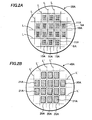
- Fig. 2A is a plan view of a semiconductor wafer 30A formed of the plurality of the semiconductor chips 10A disposed in a matrix.
- the semiconductor wafer 30A is made of a semiconductor material such as silicon.
- the plurality of the semiconductor chips 10A is partitioned with scribe lines L extending in row and column directions.
- the MEMS devices 11A are formed in the region SA, in each of the semiconductor chips 10A.
- the wiring 12 is connected with each of the MEMS devices 11A, extending to the periphery of the region SA.
- Fig. 2B is a plan view of a cap arrayed wafer 40A formed of the above described sealing caps 20A disposed in a matrix.
- the cap arrayed wafer 40A is made of a glass, a silicon, a ceramic or a resin. Each of regions partitioned with scribe lines L' is to face each of the semiconductor chips 10A when attached thereto. These scribe lines L' of the cap arrayed wafer 40A are formed in accordance with the scribe lines L of the semiconductor wafer 30A. The two wafers 30A and 40A are attached so that the scribe lines L' of the cap arrayed wafer 40A are aligned with the scribe lines L of the semiconductor wafer 30A.
- the concave portions 21A are formed on the cap arrayed wafer 40A in the regions corresponding to the regions SA of the semiconductor chips 10A.
- the cap arrayed wafer 40A is made of a glass, a silicon or a ceramic
- the concave portion 21A is formed by etching.
- the cap arrayed wafer 40A is made of a resin
- the cap arrayed wafer 40A is formed by injection molding to have the plurality of the concave portions 21A.
- the embedded electrodes 14 and the bump electrodes 15 serving as electrodes for external connection are connected with the MEMS devices through the wiring 12 in the above described semiconductor chips 10A and the semiconductor wafer 30A, the embedded electrodes 14 and the bump electrodes 15 can be directly connected with the MEMS devices 11A without through the wiring 12. This is applied to a second embodiment described below.
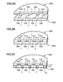
- the semiconductor wafer 30A formed with the MEMS devices and the wiring 12 (not shown) on its front surface is prepared.
- the structure of the semiconductor wafer 30A is the same as the structure shown in Fig. 2A.
- the cap arrayed wafer 40A having the plurality of the concave portion 21A is prepared.
- the structure of the cap arrayed wafer 40A is the same as the structure shown in Fig. 2B.
- the cap arrayed wafer 40A is made of a glass or a silicon, the surface of the concave portion 21A can be formed with the metal thin film 22A having a filter function of blocking or transmitting light having a predetermined wavelength.
- the cap arrayed wafer 40A and the semiconductor wafer 30A are disposed to face the concave portions 21A of the cap arrayed wafer 40A and the front surface of the semiconductor wafer 30A.
- the cap arrayed wafer 40A and the semiconductor wafer 30A are attached with an adhesive made of an epoxy resin or the like. At this time, each of the concave portions 21A of the cap arrayed wafer 40A faces each of the regions SA of the semiconductor wafer 30A.
- the cavity CV is formed in a space between each of the concave portions 21A of the cap arrayed wafer 40A and the front surface of the semiconductor wafer 30A, and the MEMS devices 11A are sealed in this cavity.
- the cap arrayed wafer 40A and the semiconductor wafer 30A are attached in a vacuum atmosphere to maintain the cavity CV in vacuum.
- the cap arrayed wafer 40A and the semiconductor wafer 30A can be attached in an inert gas (e.g., N 2 ) atmosphere to fill the cavity CV with the inert gas.
- the semiconductor wafer 30A is ground on its back surface to make a thickness of the semiconductor wafer 30A several ten to several hundred ⁇ m, for example.
- this back-grinding can be performed to the cap arrayed wafer 40A or both the semiconductor wafer 30A and the cap arrayed wafer 40A.
- the plurality of the via-holes 13 is formed penetrating from the back surface to the front surface of the semiconductor wafer 30A.
- An etching method or a laser beam irradiating method can be used for forming these via-holes 13.
- the embedded electrodes 14 are formed in these via-holes 13 by a plating method or a sputtering method. Furthermore, the embedded electrodes 14 on the back surface of the semiconductor wafer 30 are formed with the bump electrodes 15 (e.g., made of a solder). Although the bump electrodes 15 are formed right under the embedded electrodes 14 in the embodiment shown in Fig. 3C, the bump electrodes 15 can be formed on a back-surface wiring connected with the embedded electrodes 14.
- the attached cap arrayed wafer 40A and semiconductor wafer 30A are cut along the scribe lines L by a dicing blade or laser beams to be divided into each of packages.
- the plurality of the packages is formed from the cap arrayed wafer 40A and the semiconductor wafer 30A simultaneously, thereby simplifying a mass-manufacturing procedure. This reduces a manufacturing cost of each of the packages.
- MEMS device 11A is used as a device to be sealed in the above described embodiment, an electronic device of other kind (e.g. IR, sensor) can be used as a device to be sealed.
- an electronic device of other kind e.g. IR, sensor
- Fig. 4A is a plan view of the semiconductor device of this embodiment.
- Fig. 4B is a cross-sectional view along line Y-Y of Fig. 4A.
- a CCD 11B as a device to be sealed is formed in a region SB (indicated by a dotted line) for formation of a device to be sealed on a front surface of a semiconductor chip 10B.
- the CCD 11B is used as, for example, an image sensor.
- a logic circuit LGC for controlling the CCD 11B is formed in other region for formation of a device to be sealed, which is adjacent to the region SB, on the semiconductor chip 10B.
- Wiring 12 (e.g., made of Cu, Al or Al alloy) connected with the CCD 11B and its logic circuit LGC is formed extending to a periphery of the region SB and the logic circuit LGC.
- This wiring 12 is formed in a procedure of forming the CCD 11B and the logic circuit LGC on the semiconductor chip 10B, having a thickness of about 1 ⁇ m.
- a plurality of via-holes 13 is formed right under end portions of the wiring 12 formed extending to the periphery of the region SB, penetrating through the semiconductor chip 10B.
- Each of the via-holes 13 is formed with an embedded electrode 14 (e.g., made of Cu, Al or Al alloy).
- the embedded electrodes 14 are formed by a plating method or a sputtering method, and connected with the wiring 12 of the CCD 11B and the logic circuit LGC.
- the embedded electrodes 14 are formed with bump electrodes 15 (e.g., made of solder) on a back surface of the semiconductor chip 10B. Accordingly, leads of the packaged semiconductor chip 10B are not necessary to be drawn from sides of the semiconductor chip 10B, but can be drawn from the bottom of the semiconductor chip 10B, thereby realizing miniaturization of the package. This can prevent increasing of a mounting area of the package on a printed board.
- bump electrodes 15 e.g., made of solder
- a sealing cap 20B (e.g., made of glass, silicon, or resin) is attached to the front surface of the semiconductor chip 10B.
- the semiconductor chip 10B and the sealing cap 20B are attached, with the region SB on the front surface of the semiconductor chip 10B and the concave portion 21B of the sealing cap 20B facing each other.
- a cavity CV is formed in a space between the region SB on the front surface of the semiconductor chip 10B and the concave portion 21B of the sealing cap 20B.
- the CCD 11B is sealed in this cavity CV.
- the CCD 11B formed on the front surface of the semiconductor chip 10B is sealed in the cavity CV which is filled with an inert gas or kept in vacuum. This prevents the CCD 11B from being exposed to air, thereby preventing corrosion or degradation with oxidation thereof. Therefore, life and reliability of the CCD 11B formed on the semiconductor chip 10B can be extended and improved.
- a convex portion (not shown) of the sealing cap 20B is attached without forming the cavity CV.
- the CCD 11B is thus sealed in the cavity CV in order to prevent stresses generated by a difference in coefficient of thermal expansion between a material of the sealing cap 20B and a material of the semiconductor chip 10B from affecting the CCD 11B.
- the logic circuit LGC is thus attached with the convex portion of the sealing cap 20B thereon in order to increase an attachment area of the sealing cap 20B for obtaining high attachment strength.
- a surface of the concave portion 21B can be formed with a metal thin film 22B having a filter function of blocking or transmitting light having a predetermined wave length. Handling of such a filter made of a metal thin film, which has been difficult to handle with its low strength, can be facilitated by utilizing the cavity CV for forming such a filter 22B on the surface of the concave portion 21B of the sealing cap 20B.
- the semiconductor chips 10B of this embodiment are partitioned with scribe lines L and disposed in a matrix (not shown), in a similar manner as in the semiconductor wafer 30A shown in Fig. 2A.
- the CCDs 11B are formed in the region SB (corresponding to approximately a half of the regions SA in FIG. 2A), and the logic circuits LGC (corresponding to approximately another half of the regains SA in FIG. 2A) are formed in positions adjacent the CCDs 11B.
- the wiring 12 (not shown) is connected with each of the CCDs 11B and the logic circuits LGC, extending to the periphery of the region SB and the region formed with the logic circuit LGC.
- the sealing caps 20B of this embodiment are partitioned with scribe lines L' and disposed in a matrix similarly to the cap arrayed wafer 40A shown in Fig. 2B (not shown). However, the concave portions 21B are formed on the cap arrayed wafer 40A only in regions corresponding to the regions SB (not shown) provided for formation of a device to be sealed of the semiconductor chip 10B, in each of the regions partitioned by the scribe lines L'.
- the concave portion 21B is formed by etching when the cap arrayed wafer 40A of this embodiment is made of a glass or silicon. Alternatively, the concave portion 21B can be formed simultaneously when the cap arrayed wafer 40A is formed by injection molding if the cap arrayed wafer 40A is made of a resin.
- the CCD 11B is used as a device to be sealed in the above described embodiment, an electronic device of other kind can be used as a device to be sealed.
Landscapes
- Engineering & Computer Science (AREA)
- Microelectronics & Electronic Packaging (AREA)
- Computer Hardware Design (AREA)
- Micromachines (AREA)
- Solid State Image Pick-Up Elements (AREA)
- Internal Circuitry In Semiconductor Integrated Circuit Devices (AREA)
Abstract
Description
Claims (18)
- A semiconductor device comprising:a semiconductor chip (10A, B) comprising device elements formed on a surface thereof; anda sealing cap (20A, B) attached to the surface of the semiconductor chip (10A, B) and sealing the device elements in a concave portion (21A, B) formed in the sealing cap (20A, B).
- The semiconductor device of claim 1, wherein the sealing cap (20A, B) is made of a glass, a silicon, a ceramic or a resin.
- The semiconductor device of claim 1 or 2, wherein at least one of the device elements is a MEMS device element (11A).
- The semiconductor device according to any of claims 1 to 3, wherein at least one of the device elements is an infrared ray sensor.
- The semiconductor device according to any of claims 1 to 4, wherein at least one of the device elements is a CCD (11B).
- The semiconductor device of claim 5, further comprising a logic circuit (LGC) controlling the CCD (11B) and formed on the surface of the semiconductor (10B), wherein a convex portion (21B) of the sealing cap (20B) is attached to the logic circuit (LGC).
- The semiconductor device according to any of claims 1 to 6, wherein the device elements are sealed in vacuum.
- The semiconductor device according to any of claims 1 to 6, wherein the device elements are sealed in an inert gas.
- The semiconductor device according to any of claims 1 to 8, further comprising a metal thin film (22A, B) formed on an inner surface of the concave portion (21A, B) so as to provide a filter function of blocking or transmitting light having a predetermined wavelength.
- The semiconductor device according to any of claims 1 to 9, further comprising an embedded electrode (14) filling a via-hole (13) formed in the semiconductor chip (10A, B), and a wiring (12) connecting the embedded electrode (14) and at least one of the device elements.
- A method of manufacturing a semiconductor device, comprising:providing a semiconductor wafer (30A) comprising a plurality of device areas that are defined by scribe lines (L), each of the device areas comprising device elements formed on a surface of the semiconductor wafer (30A);providing a cap arrayed wafer (40A) that includes a plurality of concave portions (21A) formed therein;attaching the semiconductor wafer (30A) and the cap arrayed wafer (40A) so that the device elements of a device area of the semiconductor wafer (30A) are sealed in a corresponding concave portion (21A) of the cap arrayed wafer (40A); anddividing along the scribe lines (L) the attached semiconductor wafer (30A) and the cap arrayed wafer (40A) into individual packages.
- The method of claim 11, wherein the device elements of the device area are sealed in vacuum.
- The method of claim 11, wherein the device elements of the device area are sealed in an inert gas.
- The method according to any of claims 11 to 13, further comprising forming a metal thin film (22A) on inner surfaces of the concave portions (21A) so as to provide a filter function of blocking or transmitting light having a predetermined wavelength.
- The method according to any of claims 11 to 14, further comprising forming a via-hole (13) in the device area, forming an embedded electrode (14) in the via-holes (13), and forming a wiring (12) connecting the embedded electrode (14) and at least one of the device elements.
- The method according to any of claims 11 to 15, further comprising back-grinding the semiconductor wafer (30A) after attaching the cap arrayed wafer (40A) and the semiconductor wafer (30A).
- The method according to any of claims 11 to 15, further comprising back-grinding the cap arrayed wafer (40A) after attaching the cap arrayed wafer (40A) and the semiconductor wafer (30A).
- The method according to any of claims 11 to 15, further comprising back-grinding the semiconductor wafer (30A) and the cap arrayed wafer (40A) after attaching the cap arrayed wafer (40A) and the semiconductor wafer (30A).
Applications Claiming Priority (2)
| Application Number | Priority Date | Filing Date | Title |
|---|---|---|---|
| JP2003161634 | 2003-06-06 | ||
| JP2003161634 | 2003-06-06 |
Publications (2)
| Publication Number | Publication Date |
|---|---|
| EP1484796A2 true EP1484796A2 (en) | 2004-12-08 |
| EP1484796A3 EP1484796A3 (en) | 2008-03-12 |
Family
ID=33157209
Family Applications (1)
| Application Number | Title | Priority Date | Filing Date |
|---|---|---|---|
| EP04013033A Withdrawn EP1484796A3 (en) | 2003-06-06 | 2004-06-02 | Semiconductor device and manufacturing method of the same |
Country Status (5)
| Country | Link |
|---|---|
| US (2) | US7154173B2 (en) |
| EP (1) | EP1484796A3 (en) |
| KR (1) | KR100636762B1 (en) |
| CN (1) | CN1572718A (en) |
| TW (1) | TWI275168B (en) |
Cited By (1)
| Publication number | Priority date | Publication date | Assignee | Title |
|---|---|---|---|---|
| WO2007057814A3 (en) * | 2005-11-17 | 2007-10-11 | Koninkl Philips Electronics Nv | Electronic device comprising a mems element |
Families Citing this family (95)
| Publication number | Priority date | Publication date | Assignee | Title |
|---|---|---|---|---|
| US7109092B2 (en) | 2003-05-19 | 2006-09-19 | Ziptronix, Inc. | Method of room temperature covalent bonding |
| TWI275168B (en) * | 2003-06-06 | 2007-03-01 | Sanyo Electric Co | Semiconductor device and method for making the same |
| JP2005124018A (en) * | 2003-10-20 | 2005-05-12 | Tdk Corp | Electronic component and manufacturing method thereof |
| US7327044B2 (en) * | 2005-01-21 | 2008-02-05 | Fox Electronics | Integrated circuit package encapsulating a hermetically sealed device |
| US7615406B2 (en) * | 2005-01-28 | 2009-11-10 | Panasonic Corporation | Electronic device package manufacturing method and electronic device package |
| JP2006305655A (en) * | 2005-04-27 | 2006-11-09 | Shinko Electric Ind Co Ltd | Electronic component mounting structure and manufacturing method thereof |
| JP2007027279A (en) | 2005-07-13 | 2007-02-01 | Shinko Electric Ind Co Ltd | Semiconductor device and manufacturing method of semiconductor device |
| JP4889974B2 (en) * | 2005-08-01 | 2012-03-07 | 新光電気工業株式会社 | Electronic component mounting structure and manufacturing method thereof |
| US7485968B2 (en) | 2005-08-11 | 2009-02-03 | Ziptronix, Inc. | 3D IC method and device |
| CN100494046C (en) * | 2006-03-10 | 2009-06-03 | 中国科学院上海微系统与信息技术研究所 | Structure and production of air-sealed packaged micromechanical system device with convex point connection |
| WO2008023826A1 (en) * | 2006-08-25 | 2008-02-28 | Sanyo Electric Co., Ltd. | Semiconductor device and its manufacturing method |
| JP5270349B2 (en) * | 2006-08-25 | 2013-08-21 | セミコンダクター・コンポーネンツ・インダストリーズ・リミテッド・ライアビリティ・カンパニー | Semiconductor device and manufacturing method thereof |
| WO2008023827A1 (en) * | 2006-08-25 | 2008-02-28 | Sanyo Electric Co., Ltd. | Semiconductor device |
| TWM308496U (en) * | 2006-09-08 | 2007-03-21 | Lingsen Precision Ind Ltd | Package structure of microelectromechanical module systematization |
| US7675162B2 (en) * | 2006-10-03 | 2010-03-09 | Innovative Micro Technology | Interconnect structure using through wafer vias and method of fabrication |
| KR100784388B1 (en) * | 2006-11-14 | 2007-12-11 | 삼성전자주식회사 | Semiconductor Package and Manufacturing Method |
| JP2009032843A (en) * | 2007-07-26 | 2009-02-12 | Nec Electronics Corp | Semiconductor device and manufacturing method thereof |
| KR100922309B1 (en) * | 2007-12-12 | 2009-10-21 | 앰코 테크놀로지 코리아 주식회사 | Wafer Level Semiconductor Package Manufacturing Method |
| KR101519601B1 (en) * | 2008-09-09 | 2015-05-13 | 삼성전자주식회사 | A Semiconductor Module And An Electronic System Including The Same |
| US7851925B2 (en) * | 2008-09-19 | 2010-12-14 | Infineon Technologies Ag | Wafer level packaged MEMS integrated circuit |
| US8378480B2 (en) * | 2010-03-04 | 2013-02-19 | Taiwan Semiconductor Manufacturing Company, Ltd. | Dummy wafers in 3DIC package assemblies |
| JP5533339B2 (en) * | 2010-06-28 | 2014-06-25 | ソニー株式会社 | Photoelectric conversion device, its package structure, and method of manufacturing photoelectric conversion device |
| US10551613B2 (en) | 2010-10-20 | 2020-02-04 | Tiansheng ZHOU | Micro-electro-mechanical systems micromirrors and micromirror arrays |
| US9036231B2 (en) * | 2010-10-20 | 2015-05-19 | Tiansheng ZHOU | Micro-electro-mechanical systems micromirrors and micromirror arrays |
| CN102738013B (en) * | 2011-04-13 | 2016-04-20 | 精材科技股份有限公司 | Chip package and manufacturing method thereof |
| US8546240B2 (en) | 2011-11-11 | 2013-10-01 | International Business Machines Corporation | Methods of manufacturing integrated semiconductor devices with single crystalline beam |
| US8629036B2 (en) | 2011-11-11 | 2014-01-14 | International Business Machines Corporation | Integrated semiconductor devices with amorphous silicon beam, methods of manufacture and design structure |
| US9105751B2 (en) | 2011-11-11 | 2015-08-11 | International Business Machines Corporation | Integrated semiconductor devices with single crystalline beam, methods of manufacture and design structure |
| US9385634B2 (en) | 2012-01-26 | 2016-07-05 | Tiansheng ZHOU | Rotational type of MEMS electrostatic actuator |
| US8735219B2 (en) | 2012-08-30 | 2014-05-27 | Ziptronix, Inc. | Heterogeneous annealing method and device |
| US20150262902A1 (en) | 2014-03-12 | 2015-09-17 | Invensas Corporation | Integrated circuits protected by substrates with cavities, and methods of manufacture |
| US11069734B2 (en) | 2014-12-11 | 2021-07-20 | Invensas Corporation | Image sensor device |
| TWI600133B (en) * | 2015-05-25 | 2017-09-21 | 美光科技公司 | Semiconductor component and manufacturing method thereof |
| US9741620B2 (en) | 2015-06-24 | 2017-08-22 | Invensas Corporation | Structures and methods for reliable packages |
| US10886250B2 (en) | 2015-07-10 | 2021-01-05 | Invensas Corporation | Structures and methods for low temperature bonding using nanoparticles |
| US9953941B2 (en) | 2015-08-25 | 2018-04-24 | Invensas Bonding Technologies, Inc. | Conductive barrier direct hybrid bonding |
| US9852988B2 (en) | 2015-12-18 | 2017-12-26 | Invensas Bonding Technologies, Inc. | Increased contact alignment tolerance for direct bonding |
| US10446532B2 (en) | 2016-01-13 | 2019-10-15 | Invensas Bonding Technologies, Inc. | Systems and methods for efficient transfer of semiconductor elements |
| US10204893B2 (en) | 2016-05-19 | 2019-02-12 | Invensas Bonding Technologies, Inc. | Stacked dies and methods for forming bonded structures |
| KR20170140969A (en) * | 2016-06-14 | 2017-12-22 | (주)제이티 | Manufacturing method of semiconductor chip module |
| US10446487B2 (en) | 2016-09-30 | 2019-10-15 | Invensas Bonding Technologies, Inc. | Interface structures and methods for forming same |
| US10580735B2 (en) | 2016-10-07 | 2020-03-03 | Xcelsis Corporation | Stacked IC structure with system level wiring on multiple sides of the IC die |
| TWI910033B (en) | 2016-10-27 | 2025-12-21 | 美商艾德亞半導體科技有限責任公司 | Structures and methods for low temperature bonding |
| US10002844B1 (en) | 2016-12-21 | 2018-06-19 | Invensas Bonding Technologies, Inc. | Bonded structures |
| TWI782939B (en) | 2016-12-29 | 2022-11-11 | 美商英帆薩斯邦德科技有限公司 | Bonded structures with integrated passive component |
| EP3580166A4 (en) | 2017-02-09 | 2020-09-02 | Invensas Bonding Technologies, Inc. | RELATED STRUCTURES |
| WO2018169968A1 (en) | 2017-03-16 | 2018-09-20 | Invensas Corporation | Direct-bonded led arrays and applications |
| US10515913B2 (en) | 2017-03-17 | 2019-12-24 | Invensas Bonding Technologies, Inc. | Multi-metal contact structure |
| US10508030B2 (en) | 2017-03-21 | 2019-12-17 | Invensas Bonding Technologies, Inc. | Seal for microelectronic assembly |
| US10784191B2 (en) | 2017-03-31 | 2020-09-22 | Invensas Bonding Technologies, Inc. | Interface structures and methods for forming same |
| US10879212B2 (en) | 2017-05-11 | 2020-12-29 | Invensas Bonding Technologies, Inc. | Processed stacked dies |
| US10446441B2 (en) | 2017-06-05 | 2019-10-15 | Invensas Corporation | Flat metal features for microelectronics applications |
| US10217720B2 (en) | 2017-06-15 | 2019-02-26 | Invensas Corporation | Multi-chip modules formed using wafer-level processing of a reconstitute wafer |
| US10840205B2 (en) | 2017-09-24 | 2020-11-17 | Invensas Bonding Technologies, Inc. | Chemical mechanical polishing for hybrid bonding |
| US11011503B2 (en) | 2017-12-15 | 2021-05-18 | Invensas Bonding Technologies, Inc. | Direct-bonded optoelectronic interconnect for high-density integrated photonics |
| US10923408B2 (en) | 2017-12-22 | 2021-02-16 | Invensas Bonding Technologies, Inc. | Cavity packages |
| US11380597B2 (en) | 2017-12-22 | 2022-07-05 | Invensas Bonding Technologies, Inc. | Bonded structures |
| US11169326B2 (en) | 2018-02-26 | 2021-11-09 | Invensas Bonding Technologies, Inc. | Integrated optical waveguides, direct-bonded waveguide interface joints, optical routing and interconnects |
| US11256004B2 (en) | 2018-03-20 | 2022-02-22 | Invensas Bonding Technologies, Inc. | Direct-bonded lamination for improved image clarity in optical devices |
| US11056348B2 (en) | 2018-04-05 | 2021-07-06 | Invensas Bonding Technologies, Inc. | Bonding surfaces for microelectronics |
| US11244916B2 (en) | 2018-04-11 | 2022-02-08 | Invensas Bonding Technologies, Inc. | Low temperature bonded structures |
| US10790262B2 (en) | 2018-04-11 | 2020-09-29 | Invensas Bonding Technologies, Inc. | Low temperature bonded structures |
| US11004757B2 (en) | 2018-05-14 | 2021-05-11 | Invensas Bonding Technologies, Inc. | Bonded structures |
| US11276676B2 (en) | 2018-05-15 | 2022-03-15 | Invensas Bonding Technologies, Inc. | Stacked devices and methods of fabrication |
| US11393779B2 (en) | 2018-06-13 | 2022-07-19 | Invensas Bonding Technologies, Inc. | Large metal pads over TSV |
| KR102878117B1 (en) | 2018-06-13 | 2025-10-28 | 아데이아 세미컨덕터 본딩 테크놀로지스 인코포레이티드 | TSV as a pad |
| US11664357B2 (en) | 2018-07-03 | 2023-05-30 | Adeia Semiconductor Bonding Technologies Inc. | Techniques for joining dissimilar materials in microelectronics |
| WO2020010136A1 (en) | 2018-07-06 | 2020-01-09 | Invensas Bonding Technologies, Inc. | Molded direct bonded and interconnected stack |
| US11462419B2 (en) | 2018-07-06 | 2022-10-04 | Invensas Bonding Technologies, Inc. | Microelectronic assemblies |
| US11515291B2 (en) | 2018-08-28 | 2022-11-29 | Adeia Semiconductor Inc. | Integrated voltage regulator and passive components |
| US11011494B2 (en) | 2018-08-31 | 2021-05-18 | Invensas Bonding Technologies, Inc. | Layer structures for making direct metal-to-metal bonds at low temperatures in microelectronics |
| US11158573B2 (en) | 2018-10-22 | 2021-10-26 | Invensas Bonding Technologies, Inc. | Interconnect structures |
| US11244920B2 (en) | 2018-12-18 | 2022-02-08 | Invensas Bonding Technologies, Inc. | Method and structures for low temperature device bonding |
| CN113330557A (en) | 2019-01-14 | 2021-08-31 | 伊文萨思粘合技术公司 | Bonding structure |
| US11901281B2 (en) | 2019-03-11 | 2024-02-13 | Adeia Semiconductor Bonding Technologies Inc. | Bonded structures with integrated passive component |
| US12374641B2 (en) | 2019-06-12 | 2025-07-29 | Adeia Semiconductor Bonding Technologies Inc. | Sealed bonded structures and methods for forming the same |
| US11296053B2 (en) | 2019-06-26 | 2022-04-05 | Invensas Bonding Technologies, Inc. | Direct bonded stack structures for increased reliability and improved yield in microelectronics |
| US12080672B2 (en) | 2019-09-26 | 2024-09-03 | Adeia Semiconductor Bonding Technologies Inc. | Direct gang bonding methods including directly bonding first element to second element to form bonded structure without adhesive |
| US11762200B2 (en) | 2019-12-17 | 2023-09-19 | Adeia Semiconductor Bonding Technologies Inc. | Bonded optical devices |
| KR20260077969A (en) | 2020-03-19 | 2026-05-28 | 아데이아 세미컨덕터 본딩 테크놀로지스 인코포레이티드 | Dimension compensation control for directly bonded structures |
| WO2021236361A1 (en) | 2020-05-19 | 2021-11-25 | Invensas Bonding Technologies, Inc. | Laterally unconfined structure |
| US11631647B2 (en) | 2020-06-30 | 2023-04-18 | Adeia Semiconductor Bonding Technologies Inc. | Integrated device packages with integrated device die and dummy element |
| US11764177B2 (en) | 2020-09-04 | 2023-09-19 | Adeia Semiconductor Bonding Technologies Inc. | Bonded structure with interconnect structure |
| US11728273B2 (en) | 2020-09-04 | 2023-08-15 | Adeia Semiconductor Bonding Technologies Inc. | Bonded structure with interconnect structure |
| US11264357B1 (en) | 2020-10-20 | 2022-03-01 | Invensas Corporation | Mixed exposure for large die |
| WO2022094587A1 (en) | 2020-10-29 | 2022-05-05 | Invensas Bonding Technologies, Inc. | Direct bonding methods and structures |
| TW202243181A (en) | 2020-12-28 | 2022-11-01 | 美商英帆薩斯邦德科技有限公司 | Structures with through-substrate vias and methods for forming the same |
| KR20230125309A (en) | 2020-12-28 | 2023-08-29 | 아데이아 세미컨덕터 본딩 테크놀로지스 인코포레이티드 | Structures having through-substrate vias and methods for forming the same |
| TW202618935A (en) | 2020-12-30 | 2026-05-01 | 美商艾德亞半導體接合科技有限公司 | Structure with conductive feature and method of forming same |
| KR20240090512A (en) | 2021-10-19 | 2024-06-21 | 아데이아 세미컨덕터 본딩 테크놀로지스 인코포레이티드 | Stacked inductors in multi-die stacking |
| US12667031B2 (en) | 2021-12-23 | 2026-06-23 | Adeia Semiconductor Bonding Technologies Inc. | Direct bonding on package substrates |
| US12622307B2 (en) | 2021-12-23 | 2026-05-05 | Adeia Semiconductor Bonding Technologies Inc. | Controlled grain growth for bonding and bonded structure with controlled grain growth |
| JP2025514099A (en) | 2022-04-25 | 2025-05-02 | アデイア セミコンダクター ボンディング テクノロジーズ インコーポレイテッド | Expansion-controlled structure for direct bonding and method for forming same |
| US12545010B2 (en) | 2022-12-29 | 2026-02-10 | Adeia Semiconductor Bonding Technologies Inc. | Directly bonded metal structures having oxide layers therein |
| US12506114B2 (en) | 2022-12-29 | 2025-12-23 | Adeia Semiconductor Bonding Technologies Inc. | Directly bonded metal structures having aluminum features and methods of preparing same |
Family Cites Families (40)
| Publication number | Priority date | Publication date | Assignee | Title |
|---|---|---|---|---|
| DE2919404C2 (en) * | 1979-05-14 | 1986-04-03 | Siemens AG, 1000 Berlin und 8000 München | Housing for semiconductor component |
| JPS58153354A (en) * | 1982-03-08 | 1983-09-12 | Sanyo Electric Co Ltd | Hybrid integrated circuit |
| JPH0770635B2 (en) * | 1986-04-22 | 1995-07-31 | 松下電子工業株式会社 | Semiconductor device |
| JP2837423B2 (en) * | 1989-04-07 | 1998-12-16 | 富士通株式会社 | Semiconductor substrate pretreatment method |
| US5143288A (en) | 1991-02-14 | 1992-09-01 | S. C. Johnson & Son, Inc. | Compressed gas aerosol spray system with a dip tube vapor tap hole |
| JPH06249708A (en) * | 1993-02-23 | 1994-09-09 | Nissan Motor Co Ltd | Infrared sensor and manufacture thereof |
| JPH07201731A (en) * | 1993-12-28 | 1995-08-04 | Hitachi Ltd | Method for manufacturing semiconductor device |
| US5686171A (en) * | 1993-12-30 | 1997-11-11 | Vlsi Technology, Inc. | Integrated circuit scribe line structures and methods for making same |
| US6969635B2 (en) * | 2000-12-07 | 2005-11-29 | Reflectivity, Inc. | Methods for depositing, releasing and packaging micro-electromechanical devices on wafer substrates |
| JPH09297054A (en) * | 1996-05-07 | 1997-11-18 | Matsushita Electric Ind Co Ltd | Optical detector |
| US5798557A (en) * | 1996-08-29 | 1998-08-25 | Harris Corporation | Lid wafer bond packaging and micromachining |
| JPH11258055A (en) | 1998-03-12 | 1999-09-24 | Omron Corp | Thermopile type temperature sensor |
| JPH11351959A (en) | 1998-06-12 | 1999-12-24 | Omron Corp | Can with window material, fixing method and temperature sensor |
| JP3692841B2 (en) | 1999-06-25 | 2005-09-07 | オムロン株式会社 | Semiconductor device |
| KR20010055249A (en) | 1999-12-10 | 2001-07-04 | 이형도 | Solid state image sensing device and manufacturing method thereof |
| US6384353B1 (en) * | 2000-02-01 | 2002-05-07 | Motorola, Inc. | Micro-electromechanical system device |
| US6521477B1 (en) * | 2000-02-02 | 2003-02-18 | Raytheon Company | Vacuum package fabrication of integrated circuit components |
| DE10006446A1 (en) | 2000-02-14 | 2001-08-23 | Epcos Ag | Encapsulation for an electrical component and method of manufacture |
| US6383833B1 (en) * | 2000-05-23 | 2002-05-07 | Silverbrook Research Pty Ltd. | Method of fabricating devices incorporating microelectromechanical systems using at least one UV curable tape |
| US6630725B1 (en) * | 2000-10-06 | 2003-10-07 | Motorola, Inc. | Electronic component and method of manufacture |
| WO2002074686A2 (en) * | 2000-12-05 | 2002-09-26 | Analog Devices, Inc. | A method and device for protecting micro electromechanical systems structures during dicing of a wafer |
| US6512300B2 (en) * | 2001-01-10 | 2003-01-28 | Raytheon Company | Water level interconnection |
| AUPR245601A0 (en) * | 2001-01-10 | 2001-02-01 | Silverbrook Research Pty Ltd | An apparatus (WSM09) |
| KR100396551B1 (en) * | 2001-02-03 | 2003-09-03 | 삼성전자주식회사 | Wafer level hermetic sealing method |
| US6647778B2 (en) * | 2001-06-20 | 2003-11-18 | Integrated Sensing Systems | Integrated microtube sensing device |
| US20030042587A1 (en) * | 2001-08-31 | 2003-03-06 | Tsung-Jen Lee | IC packaging and manufacturing methods |
| US6778046B2 (en) * | 2001-09-17 | 2004-08-17 | Magfusion Inc. | Latching micro magnetic relay packages and methods of packaging |
| JP4000507B2 (en) * | 2001-10-04 | 2007-10-31 | ソニー株式会社 | Method for manufacturing solid-state imaging device |
| AU2002365151A1 (en) * | 2001-11-07 | 2003-07-09 | The Board Of Trustees Of The University Of Arkansas | Structure and process for packaging rf mems and other devices |
| US6507097B1 (en) * | 2001-11-29 | 2003-01-14 | Clarisay, Inc. | Hermetic package for pyroelectric-sensitive electronic device and method of manufacturing the same |
| US6624003B1 (en) * | 2002-02-06 | 2003-09-23 | Teravicta Technologies, Inc. | Integrated MEMS device and package |
| US6852926B2 (en) * | 2002-03-26 | 2005-02-08 | Intel Corporation | Packaging microelectromechanical structures |
| TW560020B (en) * | 2002-04-15 | 2003-11-01 | Advanced Semiconductor Eng | A wafer-level package with a cavity and fabricating method thereof |
| CN1250445C (en) | 2002-06-25 | 2006-04-12 | 祥群科技股份有限公司 | Wafer level packaging device for MEMS components |
| SG111972A1 (en) * | 2002-10-17 | 2005-06-29 | Agency Science Tech & Res | Wafer-level package for micro-electro-mechanical systems |
| US6879035B2 (en) * | 2003-05-02 | 2005-04-12 | Athanasios J. Syllaios | Vacuum package fabrication of integrated circuit components |
| TWI275168B (en) * | 2003-06-06 | 2007-03-01 | Sanyo Electric Co | Semiconductor device and method for making the same |
| US7368808B2 (en) * | 2003-06-30 | 2008-05-06 | Intel Corporation | MEMS packaging using a non-silicon substrate for encapsulation and interconnection |
| US7005732B2 (en) * | 2003-10-21 | 2006-02-28 | Honeywell International Inc. | Methods and systems for providing MEMS devices with a top cap and upper sense plate |
| US6856014B1 (en) * | 2003-12-29 | 2005-02-15 | Texas Instruments Incorporated | Method for fabricating a lid for a wafer level packaged optical MEMS device |
-
2004
- 2004-05-27 TW TW093115051A patent/TWI275168B/en not_active IP Right Cessation
- 2004-05-28 US US10/855,972 patent/US7154173B2/en not_active Expired - Lifetime
- 2004-06-02 EP EP04013033A patent/EP1484796A3/en not_active Withdrawn
- 2004-06-04 KR KR1020040040618A patent/KR100636762B1/en not_active Expired - Fee Related
- 2004-06-07 CN CNA2004100492676A patent/CN1572718A/en active Pending
-
2006
- 2006-11-08 US US11/594,077 patent/US20070096294A1/en not_active Abandoned
Cited By (1)
| Publication number | Priority date | Publication date | Assignee | Title |
|---|---|---|---|---|
| WO2007057814A3 (en) * | 2005-11-17 | 2007-10-11 | Koninkl Philips Electronics Nv | Electronic device comprising a mems element |
Also Published As
| Publication number | Publication date |
|---|---|
| US20050012169A1 (en) | 2005-01-20 |
| TWI275168B (en) | 2007-03-01 |
| US20070096294A1 (en) | 2007-05-03 |
| KR100636762B1 (en) | 2006-10-20 |
| CN1572718A (en) | 2005-02-02 |
| KR20040108601A (en) | 2004-12-24 |
| TW200500595A (en) | 2005-01-01 |
| US7154173B2 (en) | 2006-12-26 |
| EP1484796A3 (en) | 2008-03-12 |
Similar Documents
| Publication | Publication Date | Title |
|---|---|---|
| US7154173B2 (en) | Semiconductor device and manufacturing method of the same | |
| US9034729B2 (en) | Semiconductor device and method of manufacturing the same | |
| US6844606B2 (en) | Surface-mount package for an optical sensing device and method of manufacture | |
| US6313529B1 (en) | Bump bonding and sealing a semiconductor device with solder | |
| US6486545B1 (en) | Pre-drilled ball grid array package | |
| US6674159B1 (en) | Bi-level microelectronic device package with an integral window | |
| US8653612B2 (en) | Semiconductor device | |
| US6661084B1 (en) | Single level microelectronic device package with an integral window | |
| US7224056B2 (en) | Back-face and edge interconnects for lidded package | |
| US6853067B1 (en) | Microelectromechanical systems using thermocompression bonding | |
| JP4977388B2 (en) | Method for wafer level packaging of integrated circuit dies, composite wafers obtained using the method and wafer level package | |
| EP1662564B1 (en) | Semiconductor package and manufacturing method thereof | |
| US7893514B2 (en) | Image sensor package, method of manufacturing the same, and image sensor module including the image sensor package | |
| KR100917745B1 (en) | Semiconductor device and manufacturing method thereof | |
| US20100087024A1 (en) | Device cavity organic package structures and methods of manufacturing same | |
| EP1295335B1 (en) | Miniature microdevice package and process for making same | |
| TWI464835B (en) | Semiconductor package and method of manufacturing same | |
| JP2004255562A (en) | Method of manufacturing micro electro mechanical system using solder balls | |
| US7663213B2 (en) | Wafer level chip size packaged chip device with a double-layer lead structure and method of fabricating the same | |
| CN114097086A (en) | Method for producing an array of thermal infrared sensors in a vacuum-filled wafer-level housing | |
| JP2005019966A (en) | Semiconductor device and manufacturing method thereof | |
| CN101083241A (en) | Semiconductor device and its manufacturing method | |
| KR100840502B1 (en) | Semiconductor device and manufacturing method thereof | |
| CN220569663U (en) | Chip packaging structure | |
| JP2005262382A (en) | Electronic device and manufacturing method thereof |
Legal Events
| Date | Code | Title | Description |
|---|---|---|---|
| PUAI | Public reference made under article 153(3) epc to a published international application that has entered the european phase |
Free format text: ORIGINAL CODE: 0009012 |
|
| AK | Designated contracting states |
Kind code of ref document: A2 Designated state(s): AT BE BG CH CY CZ DE DK EE ES FI FR GB GR HU IE IT LI LU MC NL PL PT RO SE SI SK TR |
|
| AX | Request for extension of the european patent |
Extension state: AL HR LT LV MK |
|
| PUAL | Search report despatched |
Free format text: ORIGINAL CODE: 0009013 |
|
| AK | Designated contracting states |
Kind code of ref document: A3 Designated state(s): AT BE BG CH CY CZ DE DK EE ES FI FR GB GR HU IE IT LI LU MC NL PL PT RO SE SI SK TR |
|
| AX | Request for extension of the european patent |
Extension state: AL HR LT LV MK |
|
| 17P | Request for examination filed |
Effective date: 20080905 |
|
| AKX | Designation fees paid |
Designated state(s): DE FI FR GB |
|
| 17Q | First examination report despatched |
Effective date: 20090427 |
|
| STAA | Information on the status of an ep patent application or granted ep patent |
Free format text: STATUS: THE APPLICATION IS DEEMED TO BE WITHDRAWN |
|
| 18D | Application deemed to be withdrawn |
Effective date: 20090908 |