EP1484793A1 - Electronic circuit device and porduction method therefor - Google Patents
Electronic circuit device and porduction method therefor Download PDFInfo
- Publication number
- EP1484793A1 EP1484793A1 EP03744037A EP03744037A EP1484793A1 EP 1484793 A1 EP1484793 A1 EP 1484793A1 EP 03744037 A EP03744037 A EP 03744037A EP 03744037 A EP03744037 A EP 03744037A EP 1484793 A1 EP1484793 A1 EP 1484793A1
- Authority
- EP
- European Patent Office
- Prior art keywords
- electronic component
- surface wiring
- interposer
- wiring section
- electrode
- Prior art date
- Legal status (The legal status is an assumption and is not a legal conclusion. Google has not performed a legal analysis and makes no representation as to the accuracy of the status listed.)
- Withdrawn
Links
Images



Classifications
-
- H—ELECTRICITY
- H05—ELECTRIC TECHNIQUES NOT OTHERWISE PROVIDED FOR
- H05K—PRINTED CIRCUITS; CASINGS OR CONSTRUCTIONAL DETAILS OF ELECTRIC APPARATUS; MANUFACTURE OF ASSEMBLAGES OF ELECTRICAL COMPONENTS
- H05K3/00—Apparatus or processes for manufacturing printed circuits
- H05K3/46—Manufacturing multilayer circuits
-
- H—ELECTRICITY
- H05—ELECTRIC TECHNIQUES NOT OTHERWISE PROVIDED FOR
- H05K—PRINTED CIRCUITS; CASINGS OR CONSTRUCTIONAL DETAILS OF ELECTRIC APPARATUS; MANUFACTURE OF ASSEMBLAGES OF ELECTRICAL COMPONENTS
- H05K3/00—Apparatus or processes for manufacturing printed circuits
- H05K3/30—Assembling printed circuits with electric components, e.g. with resistors
- H05K3/32—Assembling printed circuits with electric components, e.g. with resistors electrically connecting electric components or wires to printed circuits
- H05K3/328—Assembling printed circuits with electric components, e.g. with resistors electrically connecting electric components or wires to printed circuits by welding
-
- H—ELECTRICITY
- H05—ELECTRIC TECHNIQUES NOT OTHERWISE PROVIDED FOR
- H05K—PRINTED CIRCUITS; CASINGS OR CONSTRUCTIONAL DETAILS OF ELECTRIC APPARATUS; MANUFACTURE OF ASSEMBLAGES OF ELECTRICAL COMPONENTS
- H05K1/00—Printed circuits
- H05K1/18—Printed circuits structurally associated with non-printed electric components
-
- H—ELECTRICITY
- H10—SEMICONDUCTOR DEVICES; ELECTRIC SOLID-STATE DEVICES NOT OTHERWISE PROVIDED FOR
- H10W—GENERIC PACKAGES, INTERCONNECTIONS, CONNECTORS OR OTHER CONSTRUCTIONAL DETAILS OF DEVICES COVERED BY CLASS H10
- H10W90/00—Package configurations
- H10W90/20—Configurations of stacked chips
- H10W90/28—Configurations of stacked chips the stacked chips having different sizes, e.g. chip stacks having a pyramidal shape
-
- H—ELECTRICITY
- H05—ELECTRIC TECHNIQUES NOT OTHERWISE PROVIDED FOR
- H05K—PRINTED CIRCUITS; CASINGS OR CONSTRUCTIONAL DETAILS OF ELECTRIC APPARATUS; MANUFACTURE OF ASSEMBLAGES OF ELECTRICAL COMPONENTS
- H05K2201/00—Indexing scheme relating to printed circuits covered by H05K1/00
- H05K2201/03—Conductive materials
- H05K2201/0332—Structure of the conductor
- H05K2201/0364—Conductor shape
- H05K2201/0367—Metallic bump or raised conductor not used as solder bump
-
- H—ELECTRICITY
- H05—ELECTRIC TECHNIQUES NOT OTHERWISE PROVIDED FOR
- H05K—PRINTED CIRCUITS; CASINGS OR CONSTRUCTIONAL DETAILS OF ELECTRIC APPARATUS; MANUFACTURE OF ASSEMBLAGES OF ELECTRICAL COMPONENTS
- H05K2201/00—Indexing scheme relating to printed circuits covered by H05K1/00
- H05K2201/10—Details of components or other objects attached to or integrated in a printed circuit board
- H05K2201/10613—Details of electrical connections of non-printed components, e.g. special leads
- H05K2201/10621—Components characterised by their electrical contacts
- H05K2201/10636—Leadless chip, e.g. chip capacitor or resistor
-
- H—ELECTRICITY
- H10—SEMICONDUCTOR DEVICES; ELECTRIC SOLID-STATE DEVICES NOT OTHERWISE PROVIDED FOR
- H10W—GENERIC PACKAGES, INTERCONNECTIONS, CONNECTORS OR OTHER CONSTRUCTIONAL DETAILS OF DEVICES COVERED BY CLASS H10
- H10W70/00—Package substrates; Interposers; Redistribution layers [RDL]
- H10W70/01—Manufacture or treatment
- H10W70/05—Manufacture or treatment of insulating or insulated package substrates, or of interposers, or of redistribution layers
-
- H—ELECTRICITY
- H10—SEMICONDUCTOR DEVICES; ELECTRIC SOLID-STATE DEVICES NOT OTHERWISE PROVIDED FOR
- H10W—GENERIC PACKAGES, INTERCONNECTIONS, CONNECTORS OR OTHER CONSTRUCTIONAL DETAILS OF DEVICES COVERED BY CLASS H10
- H10W70/00—Package substrates; Interposers; Redistribution layers [RDL]
- H10W70/60—Insulating or insulated package substrates; Interposers; Redistribution layers
- H10W70/62—Insulating or insulated package substrates; Interposers; Redistribution layers characterised by their interconnections
- H10W70/65—Shapes or dispositions of interconnections
- H10W70/654—Top-view layouts
- H10W70/656—Fan-in layouts
-
- H—ELECTRICITY
- H10—SEMICONDUCTOR DEVICES; ELECTRIC SOLID-STATE DEVICES NOT OTHERWISE PROVIDED FOR
- H10W—GENERIC PACKAGES, INTERCONNECTIONS, CONNECTORS OR OTHER CONSTRUCTIONAL DETAILS OF DEVICES COVERED BY CLASS H10
- H10W70/00—Package substrates; Interposers; Redistribution layers [RDL]
- H10W70/60—Insulating or insulated package substrates; Interposers; Redistribution layers
- H10W70/62—Insulating or insulated package substrates; Interposers; Redistribution layers characterised by their interconnections
- H10W70/66—Conductive materials thereof
-
- H—ELECTRICITY
- H10—SEMICONDUCTOR DEVICES; ELECTRIC SOLID-STATE DEVICES NOT OTHERWISE PROVIDED FOR
- H10W—GENERIC PACKAGES, INTERCONNECTIONS, CONNECTORS OR OTHER CONSTRUCTIONAL DETAILS OF DEVICES COVERED BY CLASS H10
- H10W72/00—Interconnections or connectors in packages
- H10W72/01—Manufacture or treatment
- H10W72/012—Manufacture or treatment of bump connectors, dummy bumps or thermal bumps
- H10W72/01231—Manufacture or treatment of bump connectors, dummy bumps or thermal bumps using blanket deposition
-
- H—ELECTRICITY
- H10—SEMICONDUCTOR DEVICES; ELECTRIC SOLID-STATE DEVICES NOT OTHERWISE PROVIDED FOR
- H10W—GENERIC PACKAGES, INTERCONNECTIONS, CONNECTORS OR OTHER CONSTRUCTIONAL DETAILS OF DEVICES COVERED BY CLASS H10
- H10W72/00—Interconnections or connectors in packages
- H10W72/01—Manufacture or treatment
- H10W72/012—Manufacture or treatment of bump connectors, dummy bumps or thermal bumps
- H10W72/01231—Manufacture or treatment of bump connectors, dummy bumps or thermal bumps using blanket deposition
- H10W72/01236—Manufacture or treatment of bump connectors, dummy bumps or thermal bumps using blanket deposition in solid form, e.g. by using a powder or by laminating a foil
-
- H—ELECTRICITY
- H10—SEMICONDUCTOR DEVICES; ELECTRIC SOLID-STATE DEVICES NOT OTHERWISE PROVIDED FOR
- H10W—GENERIC PACKAGES, INTERCONNECTIONS, CONNECTORS OR OTHER CONSTRUCTIONAL DETAILS OF DEVICES COVERED BY CLASS H10
- H10W72/00—Interconnections or connectors in packages
- H10W72/01—Manufacture or treatment
- H10W72/012—Manufacture or treatment of bump connectors, dummy bumps or thermal bumps
- H10W72/01251—Changing the shapes of bumps
-
- H—ELECTRICITY
- H10—SEMICONDUCTOR DEVICES; ELECTRIC SOLID-STATE DEVICES NOT OTHERWISE PROVIDED FOR
- H10W—GENERIC PACKAGES, INTERCONNECTIONS, CONNECTORS OR OTHER CONSTRUCTIONAL DETAILS OF DEVICES COVERED BY CLASS H10
- H10W72/00—Interconnections or connectors in packages
- H10W72/01—Manufacture or treatment
- H10W72/012—Manufacture or treatment of bump connectors, dummy bumps or thermal bumps
- H10W72/01251—Changing the shapes of bumps
- H10W72/01253—Changing the shapes of bumps by etching
-
- H—ELECTRICITY
- H10—SEMICONDUCTOR DEVICES; ELECTRIC SOLID-STATE DEVICES NOT OTHERWISE PROVIDED FOR
- H10W—GENERIC PACKAGES, INTERCONNECTIONS, CONNECTORS OR OTHER CONSTRUCTIONAL DETAILS OF DEVICES COVERED BY CLASS H10
- H10W72/00—Interconnections or connectors in packages
- H10W72/01—Manufacture or treatment
- H10W72/012—Manufacture or treatment of bump connectors, dummy bumps or thermal bumps
- H10W72/01251—Changing the shapes of bumps
- H10W72/01255—Changing the shapes of bumps by using masks
-
- H—ELECTRICITY
- H10—SEMICONDUCTOR DEVICES; ELECTRIC SOLID-STATE DEVICES NOT OTHERWISE PROVIDED FOR
- H10W—GENERIC PACKAGES, INTERCONNECTIONS, CONNECTORS OR OTHER CONSTRUCTIONAL DETAILS OF DEVICES COVERED BY CLASS H10
- H10W72/00—Interconnections or connectors in packages
- H10W72/01—Manufacture or treatment
- H10W72/016—Manufacture or treatment of strap connectors
-
- H—ELECTRICITY
- H10—SEMICONDUCTOR DEVICES; ELECTRIC SOLID-STATE DEVICES NOT OTHERWISE PROVIDED FOR
- H10W—GENERIC PACKAGES, INTERCONNECTIONS, CONNECTORS OR OTHER CONSTRUCTIONAL DETAILS OF DEVICES COVERED BY CLASS H10
- H10W72/00—Interconnections or connectors in packages
- H10W72/01—Manufacture or treatment
- H10W72/019—Manufacture or treatment of bond pads
- H10W72/01931—Manufacture or treatment of bond pads using blanket deposition
- H10W72/01936—Manufacture or treatment of bond pads using blanket deposition in solid form, e.g. by using a powder or by laminating a foil
-
- H—ELECTRICITY
- H10—SEMICONDUCTOR DEVICES; ELECTRIC SOLID-STATE DEVICES NOT OTHERWISE PROVIDED FOR
- H10W—GENERIC PACKAGES, INTERCONNECTIONS, CONNECTORS OR OTHER CONSTRUCTIONAL DETAILS OF DEVICES COVERED BY CLASS H10
- H10W72/00—Interconnections or connectors in packages
- H10W72/01—Manufacture or treatment
- H10W72/019—Manufacture or treatment of bond pads
- H10W72/01951—Changing the shapes of bond pads
- H10W72/01953—Changing the shapes of bond pads by etching
-
- H—ELECTRICITY
- H10—SEMICONDUCTOR DEVICES; ELECTRIC SOLID-STATE DEVICES NOT OTHERWISE PROVIDED FOR
- H10W—GENERIC PACKAGES, INTERCONNECTIONS, CONNECTORS OR OTHER CONSTRUCTIONAL DETAILS OF DEVICES COVERED BY CLASS H10
- H10W72/00—Interconnections or connectors in packages
- H10W72/071—Connecting or disconnecting
- H10W72/072—Connecting or disconnecting of bump connectors
-
- H—ELECTRICITY
- H10—SEMICONDUCTOR DEVICES; ELECTRIC SOLID-STATE DEVICES NOT OTHERWISE PROVIDED FOR
- H10W—GENERIC PACKAGES, INTERCONNECTIONS, CONNECTORS OR OTHER CONSTRUCTIONAL DETAILS OF DEVICES COVERED BY CLASS H10
- H10W72/00—Interconnections or connectors in packages
- H10W72/071—Connecting or disconnecting
- H10W72/072—Connecting or disconnecting of bump connectors
- H10W72/07231—Techniques
- H10W72/07232—Compression bonding, e.g. thermocompression bonding
-
- H—ELECTRICITY
- H10—SEMICONDUCTOR DEVICES; ELECTRIC SOLID-STATE DEVICES NOT OTHERWISE PROVIDED FOR
- H10W—GENERIC PACKAGES, INTERCONNECTIONS, CONNECTORS OR OTHER CONSTRUCTIONAL DETAILS OF DEVICES COVERED BY CLASS H10
- H10W72/00—Interconnections or connectors in packages
- H10W72/071—Connecting or disconnecting
- H10W72/072—Connecting or disconnecting of bump connectors
- H10W72/07231—Techniques
- H10W72/07234—Using a reflow oven
-
- H—ELECTRICITY
- H10—SEMICONDUCTOR DEVICES; ELECTRIC SOLID-STATE DEVICES NOT OTHERWISE PROVIDED FOR
- H10W—GENERIC PACKAGES, INTERCONNECTIONS, CONNECTORS OR OTHER CONSTRUCTIONAL DETAILS OF DEVICES COVERED BY CLASS H10
- H10W72/00—Interconnections or connectors in packages
- H10W72/071—Connecting or disconnecting
- H10W72/072—Connecting or disconnecting of bump connectors
- H10W72/07231—Techniques
- H10W72/07235—Applying EM radiation, e.g. induction heating or using a laser
-
- H—ELECTRICITY
- H10—SEMICONDUCTOR DEVICES; ELECTRIC SOLID-STATE DEVICES NOT OTHERWISE PROVIDED FOR
- H10W—GENERIC PACKAGES, INTERCONNECTIONS, CONNECTORS OR OTHER CONSTRUCTIONAL DETAILS OF DEVICES COVERED BY CLASS H10
- H10W72/00—Interconnections or connectors in packages
- H10W72/071—Connecting or disconnecting
- H10W72/072—Connecting or disconnecting of bump connectors
- H10W72/07231—Techniques
- H10W72/07236—Soldering or alloying
-
- H—ELECTRICITY
- H10—SEMICONDUCTOR DEVICES; ELECTRIC SOLID-STATE DEVICES NOT OTHERWISE PROVIDED FOR
- H10W—GENERIC PACKAGES, INTERCONNECTIONS, CONNECTORS OR OTHER CONSTRUCTIONAL DETAILS OF DEVICES COVERED BY CLASS H10
- H10W72/00—Interconnections or connectors in packages
- H10W72/071—Connecting or disconnecting
- H10W72/072—Connecting or disconnecting of bump connectors
- H10W72/07251—Connecting or disconnecting of bump connectors characterised by changes in properties of the bump connectors during connecting
-
- H—ELECTRICITY
- H10—SEMICONDUCTOR DEVICES; ELECTRIC SOLID-STATE DEVICES NOT OTHERWISE PROVIDED FOR
- H10W—GENERIC PACKAGES, INTERCONNECTIONS, CONNECTORS OR OTHER CONSTRUCTIONAL DETAILS OF DEVICES COVERED BY CLASS H10
- H10W72/00—Interconnections or connectors in packages
- H10W72/20—Bump connectors, e.g. solder bumps or copper pillars; Dummy bumps; Thermal bumps
-
- H—ELECTRICITY
- H10—SEMICONDUCTOR DEVICES; ELECTRIC SOLID-STATE DEVICES NOT OTHERWISE PROVIDED FOR
- H10W—GENERIC PACKAGES, INTERCONNECTIONS, CONNECTORS OR OTHER CONSTRUCTIONAL DETAILS OF DEVICES COVERED BY CLASS H10
- H10W72/00—Interconnections or connectors in packages
- H10W72/20—Bump connectors, e.g. solder bumps or copper pillars; Dummy bumps; Thermal bumps
- H10W72/241—Dispositions, e.g. layouts
-
- H—ELECTRICITY
- H10—SEMICONDUCTOR DEVICES; ELECTRIC SOLID-STATE DEVICES NOT OTHERWISE PROVIDED FOR
- H10W—GENERIC PACKAGES, INTERCONNECTIONS, CONNECTORS OR OTHER CONSTRUCTIONAL DETAILS OF DEVICES COVERED BY CLASS H10
- H10W72/00—Interconnections or connectors in packages
- H10W72/20—Bump connectors, e.g. solder bumps or copper pillars; Dummy bumps; Thermal bumps
- H10W72/241—Dispositions, e.g. layouts
- H10W72/244—Dispositions, e.g. layouts relative to underlying supporting features, e.g. bond pads, RDLs or vias
-
- H—ELECTRICITY
- H10—SEMICONDUCTOR DEVICES; ELECTRIC SOLID-STATE DEVICES NOT OTHERWISE PROVIDED FOR
- H10W—GENERIC PACKAGES, INTERCONNECTIONS, CONNECTORS OR OTHER CONSTRUCTIONAL DETAILS OF DEVICES COVERED BY CLASS H10
- H10W72/00—Interconnections or connectors in packages
- H10W72/20—Bump connectors, e.g. solder bumps or copper pillars; Dummy bumps; Thermal bumps
- H10W72/251—Materials
-
- H—ELECTRICITY
- H10—SEMICONDUCTOR DEVICES; ELECTRIC SOLID-STATE DEVICES NOT OTHERWISE PROVIDED FOR
- H10W—GENERIC PACKAGES, INTERCONNECTIONS, CONNECTORS OR OTHER CONSTRUCTIONAL DETAILS OF DEVICES COVERED BY CLASS H10
- H10W72/00—Interconnections or connectors in packages
- H10W72/20—Bump connectors, e.g. solder bumps or copper pillars; Dummy bumps; Thermal bumps
- H10W72/251—Materials
- H10W72/252—Materials comprising solid metals or solid metalloids, e.g. PbSn, Ag or Cu
-
- H—ELECTRICITY
- H10—SEMICONDUCTOR DEVICES; ELECTRIC SOLID-STATE DEVICES NOT OTHERWISE PROVIDED FOR
- H10W—GENERIC PACKAGES, INTERCONNECTIONS, CONNECTORS OR OTHER CONSTRUCTIONAL DETAILS OF DEVICES COVERED BY CLASS H10
- H10W72/00—Interconnections or connectors in packages
- H10W72/90—Bond pads, in general
-
- H—ELECTRICITY
- H10—SEMICONDUCTOR DEVICES; ELECTRIC SOLID-STATE DEVICES NOT OTHERWISE PROVIDED FOR
- H10W—GENERIC PACKAGES, INTERCONNECTIONS, CONNECTORS OR OTHER CONSTRUCTIONAL DETAILS OF DEVICES COVERED BY CLASS H10
- H10W72/00—Interconnections or connectors in packages
- H10W72/90—Bond pads, in general
- H10W72/921—Structures or relative sizes of bond pads
- H10W72/922—Bond pads being integral with underlying chip-level interconnections
- H10W72/9223—Bond pads being integral with underlying chip-level interconnections with redistribution layers [RDL]
-
- H—ELECTRICITY
- H10—SEMICONDUCTOR DEVICES; ELECTRIC SOLID-STATE DEVICES NOT OTHERWISE PROVIDED FOR
- H10W—GENERIC PACKAGES, INTERCONNECTIONS, CONNECTORS OR OTHER CONSTRUCTIONAL DETAILS OF DEVICES COVERED BY CLASS H10
- H10W72/00—Interconnections or connectors in packages
- H10W72/90—Bond pads, in general
- H10W72/921—Structures or relative sizes of bond pads
- H10W72/923—Bond pads having multiple stacked layers
-
- H—ELECTRICITY
- H10—SEMICONDUCTOR DEVICES; ELECTRIC SOLID-STATE DEVICES NOT OTHERWISE PROVIDED FOR
- H10W—GENERIC PACKAGES, INTERCONNECTIONS, CONNECTORS OR OTHER CONSTRUCTIONAL DETAILS OF DEVICES COVERED BY CLASS H10
- H10W72/00—Interconnections or connectors in packages
- H10W72/90—Bond pads, in general
- H10W72/941—Dispositions of bond pads
- H10W72/9415—Dispositions of bond pads relative to the surface, e.g. recessed, protruding
-
- H—ELECTRICITY
- H10—SEMICONDUCTOR DEVICES; ELECTRIC SOLID-STATE DEVICES NOT OTHERWISE PROVIDED FOR
- H10W—GENERIC PACKAGES, INTERCONNECTIONS, CONNECTORS OR OTHER CONSTRUCTIONAL DETAILS OF DEVICES COVERED BY CLASS H10
- H10W72/00—Interconnections or connectors in packages
- H10W72/90—Bond pads, in general
- H10W72/951—Materials of bond pads
- H10W72/952—Materials of bond pads comprising metals or metalloids, e.g. PbSn, Ag or Cu
-
- H—ELECTRICITY
- H10—SEMICONDUCTOR DEVICES; ELECTRIC SOLID-STATE DEVICES NOT OTHERWISE PROVIDED FOR
- H10W—GENERIC PACKAGES, INTERCONNECTIONS, CONNECTORS OR OTHER CONSTRUCTIONAL DETAILS OF DEVICES COVERED BY CLASS H10
- H10W74/00—Encapsulations, e.g. protective coatings
- H10W74/01—Manufacture or treatment
- H10W74/012—Manufacture or treatment of encapsulations on active surfaces of flip-chip devices, e.g. forming underfills
-
- H—ELECTRICITY
- H10—SEMICONDUCTOR DEVICES; ELECTRIC SOLID-STATE DEVICES NOT OTHERWISE PROVIDED FOR
- H10W—GENERIC PACKAGES, INTERCONNECTIONS, CONNECTORS OR OTHER CONSTRUCTIONAL DETAILS OF DEVICES COVERED BY CLASS H10
- H10W74/00—Encapsulations, e.g. protective coatings
- H10W74/10—Encapsulations, e.g. protective coatings characterised by their shape or disposition
- H10W74/15—Encapsulations, e.g. protective coatings characterised by their shape or disposition on active surfaces of flip-chip devices, e.g. underfills
-
- Y—GENERAL TAGGING OF NEW TECHNOLOGICAL DEVELOPMENTS; GENERAL TAGGING OF CROSS-SECTIONAL TECHNOLOGIES SPANNING OVER SEVERAL SECTIONS OF THE IPC; TECHNICAL SUBJECTS COVERED BY FORMER USPC CROSS-REFERENCE ART COLLECTIONS [XRACs] AND DIGESTS
- Y02—TECHNOLOGIES OR APPLICATIONS FOR MITIGATION OR ADAPTATION AGAINST CLIMATE CHANGE
- Y02P—CLIMATE CHANGE MITIGATION TECHNOLOGIES IN THE PRODUCTION OR PROCESSING OF GOODS
- Y02P70/00—Climate change mitigation technologies in the production process for final industrial or consumer products
- Y02P70/50—Manufacturing or production processes characterised by the final manufactured product
Definitions
- the present invention relates to an electronic circuit device, particularly to an electronic circuit device being downsized at high density and a production method thereof.
- a flip chip mounting method in which an electronic component chip is directly connected in face down to be mounted on a multi-layer substrate, has been practiced as a mounting method realizing a high density.
- connecting electrodes provided to electronic component chips are connected to wiring sections provided on a multi-layer substrate in a block via an electrical connection member such as solder or gold.
- Fig. 3 shows a schematic cross-sectional view of an example of a connection system by the flip chip mounting method in a conventional electronic circuit device.
- electronic component chip 1 comprises electronic component 10, electrode 11 provided on one side thereof and bump 12 consisting of gold or solder for connection formed on electrode 11.
- connecting multi-layer substrate 2 is constituted of multi-layer metal board 3 provided with surface wiring section 21 and interior circuit section 22.
- solder ball 14 which are pressurized while heating to a temperature allowing solder 14 to melt to connect electrically electronic component chip 1 and connecting multi-layer substrate 2 via electrode 11, bump 12, solder ball 14 and surface wiring section 21 of the connecting multi-layer substrate.
- heat-curable sealing resin 5 is injected between solder balls 14 to be heated to cure. In this way, electronic circuit device 40 by the flip chip mounting method as shown in Fig. 3 can be obtained.
- an electronic circuit device thus flip chip-mounted has such a disadvantage that stable electric connection can not be obtained between the electronic component chip and connecting multi-layer substrate, since a large difference between thermal expansions of curable resin and the bump constituted of a solder ball tends to generate warp during heating to cure the resin, or a crack tends to generate when it is subjected to a rapid temperature variation or mechanical shock to generate joint breakage.
- an electronic circuit device being downsized at high density that gives a stable electric connection between an electronic component chip such as a semiconductor chip and a multi-layer substrate, and a production method thereof.
- the electronic circuit device according to Claim 1 of the invention is an electronic circuit device constituted by integrating:
- the electronic circuit device according to Claim 2 is an electronic circuit device constituted by integrating:
- the electronic circuit device according to Claim 3 is an electronic circuit device constituted by integrating:
- the electronic circuit device according to Claim 4 is an electronic circuit device constituted by integrating:
- the electronic circuit device according to Claim 5 is an electronic circuit device constituted by integrating:
- the electronic circuit device according to Claim 6 is an electronic circuit device constituted by integrating:
- the electronic circuit device according to Claim 7 is an electronic circuit device constituted by integrating:
- an electronic circuit device characterized in that an electronic component is any of a semiconductor, a capacitor, a resistive element or an inductor; and further an electronic circuit device according to any of claims 1 to 7, characterized in that a figure of the bump is a truncated cone or a truncated pyramid having a length of a diameter of the top or a diagonal line of the top of 10 % or more of the height of the bump.
- the production method of an electronic circuit device according to Claim 10 of the invention is a production method of an electronic circuit device characterized by integrating:
- the production method of an electronic circuit device according to Claim 11 is a production method of an electronic circuit device characterized by integrating:
- the production method of an electronic circuit device according to Claim 12 is a production method of an electronic circuit device characterized by integrating:
- the production method of an electronic circuit device according to Claim 13 is a production method of an electronic circuit device characterized by integrating:
- the production method of an electronic circuit device according to Claim 14 is a production method of an electronic circuit device characterized by integrating:
- the production method of an electronic circuit device according to Claim 15 is a production method of an electronic circuit device characterized by integrating:
- the production method of an electronic circuit device according to Claim 16 is a production method of an electronic circuit device characterized by integrating:
- the production method of an electronic circuit device characterized in that the direct joining is carried out by heating in an inactive atmosphere or a reducing atmosphere to 200 to 300 °C and pressure-welding (Claim 17); or by cold-rolling at ordinary temperatures after a previous activation treatment of the joint surfaces (Claim 18) .
- the production method of an electronic circuit device according to Claim 18 is characterized in that the activation treatment is carried out by irradiating any of plasma, ions or atoms in a vacuum chamber; or the pressure-welding is carried out either at room temperature or by heating.
- Fig. 9 is a schematic cross-sectional view of the electronic circuit device according to Claim 1 of the invention:
- electronic component chip 1 for example, a semiconductor chip
- electronic component 10 for example, a semiconductor, or any of following electronic components other than the semiconductor
- electronic component 10 is any of a semiconductor, a capacitor, a resistive element or an inductor, electrode 11 provided on one side thereof and bump 13 formed on electrode 11.
- Bump 13 of electronic component chip 1 that is joined directly to surface wiring section 21 of connecting multi-layer substrate 2 can be formed by patterning with a resist so as to expose the part of electrode 11 alone, mounding a layer to be bump 13 on electrode 11 by using an electrode plating method, and then removing the resist. Also, it can be formed in the manner as shown in Figs. 4 and 5.
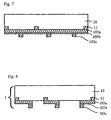
- a bump of electronic component chip 1 that is joined directly to surface wiring section 21 of connecting multi-layer substrate 2 can be also formed in the manner as shown in Figs. 6 to 8. That is, conductive layer 103a consisting of copper is formed on the surface of electronic component chip 1 including electrode 11 by utilizing an evaporation method or the like followed by forming etching stop layer 103b consisting of nickel thereon by utilizing a publicly known plating method, evaporation method or the like. And further thereon, conductive layer 103c consisting of copper is formed in the same manner as described for the etching stop layer 103b consisting of nickel.
- conductive layer 103a consisting of copper on the surface of electronic component chip 1 including electrode 11 and, by utilizing the joint technique of metal foils as disclosed in Domestic Re-publication of PCT patent Application WO 00/19533, the joint surfaces of a nickel foil material forming etching stop layer 103b and a copper foil material forming conductive layer 103c are previously subjected to an activation treatment in a vacuum chamber followed by laminating and cold welding the copper foil and nickel foil to form a cladding board.
- the nickel surface of the cladding board and the aforementioned conductive layer 103a surface provided on electronic component chip 1 are subjected to an activation treatment in a vacuum chamber followed by laminating and cold welding the cladding board and electronic component chip 1 to form three layers constituted of conductive layer 103a consisting of copper, etching stop layer 103b consisting of nickel and conductive layer 103c consisting of copper.
- a cladding material of three layers constituted of conductive layer 103a, etching stop layer 103b and conductive layer 103c may be formed, which is pressure-welded and laminated to the surface of electronic component chip 1 including electrode 11 by utilizing a pressure-welding method as disclosed in Domestic Re-publication of PCT patent Application WO 99/58470.
- the base may be formed by utilizing a conventional buildup method.
- it may be constituted by utilizing the joint technique of metal foils as disclosed in Domestic Re-publication of PCT patent Application WO 00/05934 and a selective etching method in the similar way to the case of electronic component chip 1 to form a base, providing an insulative layer and surface wiring section 21 on the base surface, then electrically connecting surface wiring section 21 and interior circuit section 22.
- surface wiring section 21 of connecting multi-layer substrate 2 is abutted directly and joined with bump 13 of electronic component chip 1 to give electronic circuit device 40.
- Fig. 10 is a schematic cross-sectional view of the electronic circuit device according to Claim 3 of the invention.
- electronic component chip 1 to which bump 13 is formed in the same manner as described in Embodiment 1 is joined directly with interposer 6.
- interposer 6 is constituted of a substrate 61 made of a heat-resistant resin to which surface wiring sections 62 being electrically connected with each other are formed.
- Surface wiring section 62 of one side of interposer 6 is abutted to bump 13 of electronic component chip 1, which are directly joined in the same manner as described in Embodiment 1 to constitute electronic component chip 7 with the interposer.
- connecting multi-layer substrate 2 is constituted in the same manner as shown in Fig. 9.
- Surface wiring section 21 of connecting multi-layer substrate 2 is abutted via solder ball 14 to surface wiring section 62 of the side to be joined with connecting multi-layer substrate 2 of interposer 6 of semiconductor chip 7 with the interposer constituted in the aforementioned manner, which are heated to a temperature capable of melting solder 14 and pressed to connect electrically surface wiring section 62 of the interposer with surface wiring section 21 of the connecting multi-layer substrate via solder ball 14.
- electronic circuit device 40 can be obtained.
- bump 13 is provided to electrode 11 of electronic component chip 1
- a bump may be provided to surface wiring section 62 of interposer 6; or bumps may be provided to both of electrode 11 and surface wiring section 62 of interposer 6.
- an example of the electronic circuit device in which the connecting multi-layer substrate is joined directly or via the interposer with the electronic component chip, is shown.
- an electronic circuit device that is constituted by joining respective electronic component chips (for example, a semiconductor chip and another semiconductor chip, a semiconductor chip and resistive element chip, etc.).
- respective electronic component chips for example, a semiconductor chip and another semiconductor chip, a semiconductor chip and resistive element chip, etc.
- an example of an electronic circuit device constituted by joining respective electronic component chips will be described.
- Fig. 11 is a schematic cross-sectional view of the electronic circuit device according to Claim 5 of the invention.
- the figure represents the case where respective electronic component chips are joined via an interposer.
- firstly bump 23a of electrode 11a of a first electronic component chip 1a to be one electronic component chip is abutted to surface wiring section 62a provided to one side of interposer 6, which are joined directly in the same manner as described in Embodiment 1.
- bump 23b of electrode 11b of a second electronic component chip 1b to be the other electronic component chip is abutted to surface wiring section 62b provided to the other side of interposer 6, which are joined directly in the same manner as described in Embodiment 1.
- bump 23a for joining is provided to electrode 11a of the first electronic component chip 1a
- the bump may be provided to surface wiring section 62a of interposer 6, or bumps may be provided to both of the first electronic component chip 1a and interposer 6.
- bump 23b for joining is provided to electrode 11b of the second electronic component chip 1b
- the bump may be provided to surface wiring section 62b of interposer 6, or bumps may be provided to both of the second electronic component chip 1b and interposer 6.
- bump 24 for joining is provided to connecting multi-layer substrate 15, the bump may be provided to electrode 11b of the second electronic component chip 1b or bumps may be provided to both of connecting multi-layer substrate 15 and second electronic component chip 1b.
- the figure of the bump formed in Embodiments 1 to 3 is preferably either a truncated cone or a truncated pyramid, and length A of the diameter of the top or the diagonal line of the top is 10 % or more of height H of the bump, as shown in Fig. 12.
- a small area of the top of the bump in this way results in a large loaded pressure per unit area at joining to improve stability of the joining.
- the invention intends an electronic circuit device being downsized at high density, and the height of the bump is 200 ⁇ m at the highest. Therefore it is difficult to make the length of the diameter of the top or the diagonal line of the top of the bump extremely small, and the lower limit of the length is 10 % of the height of the bump.
- the electronic component chip and connecting multi-layer substrate, or respective electronic component chips are joined directly and metallurgical with or without an interposer to give a stable electric connection.
- the figure of the bump is a truncated cone or a truncated pyramid having a length of the diameter of the top or the diagonal line of the top of 10 % or more of the height of the bump. A small area of the top of the bump in this way results in a large loaded pressure per unit area at joining to improve stability of the joining. Accordingly, the electronic circuit device according to the invention has an especially excellent actuation reliability.
Landscapes
- Engineering & Computer Science (AREA)
- Microelectronics & Electronic Packaging (AREA)
- Manufacturing & Machinery (AREA)
- Wire Bonding (AREA)
Abstract
An electronic circuit device capable of providing a stable
electrical connection between an electronic component chip and
a connecting multi-layer substrate, and being downsized at high
density; and a production method therefor. An electronic
component chip (1) and a connecting multi-layer substrate (2)
or electronic component chips are heated in an inactive
atmosphere such as argon or a reducing atmosphere such as
hydrogen and pressure-welded to each other with or without an
intermediary of an interposer (6), or their joint surfaces are
activated and then pressure-welded at room temperature or by
heating, thereby producing an electronic circuit device (40)
by directly and metallurgically joining them by using any one
of the above methods.
Description
- The present invention relates to an electronic circuit device, particularly to an electronic circuit device being downsized at high density and a production method thereof.
- In recent years, for a mobile phone, a digital video camera, a notebook-size computer and the like, augmented efforts are devoted to downsizing, thinning, lightening and cheapening for the purpose of improving further portability. Therefore, in an electronic circuit device used for these devices and mounted with chips of electronic components such as a semiconductor such as IC, a capacitor (condenser), a resistive element or an inductor on a multi-layer substrate, development studies are proceeded on how to connect electronic component chips to be mounted such as a semiconductor chip to a multi-layer substrate at high density, in addition to downsizing electronic component chips.
- As a result, a flip chip mounting method, in which an electronic component chip is directly connected in face down to be mounted on a multi-layer substrate, has been practiced as a mounting method realizing a high density. In the flip chip mounting, connecting electrodes provided to electronic component chips are connected to wiring sections provided on a multi-layer substrate in a block via an electrical connection member such as solder or gold.
- Fig. 3 shows a schematic cross-sectional view of an example of a connection system by the flip chip mounting method in a conventional electronic circuit device. As shown in Fig. 1,
electronic component chip 1 compriseselectronic component 10,electrode 11 provided on one side thereof andbump 12 consisting of gold or solder for connection formed onelectrode 11. As shown in Fig. 2, connectingmulti-layer substrate 2 is constituted ofmulti-layer metal board 3 provided withsurface wiring section 21 andinterior circuit section 22. Andbump 12 ofelectronic component chip 1 andsurface wiring section 21 of connectingmulti-layer substrate 2 are abutted viasolder ball 14, which are pressurized while heating to atemperature allowing solder 14 to melt to connect electricallyelectronic component chip 1 and connectingmulti-layer substrate 2 viaelectrode 11,bump 12,solder ball 14 andsurface wiring section 21 of the connecting multi-layer substrate. Subsequently, heat-curable sealing resin 5 is injected betweensolder balls 14 to be heated to cure. In this way,electronic circuit device 40 by the flip chip mounting method as shown in Fig. 3 can be obtained. - However, an electronic circuit device thus flip chip-mounted has such a disadvantage that stable electric connection can not be obtained between the electronic component chip and connecting multi-layer substrate, since a large difference between thermal expansions of curable resin and the bump constituted of a solder ball tends to generate warp during heating to cure the resin, or a crack tends to generate when it is subjected to a rapid temperature variation or mechanical shock to generate joint breakage.
- In the invention, it is an object to provide an electronic circuit device being downsized at high density that gives a stable electric connection between an electronic component chip such as a semiconductor chip and a multi-layer substrate, and a production method thereof.
- The electronic circuit device according to
Claim 1 of the invention is an electronic circuit device constituted by integrating: - an electronic component chip comprising an electronic component and a bump formed on an electrode of the electronic component; and
- a connecting multi-layer substrate comprising a multi-layer substrate and an interior circuit section and a surface wiring section formed for the multi-layer substrate and electrically connected with each other, by joining directly the bump formed on the electrode of the electronic component to the surface wiring section.
-
- In addition, the electronic circuit device according to
Claim 2 is an electronic circuit device constituted by integrating: - an electronic component chip; and
- a connecting multi-layer substrate comprising a multi-layer substrate, an interior circuit section and a surface wiring section formed for the multi-layer substrate and electrically connected with each other, and a bump formed on the surface wiring section, by joining directly an electrode of an electronic component to the bump formed on the surface wiring section.
-
- Further, the electronic circuit device according to
Claim 3 is an electronic circuit device constituted by integrating: - an electronic component chip with an interposer constituted of an electronic component chip comprising an electronic component and a bump formed on an electrode of the electronic component, and an interposer including surface wiring sections electrically connected with each other for a substrate, through joining directly the surface wiring section on one side of the substrate of the interposer to the bump formed on the electrode of the electronic component; and
- a connecting multi-layer substrate comprising a multi-layer substrate and an interior circuit section and surface wiring section formed for the multi-layer substrate and electrically connected with each other, by joining the surface wiring section of the interposer to the surface wiring section of the multi-layer substrate via a solder ball.
-
- Further, the electronic circuit device according to Claim 4 is an electronic circuit device constituted by integrating:
- an electronic component chip with an interposer constituted of an electronic component chip and an interposer comprising surface wiring sections electrically connected with each other for a substrate and a bump formed on the surface wiring section, through joining directly the bump formed on the surface wiring section of one side of the substrate of the interposer to an electrode of an electronic component; and
- a connecting multi-layer substrate comprising a multi-layer substrate and an interior circuit section and surface wiring section formed for the multi-layer substrate and electrically connected with each other, by joining the surface wiring section of the interposer to the surface wiring section of the multi-layer substrate via a solder ball.
-
- Further, the electronic circuit device according to
Claim 5 is an electronic circuit device constituted by integrating: - a first electronic component chip comprising a first electronic component and a bump formed on an electrode of the first electronic component;
- an interposer having surface wiring sections electrically connected with each other for a substrate; and
- a second electronic component chip comprising a second electronic component and a bump formed on an electrode of the second electronic component, by joining directly the bump on the electrode of the first electronic component to the surface wiring section of one side of the interposer, and the surface wiring section of the other side of the interposer to the bump on the electrode of the second electronic component, respectively.
-
- Further, the electronic circuit device according to
Claim 6 is an electronic circuit device constituted by integrating: - a first electronic component chip;
- an interposer comprising surface wiring sections electrically connected with each other for a substrate and a bump formed on the surface wiring section; and
- a second electronic component chip comprising a second electronic component and a bump formed on an electrode of the second electronic component, by joining directly the electrode of the first electronic component to the bump on the surface wiring section of one side of the interposer, and the surface wiring section of the other side of the interposer to the bump on the electrode of the second electronic component, respectively.
-
- Further, the electronic circuit device according to
Claim 7 is an electronic circuit device constituted by integrating: - a first electronic component chip;
- an interposer comprising surface wiring sections electrically connected with each other for a substrate and a bump formed on the surface wiring section; and
- a second electronic component chip, by joining directly an electrode of a first electronic component to the bump on the surface wiring section of one side of the interposer, and the bump on the surface wiring section of the other side of the interposer to an electrode of a second electronic component, respectively.
-
- In addition, an electronic circuit device according to any of
claims 1 to 7, characterized in that an electronic component is any of a semiconductor, a capacitor, a resistive element or an inductor; and further
an electronic circuit device according to any ofclaims 1 to 7, characterized in that a figure of the bump is a truncated cone or a truncated pyramid having a length of a diameter of the top or a diagonal line of the top of 10 % or more of the height of the bump. - The production method of an electronic circuit device according to
Claim 10 of the invention is a production method of an electronic circuit device characterized by integrating: - an electronic component chip comprising an electronic component and a bump formed on an electrode of the electronic component; and
- a connecting multi-layer substrate comprising a multi-layer substrate and an interior circuit section and surface wiring section formed for the multi-layer substrate and electrically connected with each other, by joining directly the bump formed on the electrode of the electronic component to the surface wiring section.
-
- In addition, the production method of an electronic circuit device according to
Claim 11 is a production method of an electronic circuit device characterized by integrating: - an electronic component chip; and
- a connecting multi-layer substrate comprising a multi-layer substrate, an interior circuit section and surface wiring section formed for the multi-layer substrate and electrically connected with each other, and a bump formed on the surface wiring section, by joining directly an electrode of an electronic component to the bump formed on the surface wiring section.
-
- Further, the production method of an electronic circuit device according to
Claim 12 is a production method of an electronic circuit device characterized by integrating: - an electronic component chip with an interposer constituted of an electronic component chip comprising an electronic component and a bump formed on an electrode of the electronic component and an interposer having a substrate with surface wiring sections electrically connected with each other, through joining directly the surface wiring section of one side of the substrate of the interposer to the bump formed on the electrode of the electronic component,
- by joining the surface wiring section of the interposer, via a solder ball, to a connecting multi-layer substrate comprising a multi-layer substrate and an interior circuit section and surface wiring section formed for the multi-layer substrate and electrically connected with each other.
-
- Further, the production method of an electronic circuit device according to
Claim 13 is a production method of an electronic circuit device characterized by integrating: - an electronic component chip with an interposer constituted of an electronic component chip and an interposer comprising surface wiring sections electrically connected with each other for a substrate and bumps formed on the surface wiring sections through joining directly the bump formed on the surface wiring section of one side of the substrate of the interposer to an electrode of an electronic component,
- by joining the surface wiring section of the interposer, via a solder ball, to a connecting multi-layer substrate comprising a multi-layer substrate and an interior circuit section and surface wiring section formed for the multi-layer substrate and electrically connected with each other.
-
- Further, the production method of an electronic circuit device according to
Claim 14 is a production method of an electronic circuit device characterized by integrating: - a first electronic component chip comprising a first electronic component and a bump formed on an electrode of the first electronic component;
- an interposer comprising surface wiring sections electrically connected with each other on both sides of a substrate; and
- a second electronic component chip comprising a second electronic component and a bump formed on an electrode of the second electronic component, by joining directly the bump on the electrode of the first electronic component to the surface wiring section of one side of the interposer, and the surface wiring section of the other side of the interposer to the bump on the electrode of the second electronic component, respectively.
-
- Further, the production method of an electronic circuit device according to
Claim 15 is a production method of an electronic circuit device characterized by integrating: - a first electronic component chip;
- an interposer comprising surface wiring sections electrically connected with each other for a substrate and a bump formed on the surface wiring section; and
- a second electronic component chip comprising a second electronic component and a bump formed on an electrode of the second electronic component, by joining directly an electrode of a first electronic component to the bump on one side of the surface wiring section of the interposer, and the surface wiring section of the other side of the interposer to the bump on the electrode of the second electronic component, respectively.
-
- Further, the production method of an electronic circuit device according to
Claim 16 is a production method of an electronic circuit device characterized by integrating: - a first electronic component chip;
- an interposer comprising surface wiring sections electrically connected with each other for a substrate and a bump formed on the surface wiring section; and
- a second electronic component chip, by joining directly an electrode of a first electronic component to the bump on the surface wiring section of one side of the interposer, and the bump on the surface wiring section of the other side of the interposer to an electrode of a second electronic component, respectively.
-
- In addition, the production method of an electronic circuit device according to any of
Claims 10 to 16, characterized in that the direct joining is carried out by heating in an inactive atmosphere or a reducing atmosphere to 200 to 300 °C and pressure-welding (Claim 17); or
by cold-rolling at ordinary temperatures after a previous activation treatment of the joint surfaces (Claim 18) . - And the production method of an electronic circuit device according to Claim 18 is characterized in that the activation treatment is carried out by irradiating any of plasma, ions or atoms in a vacuum chamber; or
the pressure-welding is carried out either at room temperature or by heating. -
- Fig. 1 is a schematic cross-sectional view illustrating an example of an electronic component chip to which a conventional bump is formed;
- Fig. 2 is a schematic cross-sectional view illustrating an example of a connecting multi-layer substrate;
- Fig. 3 is a schematic cross-sectional view illustrating an example of connection system of a conventional electronic circuit device;
- Fig. 4 is a schematic cross-sectional view illustrating an example of a state at one step of the production process of the electronic component chip according to the invention;
- Fig. 5 is a schematic cross-sectional view illustrating an example of the electronic component chip according to the invention;
- Fig. 6 is a schematic cross-sectional view illustrating an example of a state at one step of another production process of the electronic component chip according to the invention;
- Fig. 7 is a schematic cross-sectional view illustrating an example of a state at another step of another production process of the electronic component chip according to the invention;
- Fig. 8 is a schematic cross-sectional view illustrating another example of the electronic component chip according to the invention;
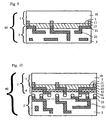
- Fig. 9 is a schematic cross-sectional view illustrating an example of the connection system of the electronic circuit device according to the invention;
- Fig. 10 is a schematic cross-sectional view illustrating another example of the connection system of the electronic circuit device according to the invention;
- Fig. 11 is a schematic cross-sectional view illustrating another example of the connection system of the electronic circuit device according to the invention; and
- Fig. 12 is a schematic cross-sectional view illustrating the cross-sectional figure of the bump of the electronic circuit device according to the invention.
-
- Hereinafter, the invention will be described in detail with reference to the drawings.
- Fig. 9 is a schematic cross-sectional view of the electronic circuit device according to
Claim 1 of the invention: In the figure, electronic component chip 1 (for example, a semiconductor chip) , which is a chip of any of a semiconductor, a capacitor, a resistive element or an inductor, comprises electronic component 10 (for example, a semiconductor, or any of following electronic components other than the semiconductor), which is any of a semiconductor, a capacitor, a resistive element or an inductor,electrode 11 provided on one side thereof and bump 13 formed onelectrode 11. Through joining directly this to surfacewiring section 21 of connectingmulti-layer substrate 2,electronic circuit device 40 is constituted.Bump 13 ofelectronic component chip 1 that is joined directly tosurface wiring section 21 of connectingmulti-layer substrate 2 can be formed by patterning with a resist so as to expose the part ofelectrode 11 alone, mounding a layer to bebump 13 onelectrode 11 by using an electrode plating method, and then removing the resist. Also, it can be formed in the manner as shown in Figs. 4 and 5. That is, by utilizing the method disclosed in Domestic Re-publication of PCT patent Application WO 99/58470 wherein surfaces to be adhered are subjected to an activation treatment and then the treated surfaces are pressure-welded, the surface ofelectronic component chip 1 includingelectrode 11 and the surface of copper foil to be adhered, which will constituteconductive layer 103, are subjected to an activation treatment followed by pressure-welding lamination to formconductive layer 103, subsequently bump 13 is formed onelectrode 11 by utilizing an etching method. - A bump of
electronic component chip 1 that is joined directly tosurface wiring section 21 of connectingmulti-layer substrate 2 can be also formed in the manner as shown in Figs. 6 to 8. That is,conductive layer 103a consisting of copper is formed on the surface ofelectronic component chip 1 includingelectrode 11 by utilizing an evaporation method or the like followed by formingetching stop layer 103b consisting of nickel thereon by utilizing a publicly known plating method, evaporation method or the like. And further thereon,conductive layer 103c consisting of copper is formed in the same manner as described for theetching stop layer 103b consisting of nickel. Alternatively, after formingconductive layer 103a consisting of copper on the surface ofelectronic component chip 1 includingelectrode 11 and, by utilizing the joint technique of metal foils as disclosed in Domestic Re-publication of PCT patent Application WO 00/19533, the joint surfaces of a nickel foil material formingetching stop layer 103b and a copper foil material formingconductive layer 103c are previously subjected to an activation treatment in a vacuum chamber followed by laminating and cold welding the copper foil and nickel foil to form a cladding board. Then, the nickel surface of the cladding board and the aforementionedconductive layer 103a surface provided onelectronic component chip 1 are subjected to an activation treatment in a vacuum chamber followed by laminating and cold welding the cladding board andelectronic component chip 1 to form three layers constituted ofconductive layer 103a consisting of copper,etching stop layer 103b consisting of nickel andconductive layer 103c consisting of copper. Alternatively, by utilizing the joint technique of metal foils as disclosed in Domestic Re-publication of PCT patent Application WO 00/19533, a cladding material of three layers constituted ofconductive layer 103a,etching stop layer 103b andconductive layer 103c may be formed, which is pressure-welded and laminated to the surface ofelectronic component chip 1 includingelectrode 11 by utilizing a pressure-welding method as disclosed in Domestic Re-publication of PCT patent Application WO 99/58470. - Through selectively etching the three layers thus obtained, it is also possible to form, to
electronic component chip 1, bump 103c electrically connected fromelectrode 11 viasurface wiring section 103a andnickel section 103b at a position dislocated fromelectrode 11. - On the other hand, regarding connecting
multi-layer substrate 2, the base may be formed by utilizing a conventional buildup method. Alternatively, it may be constituted by utilizing the joint technique of metal foils as disclosed in Domestic Re-publication of PCT patent Application WO 00/05934 and a selective etching method in the similar way to the case ofelectronic component chip 1 to form a base, providing an insulative layer andsurface wiring section 21 on the base surface, then electrically connectingsurface wiring section 21 andinterior circuit section 22. Subsequently, as shown in Fig. 9,surface wiring section 21 of connectingmulti-layer substrate 2 is abutted directly and joined withbump 13 ofelectronic component chip 1 to giveelectronic circuit device 40. - Regarding the joining method, they can be joined directly and metallurgically by utilizing either of the following methods:
- 1) pressure-welding is performed in an inactive atmosphere such as argon or in a reducing atmosphere such as hydrogen while heating to 200 to 300 °C; and
- 2) joint surfaces are activated previously by irradiating atoms
followed by pressure-welding at room temperature or while
heating to 200 to 300 °C. The activation treatment is possible
by irradiation of plasma or ions. However, since irradiation
of plasma or ions may charge members to destroy, atom
irradiation is preferred. Subsequently, sealing
resin 5 is filled aroundbump 13. In this connection, althoughbump 13 is provided to theelectrode 11 ofelectronic component chip 1 in the aforementioned constitution, the bump may be provided tosurface wiring section 21 of connectingmulti-layer substrate 2; or bumps may be provided to both ofelectrode 11 ofelectronic component chip 1 andsurface wiring section 21 of connectingmulti-layer substrate 2. -
- Fig. 10 is a schematic cross-sectional view of the electronic circuit device according to
Claim 3 of the invention. In this figure, firstly,electronic component chip 1 to which bump 13 is formed in the same manner as described inEmbodiment 1 is joined directly withinterposer 6. That is,interposer 6 is constituted of a substrate 61 made of a heat-resistant resin to which surface wiring sections 62 being electrically connected with each other are formed. Surface wiring section 62 of one side ofinterposer 6 is abutted to bump 13 ofelectronic component chip 1, which are directly joined in the same manner as described inEmbodiment 1 to constituteelectronic component chip 7 with the interposer. - On the other hand, connecting
multi-layer substrate 2 is constituted in the same manner as shown in Fig. 9.Surface wiring section 21 of connectingmulti-layer substrate 2 is abutted viasolder ball 14 to surface wiring section 62 of the side to be joined with connectingmulti-layer substrate 2 ofinterposer 6 ofsemiconductor chip 7 with the interposer constituted in the aforementioned manner, which are heated to a temperature capable of meltingsolder 14 and pressed to connect electrically surface wiring section 62 of the interposer withsurface wiring section 21 of the connecting multi-layer substrate viasolder ball 14. In this way,electronic circuit device 40 can be obtained. In this connection, in the aforementioned constitution, althoughbump 13 is provided to electrode 11 ofelectronic component chip 1, a bump may be provided to surface wiring section 62 ofinterposer 6; or bumps may be provided to both ofelectrode 11 and surface wiring section 62 ofinterposer 6. - In the aforementioned Embodiment, an example of the electronic circuit device, in which the connecting multi-layer substrate is joined directly or via the interposer with the electronic component chip, is shown. However, there may be such a case as an electronic circuit device that is constituted by joining respective electronic component chips (for example, a semiconductor chip and another semiconductor chip, a semiconductor chip and resistive element chip, etc.). Hereinafter, an example of an electronic circuit device constituted by joining respective electronic component chips will be described.
- Fig. 11 is a schematic cross-sectional view of the electronic circuit device according to
Claim 5 of the invention. The figure represents the case where respective electronic component chips are joined via an interposer. In this figure, firstly bump 23a of electrode 11a of a first electronic component chip 1a to be one electronic component chip is abutted tosurface wiring section 62a provided to one side ofinterposer 6, which are joined directly in the same manner as described inEmbodiment 1. Subsequently, bump 23b of electrode 11b of a second electronic component chip 1b to be the other electronic component chip is abutted tosurface wiring section 62b provided to the other side ofinterposer 6, which are joined directly in the same manner as described inEmbodiment 1. In this way, respective electronic component chips can be connected electrically via the interposer on both sides thereof. In addition, as shown in Fig. 11,surface wiring section 62b of one side ofinterposer 6 is abutted and joined withbump 24 provided to one side of connectingmulti-layer substrate 15 to connect electrically with connectingmulti-layer substrate 15. Subsequently, sealingresin 16 is injected between connectingmulti-layer substrate 15 and a second electronic component chip 1b and heated to cure. A surface wiring section (not shown) provided to the other side of connectingmulti-layer substrate 15 is provided withbump 17, which makes it possible to connect with another multi-layer substrate, electronic component chip or the like (not shown). In this way,electronic circuit device 40 which is constituted by joining respective electronic component chips can be obtained. - In this connection, although
bump 23a for joining is provided to electrode 11a of the first electronic component chip 1a, the bump may be provided tosurface wiring section 62a ofinterposer 6, or bumps may be provided to both of the first electronic component chip 1a andinterposer 6. Further, although bump 23b for joining is provided to electrode 11b of the second electronic component chip 1b, the bump may be provided tosurface wiring section 62b ofinterposer 6, or bumps may be provided to both of the second electronic component chip 1b andinterposer 6. Furthermore, althoughbump 24 for joining is provided to connectingmulti-layer substrate 15, the bump may be provided to electrode 11b of the second electronic component chip 1b or bumps may be provided to both of connectingmulti-layer substrate 15 and second electronic component chip 1b. - In the invention, the figure of the bump formed in
Embodiments 1 to 3 is preferably either a truncated cone or a truncated pyramid, and length A of the diameter of the top or the diagonal line of the top is 10 % or more of height H of the bump, as shown in Fig. 12. A small area of the top of the bump in this way results in a large loaded pressure per unit area at joining to improve stability of the joining. The invention intends an electronic circuit device being downsized at high density, and the height of the bump is 200 µm at the highest. Therefore it is difficult to make the length of the diameter of the top or the diagonal line of the top of the bump extremely small, and the lower limit of the length is 10 % of the height of the bump. - As shown in
Embodiments 1 to 3, in the electronic circuit device according to the invention, the electronic component chip and connecting multi-layer substrate, or respective electronic component chips are joined directly and metallurgical with or without an interposer to give a stable electric connection. Further, the figure of the bump is a truncated cone or a truncated pyramid having a length of the diameter of the top or the diagonal line of the top of 10 % or more of the height of the bump. A small area of the top of the bump in this way results in a large loaded pressure per unit area at joining to improve stability of the joining. Accordingly, the electronic circuit device according to the invention has an especially excellent actuation reliability.
Claims (20)
- An electronic circuit device constituted by integrating:by joining directly the bump formed on the electrode of the electronic component to the surface wiring section.an electronic component chip comprising an electronic component and a bump formed on an electrode of the electronic component; anda connecting multi-layer substrate comprising a multi-layer substrate and an interior circuit section and surface wiring section formed for the multi-layer substrate and electrically connected with each other,
- An electronic circuit device constituted by integrating:by joining directly an electrode of an electronic component to the bump formed on the surface wiring section.an electronic component chip; anda connecting multi-layer substrate comprising a multi-layer substrate, an interior circuit section and a surface wiring section formed for the multi-layer substrate and electrically connected with each other and a bump formed on the surface wiring section,
- An electronic circuit device constituted by integrating:by joining the surface wiring section of the interposer to the surface wiring section of the multi-layer substrate via a solder ball.an electronic component chip with an interposer constituted of an electronic component chip comprising an electronic component and a bump formed on an electrode of the electronic component, and an interposer including surface wiring sections electrically connected with each other for a substrate, through joining directly the surface wiring section on one side of the substrate of the interposer to the bump formed on the electrode of the electronic component; anda connecting multi-layer substrate comprising a multi-layer substrate and an interior circuit section and surface wiring section formed for the multi-layer substrate and electrically connected with each other,
- An electronic circuit device constituted by integrating:by joining the surface wiring section of the interposer to the surface wiring section of the multi-layer substrate via a solder ball.an electronic component chip with an interposer constituted of an electronic component chip and an interposer comprising surface wiring sections electrically connected with each other for a substrate and a bump formed on the surface wiring section, through joining directly the bump formed on the surface wiring section of one side of the substrate of the interposer to an electrode of an electronic component; anda connecting multi-layer substrate comprising a multi-layer substrate and an interior circuit section and surface wiring section formed for the multi-layer substrate and electrically connected with each other,
- An electronic circuit device constituted by integrating:by joining directly the bump on the electrode of the first electronic component to the surface wiring section of one side of the interposer, and the surface wiring section of the other side of the interposer to the bump on the electrode of the second electronic component, respectively.a first electronic component chip comprising a first electronic component and a bump formed on an electrode of the first electronic component;an interposer having surface wiring sections electrically connected with each other for a substrate; anda second electronic component chip comprising a second electronic component and a bump formed on an electrode of the second electronic component,
- An electronic circuit device constituted by integrating:by joining directly the electrode of the first electronic component to the bump on the surface wiring section of one side of the interposer, and the surface wiring section of the other side of the interposer to the bump on the electrode of the second electronic component, respectively.a first electronic component chip;an interposer comprising surface wiring sections electrically connected with each other for a substrate and a bump formed on the surface wiring section; anda second electronic component chip comprising a second electronic component and a bump formed on an electrode of the second electronic component,
- An electronic circuit device constituted by integrating:by joining directly an electrode of a first electronic component to the bump on the surface wiring section of one side of the interposer, and the bump on the surface wiring section of the other side of the interposer to an electrode of a second electronic component, respectively.a first electronic component chip;an interposer comprising surface wiring sections electrically connected with each other for a substrate and a bump formed on the surface wiring section; anda second electronic component chip,
- The electronic circuit device according to any of Claims 1 to 7, wherein the electronic component is any of a semiconductor, a capacitor, a resistive element or an inductance.
- The electronic circuit device according to any of Claims 1 to 7, characterized in that a figure of the bump is a truncated cone or a truncated pyramid having a length of a diameter of the top or a diagonal line of the top of 10 % or more of the height of the bump.
- A production method of an electronic circuit device characterized by integrating:by joining directly the bump formed on the electrode of the electronic component to the surface wiring section.an electronic component chip comprising an electronic component and a bump formed on an electrode of the electronic component; anda connecting multi-layer substrate comprising a multi-layer substrate and an interior circuit section and surface wiring section formed for the multi-layer substrate and electrically connected with each other,
- A production method of an electronic circuit device characterized by integrating:by joining directly an electrode of an electronic component to the bump formed on the surface wiring section.an electronic component chip; anda connecting multi-layer substrate comprising a multi-layer substrate, an interior circuit section and surface wiring section formed for the multi-layer substrate and electrically connected with each other, and a bump formed on the surface wiring section,
- A production method of an electronic circuit device characterized by integrating:an electronic component chip with an interposer constituted of an electronic component chip comprising an electronic component and a bump formed on an electrode of the electronic component and an interposer having a substrate with surface wiring sections electrically connected with each other, through joining directly the surface wiring section of one side of the substrate of the interposer to the bump formed on the electrode of the electronic component,by joining the surface wiring section of the interposer, via a solder ball, to a connecting multi-layer substrate comprising a multi-layer substrate and an interior circuit section and surface wiring section formed for the multi-layer substrate and electrically connected with each other.
- A production method of an electronic circuit device characterized by integrating:an electronic component chip with an interposer constituted of an electronic component chip and an interposer comprising surface wiring sections electrically connected with each other for a substrate and bumps formed on the surface wiring sections through joining directly the bump formed on the surface wiring section of one side of the substrate of the interposer to an electrode of an electronic component,by joining the surface wiring section of the interposer, via a solder ball, to a connecting multi-layer substrate comprising a multi-layer substrate and an interior circuit section and surface wiring section formed for the multi-layer substrate and electrically connected with each other.
- A production method of an electronic circuit device characterized by integrating:by joining directly the bump on the electrode of the first electronic component to the surface wiring section of one side of the interposer, and the surface wiring section of the other side of the interposer to the bump on the electrode of the second electronic component, respectively.a first electronic component chip comprising a first electronic component and a bump formed on an electrode of the first electronic component;an interposer comprising surface wiring sections electrically connected with each other for a substrate; anda second electronic component chip comprising a second electronic component and a bump formed on an electrode of the second electronic component,
- A production method of an electronic circuit device characterized by integrating:by joining directly an electrode of a first electronic component to the bump on one side of the surface wiring section of the interposer, and the surface wiring section of the other side of the interposer to the bump on the electrode of the second electronic component, respectively.a first electronic component chip;an interposer comprising surface wiring sections electrically connected with each other for a substrate and a bump formed on the surface wiring section; anda second electronic component chip comprising a second electronic component and a bump formed on an electrode of the second electronic component,
- A production method of an electronic circuit device characterized by integrating:by joining directly an electrode of a first electronic component to the bump on the surface wiring section of one side of the interposer, and the bump on the surface wiring section of the other side of the interposer to an electrode of a second electronic component, respectively.a first electronic component chip;an interposer comprising surface wiring sections electrically connected with each other for a substrate and a bump formed on the surface wiring section; anda second electronic component chip,
- The production method of an electronic circuit device according to any of Claims 10 to 16, characterized in that the direct joining is carried out by heating in an inactive atmosphere or a reducing atmosphere to 200 to 300 °C and pressure-welding.
- The production method of an electronic circuit device according to any of Claims 10 to 16, characterized in that the direct joining is carried out by pressure-welded after a previous activation treatment of the joint surfaces.
- The production method of an electronic circuit device according to Claim 18, characterized in that the activation treatment is carried out by irradiating any of plasma, ions or atoms in a vacuum chamber.
- The production method of an electronic circuit device according to Claim 18, characterized in that the pressure-welding is carried out either at room temperature or by heating.
Applications Claiming Priority (5)
| Application Number | Priority Date | Filing Date | Title |
|---|---|---|---|
| JP2002064666 | 2002-03-11 | ||
| JP2002064632 | 2002-03-11 | ||
| JP2002064666 | 2002-03-11 | ||
| JP2002064632 | 2002-03-11 | ||
| PCT/JP2003/002784 WO2003077307A1 (en) | 2002-03-11 | 2003-03-10 | Electronic circuit device and porduction method therefor |
Publications (1)
| Publication Number | Publication Date |
|---|---|
| EP1484793A1 true EP1484793A1 (en) | 2004-12-08 |
Family
ID=27806955
Family Applications (1)
| Application Number | Title | Priority Date | Filing Date |
|---|---|---|---|
| EP03744037A Withdrawn EP1484793A1 (en) | 2002-03-11 | 2003-03-10 | Electronic circuit device and porduction method therefor |
Country Status (7)
| Country | Link |
|---|---|
| US (1) | US20050082669A1 (en) |
| EP (1) | EP1484793A1 (en) |
| JP (1) | JPWO2003077307A1 (en) |
| KR (1) | KR20040086429A (en) |
| CN (1) | CN1639853A (en) |
| AU (1) | AU2003211879A1 (en) |
| WO (1) | WO2003077307A1 (en) |
Cited By (1)
| Publication number | Priority date | Publication date | Assignee | Title |
|---|---|---|---|---|
| WO2007148836A3 (en) * | 2006-06-22 | 2008-04-17 | Matsushita Electric Industrial Co Ltd | Electrode bonding method and part mounting apparatus |
Families Citing this family (11)
| Publication number | Priority date | Publication date | Assignee | Title |
|---|---|---|---|---|
| US7265446B2 (en) * | 2003-10-06 | 2007-09-04 | Elpida Memory, Inc. | Mounting structure for semiconductor parts and semiconductor device |
| JP2005340647A (en) * | 2004-05-28 | 2005-12-08 | Nec Compound Semiconductor Devices Ltd | Interposer substrate, semiconductor package, semiconductor device, and manufacturing method thereof |
| TW200721242A (en) * | 2005-07-25 | 2007-06-01 | Tokyo Electron Ltd | Method for processing metal member and apparatus for processing metal member |
| JP2007036571A (en) * | 2005-07-26 | 2007-02-08 | Shinko Electric Ind Co Ltd | Semiconductor device and manufacturing method thereof |
| US8350382B2 (en) * | 2007-09-21 | 2013-01-08 | Infineon Technologies Ag | Semiconductor device including electronic component coupled to a backside of a chip |
| US7927919B1 (en) * | 2009-12-03 | 2011-04-19 | Powertech Technology Inc. | Semiconductor packaging method to save interposer |
| US9554472B2 (en) * | 2013-12-19 | 2017-01-24 | Intel Corporation | Panel with releasable core |
| US9434135B2 (en) | 2013-12-19 | 2016-09-06 | Intel Corporation | Panel with releasable core |
| US9554468B2 (en) | 2013-12-19 | 2017-01-24 | Intel Corporation | Panel with releasable core |
| US9522514B2 (en) | 2013-12-19 | 2016-12-20 | Intel Corporation | Substrate or panel with releasable core |
| US10062494B2 (en) | 2014-11-03 | 2018-08-28 | Qorvo Us, Inc. | Apparatus with 3D inductors |
Family Cites Families (7)
| Publication number | Priority date | Publication date | Assignee | Title |
|---|---|---|---|---|
| JPH09181119A (en) * | 1995-12-27 | 1997-07-11 | Matsushita Electron Corp | Semiconductor device and manufacturing method thereof |
| JP3397045B2 (en) * | 1996-06-26 | 2003-04-14 | カシオ計算機株式会社 | Semiconductor device and manufacturing method thereof |
| JPH10135217A (en) * | 1996-10-29 | 1998-05-22 | Taiyo Yuden Co Ltd | Bump forming method |
| JP3853979B2 (en) * | 1998-06-16 | 2006-12-06 | 日東電工株式会社 | Manufacturing method of semiconductor devices |
| JP2001060602A (en) * | 1999-08-23 | 2001-03-06 | Fuji Electric Co Ltd | Flip chip mounting structure and manufacturing method thereof |
| JP2002064268A (en) * | 2000-08-18 | 2002-02-28 | Toray Eng Co Ltd | Mounting method and device |
| JP3874062B2 (en) * | 2000-09-05 | 2007-01-31 | セイコーエプソン株式会社 | Semiconductor device |
-
2003
- 2003-03-10 CN CNA038056089A patent/CN1639853A/en active Pending
- 2003-03-10 EP EP03744037A patent/EP1484793A1/en not_active Withdrawn
- 2003-03-10 US US10/504,426 patent/US20050082669A1/en not_active Abandoned
- 2003-03-10 KR KR10-2004-7013113A patent/KR20040086429A/en not_active Abandoned
- 2003-03-10 JP JP2003575417A patent/JPWO2003077307A1/en active Pending
- 2003-03-10 WO PCT/JP2003/002784 patent/WO2003077307A1/en not_active Ceased
- 2003-03-10 AU AU2003211879A patent/AU2003211879A1/en not_active Abandoned
Non-Patent Citations (1)
| Title |
|---|
| See references of WO03077307A1 * |
Cited By (2)
| Publication number | Priority date | Publication date | Assignee | Title |
|---|---|---|---|---|
| WO2007148836A3 (en) * | 2006-06-22 | 2008-04-17 | Matsushita Electric Industrial Co Ltd | Electrode bonding method and part mounting apparatus |
| US8449712B2 (en) | 2006-06-22 | 2013-05-28 | Panasonic Corporation | Electrode bonding method and part mounting apparatus |
Also Published As
| Publication number | Publication date |
|---|---|
| US20050082669A1 (en) | 2005-04-21 |
| CN1639853A (en) | 2005-07-13 |
| WO2003077307A1 (en) | 2003-09-18 |
| AU2003211879A1 (en) | 2003-09-22 |
| KR20040086429A (en) | 2004-10-08 |
| JPWO2003077307A1 (en) | 2005-07-07 |
Similar Documents
| Publication | Publication Date | Title |
|---|---|---|
| TW591765B (en) | Method of making electronic element-mounted substrate | |
| JP2500462B2 (en) | Inspection connector and manufacturing method thereof | |
| JP3709882B2 (en) | Circuit module and manufacturing method thereof | |
| JP4208631B2 (en) | Manufacturing method of semiconductor device | |
| US7234218B2 (en) | Method for separating electronic component from organic board | |
| JP2006520093A (en) | Manufacturing method of electronic module | |
| JP4537995B2 (en) | Method for manufacturing an electronic module | |
| EP1484793A1 (en) | Electronic circuit device and porduction method therefor | |
| CN100378968C (en) | electronic device | |
| WO2004112135A1 (en) | Substrate for semiconductor devices and semiconductor device | |
| JP2000100987A (en) | Multilayer circuit board for semiconductor chip module and method of manufacturing the same | |
| JP5110163B2 (en) | Manufacturing method of module with built-in components | |
| US6803253B2 (en) | Method for laminating and mounting semiconductor chip | |
| JP2001119147A (en) | Multilayer substrate with built-in electronic component and method of manufacturing the same | |
| US5303862A (en) | Single step electrical/mechanical connection process for connecting I/O pins and creating multilayer structures | |
| JP3269390B2 (en) | Semiconductor device | |
| CN100485895C (en) | Embedded chip package structure and process thereof | |
| JP2003298234A (en) | Multilayer wiring board, method for manufacturing the same, and wiring board | |
| US8334465B2 (en) | Wafer of circuit board and joining structure of wafer or circuit board | |
| JP2007306021A (en) | Electronic circuit device and manufacturing method thereof | |
| JP2004006705A (en) | Semiconductor device mounting structure and circuit board | |
| JP4023313B2 (en) | Multilayer semiconductor module and manufacturing method thereof | |
| KR100997880B1 (en) | Method of connecting and manufacturing a pad and a board of a chip embedded board and a multifunctional printed circuit board using the same | |
| JP2007035870A (en) | Semiconductor device | |
| JP2007096182A (en) | Printed wiring board, method for manufacturing the same, and electronic device incorporating the printed wiring board |
Legal Events
| Date | Code | Title | Description |
|---|---|---|---|
| PUAI | Public reference made under article 153(3) epc to a published international application that has entered the european phase |
Free format text: ORIGINAL CODE: 0009012 |
|
| 17P | Request for examination filed |
Effective date: 20040819 |
|
| AK | Designated contracting states |
Kind code of ref document: A1 Designated state(s): AT BE BG CH CY CZ DE DK EE ES FI FR GB GR HU IE IT LI LU MC NL PT RO SE SI SK TR |
|
| AX | Request for extension of the european patent |
Extension state: AL LT LV MK |
|
| STAA | Information on the status of an ep patent application or granted ep patent |
Free format text: STATUS: THE APPLICATION HAS BEEN WITHDRAWN |
|
| 18W | Application withdrawn |
Effective date: 20080226 |