EP1484766A1 - Magnetic storage unit using ferromagnetic tunnel junction element - Google Patents
Magnetic storage unit using ferromagnetic tunnel junction element Download PDFInfo
- Publication number
- EP1484766A1 EP1484766A1 EP03706934A EP03706934A EP1484766A1 EP 1484766 A1 EP1484766 A1 EP 1484766A1 EP 03706934 A EP03706934 A EP 03706934A EP 03706934 A EP03706934 A EP 03706934A EP 1484766 A1 EP1484766 A1 EP 1484766A1
- Authority
- EP
- European Patent Office
- Prior art keywords
- tunnel junction
- ferromagnetic tunnel
- word line
- magnetic force
- junction device
- Prior art date
- Legal status (The legal status is an assumption and is not a legal conclusion. Google has not performed a legal analysis and makes no representation as to the accuracy of the status listed.)
- Granted
Links
- 230000005291 magnetic effect Effects 0.000 title claims abstract description 127
- 230000005294 ferromagnetic effect Effects 0.000 title claims abstract description 99
- 230000005415 magnetization Effects 0.000 claims abstract description 111
- 230000004888 barrier function Effects 0.000 claims abstract description 7
- 238000010030 laminating Methods 0.000 abstract description 3
- 239000004065 semiconductor Substances 0.000 description 12
- 239000000758 substrate Substances 0.000 description 12
- 230000001965 increasing effect Effects 0.000 description 8
- 230000002093 peripheral effect Effects 0.000 description 8
- 239000010409 thin film Substances 0.000 description 6
- 230000009471 action Effects 0.000 description 3
- 238000007796 conventional method Methods 0.000 description 2
- 238000005516 engineering process Methods 0.000 description 2
- 230000002708 enhancing effect Effects 0.000 description 2
- 239000003302 ferromagnetic material Substances 0.000 description 2
- 230000006870 function Effects 0.000 description 2
- 238000009413 insulation Methods 0.000 description 2
- 239000002184 metal Substances 0.000 description 2
- 229910052751 metal Inorganic materials 0.000 description 2
- 229910003321 CoFe Inorganic materials 0.000 description 1
- 229910001030 Iron–nickel alloy Inorganic materials 0.000 description 1
- PNEYBMLMFCGWSK-UHFFFAOYSA-N aluminium oxide Inorganic materials [O-2].[O-2].[O-2].[Al+3].[Al+3] PNEYBMLMFCGWSK-UHFFFAOYSA-N 0.000 description 1
- 230000008859 change Effects 0.000 description 1
- 229910052593 corundum Inorganic materials 0.000 description 1
- 229910003460 diamond Inorganic materials 0.000 description 1
- 239000010432 diamond Substances 0.000 description 1
- 230000000694 effects Effects 0.000 description 1
- 239000012774 insulation material Substances 0.000 description 1
- 238000003475 lamination Methods 0.000 description 1
- 150000002739 metals Chemical class 0.000 description 1
- 239000002674 ointment Substances 0.000 description 1
- 229910001845 yogo sapphire Inorganic materials 0.000 description 1
Images


Classifications
-
- G—PHYSICS
- G11—INFORMATION STORAGE
- G11C—STATIC STORES
- G11C11/00—Digital stores characterised by the use of particular electric or magnetic storage elements; Storage elements therefor
- G11C11/02—Digital stores characterised by the use of particular electric or magnetic storage elements; Storage elements therefor using magnetic elements
- G11C11/14—Digital stores characterised by the use of particular electric or magnetic storage elements; Storage elements therefor using magnetic elements using thin-film elements
-
- G—PHYSICS
- G11—INFORMATION STORAGE
- G11C—STATIC STORES
- G11C11/00—Digital stores characterised by the use of particular electric or magnetic storage elements; Storage elements therefor
- G11C11/02—Digital stores characterised by the use of particular electric or magnetic storage elements; Storage elements therefor using magnetic elements
- G11C11/16—Digital stores characterised by the use of particular electric or magnetic storage elements; Storage elements therefor using magnetic elements using elements in which the storage effect is based on magnetic spin effect
-
- G—PHYSICS
- G11—INFORMATION STORAGE
- G11C—STATIC STORES
- G11C11/00—Digital stores characterised by the use of particular electric or magnetic storage elements; Storage elements therefor
- G11C11/02—Digital stores characterised by the use of particular electric or magnetic storage elements; Storage elements therefor using magnetic elements
- G11C11/14—Digital stores characterised by the use of particular electric or magnetic storage elements; Storage elements therefor using magnetic elements using thin-film elements
- G11C11/15—Digital stores characterised by the use of particular electric or magnetic storage elements; Storage elements therefor using magnetic elements using thin-film elements using multiple magnetic layers
-
- H—ELECTRICITY
- H01—ELECTRIC ELEMENTS
- H01L—SEMICONDUCTOR DEVICES NOT COVERED BY CLASS H10
- H01L27/00—Devices consisting of a plurality of semiconductor or other solid-state components formed in or on a common substrate
- H01L27/02—Devices consisting of a plurality of semiconductor or other solid-state components formed in or on a common substrate including semiconductor components specially adapted for rectifying, oscillating, amplifying or switching and having potential barriers; including integrated passive circuit elements having potential barriers
- H01L27/04—Devices consisting of a plurality of semiconductor or other solid-state components formed in or on a common substrate including semiconductor components specially adapted for rectifying, oscillating, amplifying or switching and having potential barriers; including integrated passive circuit elements having potential barriers the substrate being a semiconductor body
- H01L27/10—Devices consisting of a plurality of semiconductor or other solid-state components formed in or on a common substrate including semiconductor components specially adapted for rectifying, oscillating, amplifying or switching and having potential barriers; including integrated passive circuit elements having potential barriers the substrate being a semiconductor body including a plurality of individual components in a repetitive configuration
- H01L27/105—Devices consisting of a plurality of semiconductor or other solid-state components formed in or on a common substrate including semiconductor components specially adapted for rectifying, oscillating, amplifying or switching and having potential barriers; including integrated passive circuit elements having potential barriers the substrate being a semiconductor body including a plurality of individual components in a repetitive configuration including field-effect components
Definitions
- the present invention relates to a magnetic storage apparatus using ferromagnetic tunnel junction devices.
- Such ferromagnetic tunnel junction device is constituted by laminating a pair of ferromagnetic thin films on both top and back surfaces of an insulation thin film.
- One of the ferromagnetic thin films is called a fixed magnetization layer because it is always magnetized in a fixed direction.
- the other ferromagnetic thin film is called as a free magnetization layer because it is magnetized in the same direction (parallel direction) as the magnetization direction of the fixed magnetization layer or it is inverted in the opposite direction (anti-parallel direction) depending on a memory state of the ferromagnetic tunnel junction device.
- the insulation is called a tunnel barrier layer because it causes a tunnel current when voltage is applied between the fixed magnetization layer and the free magnetization layer.
- the ferromagnetic tunnel junction device has a structure which stably holds two states of different magnetization direction, that is, the state in which the free magnetization layer is magnetized in the same direction as that of the fixed magnetization layer or the state in which it is magnetized in the opposite magnetization direction to that of the fixed magnetization layer by the action of the magnetic force of the fixed magnetization layer, thereby storing the two states of different magnetization direction.
- these two different states of magnetization direction as two different memory states, that is, "0" and "1", it is possible to store two different memory states.
- the ferromagnetic tunnel junction device is capable of externally writing two different memory states externally by magnetizing the free magnetization layer in the same magnetization direction as or opposite magnetization direction to that of the fixed magnetization layer. It is to be noted that the memory states which are written in the ferromagnetic tunnel junction device can be read out by utilizing the giant magnetoresistance effect in which conductance in the tunnel barrier layer differs depending on the magnetization direction of the free magnetization layer.
- the magnetic storage apparatus utilizing the ferromagnetic tunnel junction devices is formed with a plurality of first wiring lines on a semiconductor substrate in the magnetization direction of the fixed magnetization layers of the ferromagnetic tunnel junction devices, a plurality of second wiring lines on the semiconductor substrate in the orthogonal direction to the magnetization direction of the fixed magnetization layers of the ferromagnetic tunnel junction devices.
- the ferromagnetic tunnel junction devices are disposed at cross points of the first wiring and the second wiring, which are formed in a lattice-like pattern.
- the first wiring is called a word line while the second wiring is called a bit line.
- a current is caused to flow through the word line so as to generate a word line magnetic force in the orthogonal direction to the direction of the current flow and also a current is caused to flow through the bit line so as to generate a bit line magnetic force in the orthogonal direction to the direction of the current flow.
- a combined magnetic force of the word line magnetic force and the bit line magnetic force acts upon the free magnetization layer, the free magnetization layer is then magnetized in the same direction as or opposite direction to the magnetization direction of the fixed magnetization layer.
- either one of the two states of magnetization direction generates in the free magnetization layer.
- Such state of magnetization direction is stably held by the action of the magnetic force of the fixed magnetization layer, thereby performing the storage operation in the ferromagnetic tunnel junction device.
- the current flowing through the word line is maintained always in the fixed direction so as to generate the word line magnetic force always in the fixed direction, and under this condition, only the bit line magnetic force is inverted by inverting the direction of current flowing through the bit line, thereby changing the magnetization direction of the combined magnetic force of the word line magnetic force and the bit line magnetic force.
- the magnetization direction of the free magnetization layer is inverted, thereby writing a desired memory state in the ferromagnetic tunnel junction device.
- the direction of the current flowing through the bit line is inverted while the direction of the current flowing through the word line remains always in the fixed direction, so that the current flows through the word line always in the fixed direction at the time of writing in the ferromagnetic tunnel junction device and, therefore, a constant potential difference is always generated between the word line and the peripheral area of the semiconductor substrate.
- a possible solution to prevent such electromigration from occurring is to improve resistance to electromigration of the word lines by increasing the width of the word lines, however, which accompanies another problem of increasing the size of the magnetic storage apparatus due to the increased width of the word lines.
- an object of the present invention is to provide a magnetic storage apparatus with improved resistance to electromigration of the word lines without increasing the width of the word lines.
- the magnetic storage apparatus using ferromagnetic tunnel junction devices is configured by forming the ferromagnetic tunnel junction device by laminating a fixed magnetization layer and a free magnetization layer by way of a tunnel barrier layer, disposing word lines in the magnetization direction of the fixed magnetization layer of the ferromagnetic tunnel junction devices, and disposing bit lines in orthogonal direction to the magnetization direction of the fixed magnetization layer of the ferromagnetic tunnel junction devices, in such a manner to write two different memory states in the ferromagnetic tunnel junction devices by inverting the current flowing through the bit lines, wherein the direction of the current flowing through the word lines is inverted in the same direction as or the opposite direction to the magnetization direction of the fixed magnetization layer, at the time of writing in the ferromagnetic tunnel junction devices.
- Inversion of the current flowing through the word lines is performed at every time of writing in the ferromagnetic tunnel junction devices.
- the direction of the current flowing through the word lines is not always fixed but inverted with time, thereby changing the current flowing through the word lines to a quasi-alternating current.
- the potential difference, which generates between the word line and the peripheral semiconductor substrate, is reversed with time, thereby preventing electromigration due to always constant potential difference from occurring, improving resistance to electromigration without increasing the width of the word lines that increases the size of the magnetic storage apparatus, and extending the lifetime by preventing troubles of the magnetic storage apparatus.
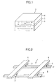
- the magnetic storage apparatus 1 uses ferromagnetic tunnel junction devices 2 as storage elements each of which stores two different memory states, for example, either "0" or "1".
- the ferromagnetic tunnel junction device 2 is made of a lamination in which a thin film fixed magnetization layer 3 and a thin film free magnetization layer 4 are laminated on a top and back surfaces of a tunnel barrier layer 5.
- the fixed magnetization layer 3 is made of a ferromagnetic material (for example, CoFe) and is magnetized always in a fixed direction.
- the free magnetization layer 4 is made of a ferromagnetic material (for example, NiFe) and magnetized in the same direction (parallel direction) as the magnetization direction of the fixed magnetization layer 3 or an opposite direction (anti-parallel direction).
- the tunnel barrier layer 5 is made of an insulation material (for example, Al 2 O 3 ).
- a plurality of word lines 7 is formed on a semiconductor substrate 6 in the direction of the magnetization direction of the fixed magnetization layer 3 of the ferromagnetic tunnel junction device 2 while a plurality of bit lines 8 is formed on the semiconductor substrate 6 in the orthogonal direction to the magnetization direction of the fixed magnetization layer 3 of the ferromagnetic tunnel junction device 2, and then, a plurality of ferromagnetic tunnel junction devices 2 disposed at cross points of the word lines 7 and the bit lines 8 which are formed in a lattice-like pattern. It is to be noted that only structure of the magnetic storage apparatus 1 necessary for writing the memory states in the ferromagnetic tunnel junction device 2 is described in the description and the structure for reading out the stored state written in the ferromagnetic tunnel junction device 2 is abbreviated.
- Writing either "0" or “1” memory state in the ferromagnetic tunnel junction device 2 is, in other words, magnetizing the free magnetization layer 4 in the same direction as or opposite direction to the magnetization direction of the fixed magnetization layer 3.
- magnetization of the free magnetization layer 4 of the ferromagnetic tunnel junction device 2 is carried out by a combined magnetic force 11 of a word line magnetic force 9 generated by applying a current to the word line 7 and a bit line magnetic force 10 generated by applying a current to the bit line 8 so as to act upon the free magnetization layer 4.
- the word line magnetic force 9 is generated in the orthogonal direction to the word line 7 of the ferromagnetic tunnel junction device 2, which is the direction from the near side to the far side in the drawing.
- the bit line magnetic force 10 is generated from the left to right direction, which is the orthogonal direction to the direction of the current flowing through the bit line 8. Accordingly, as shown in FIG. 3, the combined magnetic force 11 diagonally toward the far right side, which is constituted of the word line magnetic force 9 and the bit line magnetic force 10 , acts upon the free magnetization layer 4.
- Such combined magnetic force 11 is stably held inside the free magnetization layer 4 as a magnetic force 13, which is in the same direction as the magnetization direction of the fixed magnetization layer 3, by a magnetic force 12 in the fixed magnetization layer 3.
- the ferromagnetic tunnel junction device 2 is considered to store the memory state "0".
- FIG. 4 is an illustration of the memory state.
- the illustration of the memory state illustrates that the memory state will be either "0" or "1" depending on the direction of the combined magnetic force 11 of the word line magnetic force 9 and the bit line magnetic force 10.
- a horizontal axis represents the magnitude of the word line magnetic force 9 and a leftward current flow from the right to left through the word line 7 is defined as a positive direction.
- a vertical axis represents the magnitude of the bit line magnetic force 10 and a coming current flow from the far side to the near side through the bit line 8 is defined as a positive direction.
- the memory state is "0" if the combined magnetic force 11 is directed upwardly with respect to the horizontal axis, while the memory state is "1” if the combined magnetic force 11 is directed downwardly with respect to the horizontal axis.
- a substantially diamond shaped area surrounded by 4 arcs near the center portion in the illustration of the memory state is a non-inverting area. If the combined magnetic force 11 remains within the non-inverting area, the combined magnetic force 11 is too weak to magnetize the free magnetization layer 4 effectively.
- the magnetization direction of the word line magnetic force 9 is positive.
- the magnetization direction of the bit line magnetic force 10 is positive. Since the positive word line magnetic force 9 and the positive bit line magnetic force 10 make the direction of the combined magnetic force 11 upwardly, the memory state in the ferromagnetic tunnel junction device 2 is "0".
- the combined magnetic force 11 in the down rightward direction may be generated by the word line magnetic force 9 in the positive direction and the bit line magnetic force 10 in the negative direction as shown in FIG. 6, or alternatively, the case in which the combined magnetic force 11 in the down leftward direction may be generated by the word line magnetic force 9 in the negative direction and the bit line magnetic force 10 in the negative direction as shown in FIG. 7.
- the combined magnetic force 11 in the upper rightward direction is generated by the word line magnetic force 9 in the positive direction and the bit line magnetic force 10 in the positive direction as shown in FIG. 4, while in case of storing the memory state "1" in the ferromagnetic tunnel junction device 2, the combined magnetic force 11 in the down rightward direction is generatedby the word line magnetic force 9 in the positive direction and the bit line magnetic force 10 in the negative direction as shown in FIG. 6.
- the direction of the current flowing through the word line 7 at the time of writing the ferromagnetic tunnel junction device 2 is inverted in the same direction as the magnetization direction of the fixed magnetization layer 3 or inverted in the opposite direction thereto.
- the combined magnetic force 11 in the upper rightward direction is generated by the word line magnetic force 9 in the positive direction and the bit line magnetic force 10 in the positive direction as shown in FIG. 4.
- the combined magnetic force 11 in the down leftward direction is generated by the word line magnetic force 9 in the negative direction and the bit line magnetic force 10 in the negative direction as shown in FIG. 7.
- the way of inverting the direction of the current flowing through the word line 7 in the same direction as or opposite direction to the magnetization direction of the fixed magnetization layer 3 at the time of writing in the ferromagnetic tunnel junction device 2 does not to be limited to the above combination (the combination of the conditions as shown in FIG. 4 and FIG. 7).
- it may be generated the combined magnetic force 11 in the upper leftward direction by the word line magnetic force 9 in the negative direction and the bit line magnetic force 10 in the positive direction as shown in FIG.
- the invention does not to be limited to such example and it may be possible to invert the direction of the current flowing through the word line 7 at every time of writing in the ferromagnetic tunnel junction device 2.
- the combined magnetic force 11 in the upper rightward direction is generated by the word line magnetic force 9 in the positive direction and the bit line magnetic force 10 in the positive direction as shown in FIG. 4.
- the combined magnetic force 11 in the upper leftward direction is generatedbythe word line magnetic force 9 in the negative direction and the bit line magnetic force 10 in the positive direction as shown in FIG. 5.
- the combined magnetic force 11 in the upper rightward direction may be generated again by the word line magnetic force 9 in the positive direction and the bit linemagnetic force 10 in the positive direction as shown in FIG. 4.
- the above may be the similar in case of continuously storing the memory state "1" in the ferromagnetic tunnel junction device 7.
- the combined magnetic force 11 in the down rightward direction is generated by the word line magnetic force 9 in the positive direction and the bit line magnetic force 10 in the negative direction as shown in FIG. 6.
- the combined magnetic force 11 in the down leftward direction is generated by the word line magnetic force 9 in the negative direction and the bit line magnetic force 10 in the negative direction as shown in FIG. 7.
- the combined magnetic force 11 in the down rightward direction is again generated by the word line magnetic force 9 in the positive direction and the bit line magnetic force 10 in the negative direction as shown in FIG. 6.
- the direction of the current flowing through the word line 7 is not always fixed but is inverted with time, thereby changing the current flowing through the word line 7 into a quasi-alternating current. Accordingly, the potential difference generated between the word line 7 and the peripheral semiconductor substrate 6 is inverted with time, thereby effectively preventing the electromigration generation due to the constant potential difference generation. As a result, it is possible to improve resistance to electromigration without increasing the width of word lines 7, which increases the size of the magnetic storage apparatus 1, and to extend the lifetime of the magnetic storage apparatus 1 by preventing troubles in the magnetic storage apparatus 1.
- the left end of the word line 7 is coupled to a P type FET 14 which is connected to a power supply VDD and to an N type FET 15 which is connected to the ground GND while the right end of the word line 7 is coupled to a P type FET 16 which is connected to the power supply VDD and to an N type FET 17 which is connected to the ground GND.
- a back end of the bit line 8 is coupled to a P type FET 18 which is connected to the power supply VDD and to an N type FET 19 which is connected to the ground GND while a front end of the bit line 8 is coupled to a P type FET 20 which is connected to the power supply VDD and to an N type FET 21 which is connected to the ground GND.
- the device electrodes 22, 24, 26, 28 of these P type FETs 14, 16, 18, 20 and the device electrodes 23, 25, 27, 29 of these N type FETs 15, 17, 19, 21 are connected to a control circuit 30 so that the P type FETs 14, 16, 18, 20 and the N type FETs 15, 17, 19, 21 function as switching transistors.
- control signals 31 - 38 are inputted to the device electrodes 22 - 29 from the control circuit 30 for selectively switching the P type FETs 14, 16, 18, 20 and the N type FETs 15, 17, 19, 21, thereby inverting the direction of the currents flowing through the word line 7 and the bit line 8.
- the left end of the word line 7 is connected to the. ground GND while the right end of the word line 7 is connected to the power supply VDD, thereby causing the current through the word line 7 to flow left from the right end to the left end.
- control signals 35, 38 is inputted to the device electrode 26 of the P type FET 18 and to the device electrode 29 of the N type FET 21 for turning on the P type FET 18 and the N type FET 21 while the control signals 36, 37 is inputted to the device electrode 27 of the N type FET 19 and to the device electrode 28 of the P type FET 20 for turning off the N type FET 19 and the P type FET 20, thereby connecting the upper end of the bit line 8 to the power supply VDD and connecting the lower end of the bit line 8 to the ground GND and causing the current to flow downwardly through the bit line 8 from the upper end to the lower end.
- the control circuit 30 when the P type FET 18 and the N type FET 21 are turned off and the N type FET 19 while the P type FET 20 are turned on, the upper end of the bit line 8 is connected to the ground GND while the lower end of the bit line 8 is connected to the power supply VDD, thereby causing the current to flow upwardly through the bit line 8 from the lower end to the upper end.
- the control circuit 30 is a circuit for inverting the direction of the currents flowing through the bit line 8 and the word line 7 depending on whether the memory state which is stored in the ferromagnetic tunnel junction device 2 is "0" or "1".
- address decode signals 43, 44 are generated by decoding a row address signal 39 and a column address signal 40 which represent storage locations of the ferromagnetic tunnel junction devices 2 by a row address decoder 41 and a column address decoder 42, respectively.
- a true signal 48 which represents the input data 45 itself and a false signal 49 which is inversion of the input data 45 are generated by using a pair of inverter devices 46, 47 from the input data 45 to be stored in the ferromagnetic tunnel junction devices 2.
- the control signals 31 - 38 are generated from combinations of the address decode signals 43, 44, the true signal 48 and the false signal 49 by using NAND devices 50 - 53 and AND devices 54 - 57.
- represented by 58 is a write enable signal.
- a particular ferromagnetic tunnel junction device 2 is designated by the row address signal 39 and the column address signal 40.
- the write enable signal 58 becomes active (referred to as “1” herein)
- the address decode signals 43, 44 become active (referred to as “1” herein) by the row address decoder 41 and the column address decoder 42.
- the true signal 48 is also “0” by means of the two inverter devices 46, 47 while the false signal 49 is “1” by means of the inverter device 46.
- the control signal 31 is “1” by means of a NAND device 50, thereby turning off the P type FET 14.
- the control signal 32 is “1” by means of a -AND device 54, thereby turning on the N type FET 15, while the control signal 33 is “0” by means of a NAND device 51, thereby turning on the P type FET 16.
- the control signal 34 is “0” by means of an AND device 55, thereby turning off the N type FET 17.
- the left end of the word line 7 is connected to the ground GND while the right end of the word line 7 is connected to the power supply VDD, thereby causing the current to flow leftward through the word line 7 from the right end to the left end.
- the current flowing through the bit line 8 is controlled in the similar manner as the above.
- FIG. 10 The above operation of the circuit as shown and described by reference to FIG. 9 is shown in a timing chart in FIG. 10. It is shown in FIG. 10 that the leftward current flow through the word line 7 is "0”, the rightward current flow through the word line 7 is “1”, the forward current flow through the bit line 8 is "0" and the backward current flow through the bit line 8 is "1".
- the direction of the current flowing through not only the word line 7 but also the bit line 8 is inverted depending on whether the memory state which is to be stored in the ferromagnetic tunnel junction device 2 is "0" or "1".
- the direction of the current flowing through the word line 7 can be inverted at every time of writing in the ferromagnetic tunnel junction device 2, the direction of the current flowing through the word line 7 can be inverted after plural times of continuous writing, the direction of the current flowing through the word line 7 can be inverted at every designated time, or further the direction of the current flowing through the word line 7 can be inverted even in a single writing.
- the direction of the current flowing through the word line is inverted in the same direction as or opposite direction to the magnetization direction of the fixed magnetization layer at the time of writing in the ferromagnetic tunnel junction device, the direction of the current flowing through the word line is not always fixed but inverted with time, thereby making the current flowing through the word line quasi-alternating and inverting the potential difference with time, which is generated between the word line and the peripheral semiconductor substrate.
- electromigration due to generation of the constant potential difference is prevented and thus resistance to electromigration is improved without increasing the width of the word lines and increasing the size of the magnetic storage apparatus, and therefore, the lifetime of the magnetic storage apparatus is extended by preventing troubles therein.
Landscapes
- Engineering & Computer Science (AREA)
- Computer Hardware Design (AREA)
- Power Engineering (AREA)
- Physics & Mathematics (AREA)
- Condensed Matter Physics & Semiconductors (AREA)
- General Physics & Mathematics (AREA)
- Microelectronics & Electronic Packaging (AREA)
- Hall/Mr Elements (AREA)
- Mram Or Spin Memory Techniques (AREA)
- Semiconductor Memories (AREA)
Abstract
Description
Claims (2)
- A magnetic storage apparatus using a ferromagnetic tunnel junction device, comprising:a ferromagnetic tunnel junction device configured with
a fixed magnetization layer,
a free magnetization layer, and
a tunnel barrier layer disposed between said fixed magnetization layer and said free magnetization layer;a word line wired in a magnetization direction of said fixed magnetization layer of said ferromagnetic tunnel junction device;a bit line wired in an orthogonal direction to said magnetization direction of said fixed magnetization layer of said ferromagnetic tunnel junction device;writing means for writing two different memory states in said ferromagnetic tunnel junction device by inverting a current flowing through said bit line; andinverting means for inverting a direction of current flowing through said word line in a same direction as or an opposite direction to said magnetization direction of said fixed magnetization layer at the time of writing in said ferromagnetic tunnel junction device. - The magnetic storage apparatus using said ferromagnetic tunnel junction device according to claim 1, said inverting means for inverting said direction of current flowing through said word line inverts said direction of current flowing through said word line at every time of writing in said ferromagnetic tunnel junction device.
Applications Claiming Priority (3)
| Application Number | Priority Date | Filing Date | Title |
|---|---|---|---|
| JP2002031986 | 2002-02-08 | ||
| JP2002031986A JP3778100B2 (en) | 2002-02-08 | 2002-02-08 | Magnetic memory device using ferromagnetic tunnel junction element |
| PCT/JP2003/001348 WO2003067601A1 (en) | 2002-02-08 | 2003-02-07 | Magnetic storage unit using ferromagnetic tunnel junction element |
Publications (3)
| Publication Number | Publication Date |
|---|---|
| EP1484766A1 true EP1484766A1 (en) | 2004-12-08 |
| EP1484766A4 EP1484766A4 (en) | 2008-12-10 |
| EP1484766B1 EP1484766B1 (en) | 2011-06-01 |
Family
ID=27677951
Family Applications (1)
| Application Number | Title | Priority Date | Filing Date |
|---|---|---|---|
| EP03706934A Expired - Lifetime EP1484766B1 (en) | 2002-02-08 | 2003-02-07 | Magnetic storage unit using ferromagnetic tunnel junction element |
Country Status (6)
| Country | Link |
|---|---|
| US (1) | US7020010B2 (en) |
| EP (1) | EP1484766B1 (en) |
| JP (1) | JP3778100B2 (en) |
| KR (1) | KR100951189B1 (en) |
| CN (1) | CN1714402B (en) |
| WO (1) | WO2003067601A1 (en) |
Cited By (2)
| Publication number | Priority date | Publication date | Assignee | Title |
|---|---|---|---|---|
| DE102004047411B3 (en) * | 2004-09-28 | 2006-05-11 | Funktionale Materialien Rostock E.V. | Magnetic storage layer system |
| EP2369455B1 (en) * | 2010-03-23 | 2013-02-20 | Samsung Display Co., Ltd. | Touch screen panel |
Families Citing this family (2)
| Publication number | Priority date | Publication date | Assignee | Title |
|---|---|---|---|---|
| US7486550B2 (en) * | 2006-06-06 | 2009-02-03 | Micron Technology, Inc. | Semiconductor magnetic memory integrating a magnetic tunneling junction above a floating-gate memory cell |
| US7999338B2 (en) * | 2009-07-13 | 2011-08-16 | Seagate Technology Llc | Magnetic stack having reference layers with orthogonal magnetization orientation directions |
Citations (2)
| Publication number | Priority date | Publication date | Assignee | Title |
|---|---|---|---|---|
| US6236590B1 (en) * | 2000-07-21 | 2001-05-22 | Hewlett-Packard Company | Optimal write conductors layout for improved performance in MRAM |
| DE10032278C1 (en) * | 2000-07-03 | 2001-11-29 | Infineon Technologies Ag | Preventing electromigration in Magnetic Random Access Memory involves applying opposite polarity direct current signal to signal applied during programming step |
Family Cites Families (5)
| Publication number | Priority date | Publication date | Assignee | Title |
|---|---|---|---|---|
| US6365286B1 (en) * | 1998-09-11 | 2002-04-02 | Kabushiki Kaisha Toshiba | Magnetic element, magnetic memory device, magnetoresistance effect head, and magnetic storage system |
| TW584976B (en) * | 2000-11-09 | 2004-04-21 | Sanyo Electric Co | Magnetic memory device |
| JP3920564B2 (en) | 2000-12-25 | 2007-05-30 | 株式会社東芝 | Magnetic random access memory |
| JP2003007982A (en) * | 2001-06-22 | 2003-01-10 | Nec Corp | Magnetic storage device and method of designing the same |
| US6888742B1 (en) * | 2002-08-28 | 2005-05-03 | Grandis, Inc. | Off-axis pinned layer magnetic element utilizing spin transfer and an MRAM device using the magnetic element |
-
2002
- 2002-02-08 JP JP2002031986A patent/JP3778100B2/en not_active Expired - Lifetime
-
2003
- 2003-02-07 WO PCT/JP2003/001348 patent/WO2003067601A1/en active Application Filing
- 2003-02-07 US US10/503,658 patent/US7020010B2/en not_active Expired - Fee Related
- 2003-02-07 EP EP03706934A patent/EP1484766B1/en not_active Expired - Lifetime
- 2003-02-07 KR KR1020047012253A patent/KR100951189B1/en not_active IP Right Cessation
- 2003-02-07 CN CN038079186A patent/CN1714402B/en not_active Expired - Fee Related
Patent Citations (2)
| Publication number | Priority date | Publication date | Assignee | Title |
|---|---|---|---|---|
| DE10032278C1 (en) * | 2000-07-03 | 2001-11-29 | Infineon Technologies Ag | Preventing electromigration in Magnetic Random Access Memory involves applying opposite polarity direct current signal to signal applied during programming step |
| US6236590B1 (en) * | 2000-07-21 | 2001-05-22 | Hewlett-Packard Company | Optimal write conductors layout for improved performance in MRAM |
Non-Patent Citations (2)
| Title |
|---|
| SCHEUERLEIN R ET AL: "A 10ns Read and Write Non-Volatile Memory Array Using a Magnetic Tunnel Junction and FET Switch in each Cell" IEEE: INTERNATIONAL SOLID - STATE CIRCUITS CONFERENCE, XX, XX, 7 February 2000 (2000-02-07), pages 128-129, XP010378826 * |
| See also references of WO03067601A1 * |
Cited By (3)
| Publication number | Priority date | Publication date | Assignee | Title |
|---|---|---|---|---|
| DE102004047411B3 (en) * | 2004-09-28 | 2006-05-11 | Funktionale Materialien Rostock E.V. | Magnetic storage layer system |
| EP2369455B1 (en) * | 2010-03-23 | 2013-02-20 | Samsung Display Co., Ltd. | Touch screen panel |
| US8970511B2 (en) | 2010-03-23 | 2015-03-03 | Samsung Display Co., Ltd. | Touch screen panel |
Also Published As
| Publication number | Publication date |
|---|---|
| EP1484766B1 (en) | 2011-06-01 |
| CN1714402B (en) | 2012-05-23 |
| US7020010B2 (en) | 2006-03-28 |
| KR100951189B1 (en) | 2010-04-06 |
| JP3778100B2 (en) | 2006-05-24 |
| WO2003067601A8 (en) | 2004-09-16 |
| KR20040079992A (en) | 2004-09-16 |
| WO2003067601A1 (en) | 2003-08-14 |
| JP2003233982A (en) | 2003-08-22 |
| CN1714402A (en) | 2005-12-28 |
| US20050105347A1 (en) | 2005-05-19 |
| EP1484766A4 (en) | 2008-12-10 |
Similar Documents
| Publication | Publication Date | Title |
|---|---|---|
| US8144509B2 (en) | Write operation for spin transfer torque magnetoresistive random access memory with reduced bit cell size | |
| US8432727B2 (en) | Invalid write prevention for STT-MRAM array | |
| JP4855863B2 (en) | Magnetic memory | |
| US7173846B2 (en) | Magnetic RAM and array architecture using a two transistor, one MTJ cell | |
| JP2004297049A (en) | Magnetic random access memory | |
| US6842361B2 (en) | Memory cell, memory circuit block, data writing method and data reading method | |
| US6909628B2 (en) | High density magnetic RAM and array architecture using a one transistor, one diode, and one MTJ cell | |
| JP2003272375A (en) | Magnetic storage device using ferromagnetic tunnel junction element | |
| US7020010B2 (en) | Magnetic storage apparatus using ferromagnetic tunnel junction devices | |
| JP3884399B2 (en) | Magnetic storage | |
| CN117321975A (en) | Magnetic random access memory and electronic equipment | |
| US7061795B2 (en) | Magnetic random access memory device | |
| KR100862322B1 (en) | Magnetic memory device and its recording control method | |
| CN114788028A (en) | Magnetic random access memory and electronic equipment | |
| EP1573744B1 (en) | Current re-routing scheme for serial-programmed mram | |
| JP3854818B2 (en) | Magnetic memory device, method of manufacturing magnetic memory device, and information device | |
| JP2005259206A (en) | Magnetic associative memory and method for reading information therefrom | |
| CN117063233A (en) | Magnetic random access memory, data writing and reading method thereof and electronic equipment | |
| JP2002319661A (en) | Magnetic memory device and method for driving the same | |
| JP2008306069A (en) | Magnetic semiconductor memory | |
| JP2009054788A (en) | Semiconductor device |
Legal Events
| Date | Code | Title | Description |
|---|---|---|---|
| PUAI | Public reference made under article 153(3) epc to a published international application that has entered the european phase |
Free format text: ORIGINAL CODE: 0009012 |
|
| 17P | Request for examination filed |
Effective date: 20040908 |
|
| AK | Designated contracting states |
Kind code of ref document: A1 Designated state(s): AT BE BG CH CY CZ DE DK EE ES FI FR GB GR HU IE IT LI LU MC NL PT SE SI SK TR |
|
| A4 | Supplementary search report drawn up and despatched |
Effective date: 20081111 |
|
| RIC1 | Information provided on ipc code assigned before grant |
Ipc: G11C 11/16 20060101ALI20081106BHEP Ipc: G11C 11/15 20060101AFI20030820BHEP |
|
| 17Q | First examination report despatched |
Effective date: 20090225 |
|
| GRAP | Despatch of communication of intention to grant a patent |
Free format text: ORIGINAL CODE: EPIDOSNIGR1 |
|
| GRAS | Grant fee paid |
Free format text: ORIGINAL CODE: EPIDOSNIGR3 |
|
| GRAA | (expected) grant |
Free format text: ORIGINAL CODE: 0009210 |
|
| AK | Designated contracting states |
Kind code of ref document: B1 Designated state(s): DE NL |
|
| REG | Reference to a national code |
Ref country code: NL Ref legal event code: T3 |
|
| REG | Reference to a national code |
Ref country code: DE Ref legal event code: R096 Ref document number: 60337275 Country of ref document: DE Effective date: 20110714 |
|
| PLBE | No opposition filed within time limit |
Free format text: ORIGINAL CODE: 0009261 |
|
| STAA | Information on the status of an ep patent application or granted ep patent |
Free format text: STATUS: NO OPPOSITION FILED WITHIN TIME LIMIT |
|
| 26N | No opposition filed |
Effective date: 20120302 |
|
| PGFP | Annual fee paid to national office [announced via postgrant information from national office to epo] |
Ref country code: DE Payment date: 20120221 Year of fee payment: 10 |
|
| REG | Reference to a national code |
Ref country code: DE Ref legal event code: R097 Ref document number: 60337275 Country of ref document: DE Effective date: 20120302 |
|
| PGFP | Annual fee paid to national office [announced via postgrant information from national office to epo] |
Ref country code: NL Payment date: 20120228 Year of fee payment: 10 |
|
| REG | Reference to a national code |
Ref country code: NL Ref legal event code: V1 Effective date: 20130901 |
|
| PG25 | Lapsed in a contracting state [announced via postgrant information from national office to epo] |
Ref country code: NL Free format text: LAPSE BECAUSE OF NON-PAYMENT OF DUE FEES Effective date: 20130901 |
|
| REG | Reference to a national code |
Ref country code: DE Ref legal event code: R119 Ref document number: 60337275 Country of ref document: DE Effective date: 20130903 |
|
| PG25 | Lapsed in a contracting state [announced via postgrant information from national office to epo] |
Ref country code: DE Free format text: LAPSE BECAUSE OF NON-PAYMENT OF DUE FEES Effective date: 20130903 |