EP1484644A2 - Form, Anordnung von Nanoleitungen, Multiplexer/Demultiplexer und dessen Herstellung - Google Patents
Form, Anordnung von Nanoleitungen, Multiplexer/Demultiplexer und dessen Herstellung Download PDFInfo
- Publication number
- EP1484644A2 EP1484644A2 EP04252735A EP04252735A EP1484644A2 EP 1484644 A2 EP1484644 A2 EP 1484644A2 EP 04252735 A EP04252735 A EP 04252735A EP 04252735 A EP04252735 A EP 04252735A EP 1484644 A2 EP1484644 A2 EP 1484644A2
- Authority
- EP
- European Patent Office
- Prior art keywords
- nanowires
- mould
- layer
- polymer
- wires
- Prior art date
- Legal status (The legal status is an assumption and is not a legal conclusion. Google has not performed a legal analysis and makes no representation as to the accuracy of the status listed.)
- Withdrawn
Links
Images


Classifications
-
- H—ELECTRICITY
- H01—ELECTRIC ELEMENTS
- H01L—SEMICONDUCTOR DEVICES NOT COVERED BY CLASS H10
- H01L21/00—Processes or apparatus adapted for the manufacture or treatment of semiconductor or solid state devices or of parts thereof
- H01L21/70—Manufacture or treatment of devices consisting of a plurality of solid state components formed in or on a common substrate or of parts thereof; Manufacture of integrated circuit devices or of parts thereof
- H01L21/71—Manufacture of specific parts of devices defined in group H01L21/70
- H01L21/768—Applying interconnections to be used for carrying current between separate components within a device comprising conductors and dielectrics
- H01L21/76838—Applying interconnections to be used for carrying current between separate components within a device comprising conductors and dielectrics characterised by the formation and the after-treatment of the conductors
-
- B—PERFORMING OPERATIONS; TRANSPORTING
- B81—MICROSTRUCTURAL TECHNOLOGY
- B81C—PROCESSES OR APPARATUS SPECIALLY ADAPTED FOR THE MANUFACTURE OR TREATMENT OF MICROSTRUCTURAL DEVICES OR SYSTEMS
- B81C99/00—Subject matter not provided for in other groups of this subclass
- B81C99/0075—Manufacture of substrate-free structures
- B81C99/009—Manufacturing the stamps or the moulds
-
- B—PERFORMING OPERATIONS; TRANSPORTING
- B82—NANOTECHNOLOGY
- B82Y—SPECIFIC USES OR APPLICATIONS OF NANOSTRUCTURES; MEASUREMENT OR ANALYSIS OF NANOSTRUCTURES; MANUFACTURE OR TREATMENT OF NANOSTRUCTURES
- B82Y10/00—Nanotechnology for information processing, storage or transmission, e.g. quantum computing or single electron logic
-
- B—PERFORMING OPERATIONS; TRANSPORTING
- B82—NANOTECHNOLOGY
- B82Y—SPECIFIC USES OR APPLICATIONS OF NANOSTRUCTURES; MEASUREMENT OR ANALYSIS OF NANOSTRUCTURES; MANUFACTURE OR TREATMENT OF NANOSTRUCTURES
- B82Y40/00—Manufacture or treatment of nanostructures
-
- G—PHYSICS
- G03—PHOTOGRAPHY; CINEMATOGRAPHY; ANALOGOUS TECHNIQUES USING WAVES OTHER THAN OPTICAL WAVES; ELECTROGRAPHY; HOLOGRAPHY
- G03F—PHOTOMECHANICAL PRODUCTION OF TEXTURED OR PATTERNED SURFACES, e.g. FOR PRINTING, FOR PROCESSING OF SEMICONDUCTOR DEVICES; MATERIALS THEREFOR; ORIGINALS THEREFOR; APPARATUS SPECIALLY ADAPTED THEREFOR
- G03F7/00—Photomechanical, e.g. photolithographic, production of textured or patterned surfaces, e.g. printing surfaces; Materials therefor, e.g. comprising photoresists; Apparatus specially adapted therefor
- G03F7/0002—Lithographic processes using patterning methods other than those involving the exposure to radiation, e.g. by stamping
-
- B—PERFORMING OPERATIONS; TRANSPORTING
- B81—MICROSTRUCTURAL TECHNOLOGY
- B81C—PROCESSES OR APPARATUS SPECIALLY ADAPTED FOR THE MANUFACTURE OR TREATMENT OF MICROSTRUCTURAL DEVICES OR SYSTEMS
- B81C2201/00—Manufacture or treatment of microstructural devices or systems
- B81C2201/01—Manufacture or treatment of microstructural devices or systems in or on a substrate
- B81C2201/0101—Shaping material; Structuring the bulk substrate or layers on the substrate; Film patterning
- B81C2201/0147—Film patterning
- B81C2201/015—Imprinting
- B81C2201/0153—Imprinting techniques not provided for in B81C2201/0152
Definitions
- sub-micron scale dimensions refers to dimensions that range from 1 micrometer down to 0.04 micrometers.
- nanometer scale dimensions refers to dimensions that range from 0.1 nanometers to 40 nanometers (0.04 micrometers).
- polymer thin film 212 is dissolved in a solvent, but polymer thin film 112 remains intact.
- This process relies on specifically selected pair of polymers so that the solvent only dissolves polymer 212 but not 112; the selection of such pairs of polymers and the appropriate solvent is well-known.
- polymer thin film 212 can be PMMA (poly(methyl methacrylate)), which can be dissolved in acetone solvent; polymer thin film 112 can be polyimide, which does not dissolve in acetone.)
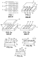
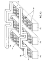
- connections may be made from microscale features 116 not only to straight nanowires 118, but also to systems of curvilinear approximately parallel nanowires; see FIG. 13.
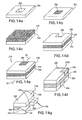
- the superlattice is cut in half through the shadowed regions of material "A". Then the side of the superlattice is exposed to the etch which removes material "B” from between the layers of material "A", as well as from the shadowed regions inside the layers of material "A”. Hence, a unique pattern of protruding regions of material "A” is exposed on the side edge of the superlattice.
- the side of the superlattice can then be used as a mould.
- the width of nanowires is controlled by the thickness of layers "A”. Therefore, the method is capable of producing multiplexers deep into the nano-scale.
- a similar scheme is disclosed and claimed in U.S. Patent 6,294,450, using alternating layers of two dissimilar materials.
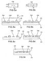
- the opening 52a is next filled with a material 54a having a second composition, as shown in FIG. 14b.
- the process is continued by adding a third layer 50b of the first composition and forming a second opening 52b through that third layer, as shown in FIG. 14d.
- the second opening 52b is formed not over the first opening 52a, but laterally displaced from it.
- the third layer 50b like the previous layers, is of nanoscopic thickness, while the opening 52b, like the opening 52a, has microscopic lateral dimensions.
Landscapes
- Engineering & Computer Science (AREA)
- Chemical & Material Sciences (AREA)
- Nanotechnology (AREA)
- Physics & Mathematics (AREA)
- General Physics & Mathematics (AREA)
- Manufacturing & Machinery (AREA)
- Microelectronics & Electronic Packaging (AREA)
- Condensed Matter Physics & Semiconductors (AREA)
- Crystallography & Structural Chemistry (AREA)
- Mathematical Physics (AREA)
- Computer Hardware Design (AREA)
- Theoretical Computer Science (AREA)
- Power Engineering (AREA)
- Internal Circuitry In Semiconductor Integrated Circuit Devices (AREA)
- Shaping Of Tube Ends By Bending Or Straightening (AREA)
- Exposure Of Semiconductors, Excluding Electron Or Ion Beam Exposure (AREA)
- Moulds For Moulding Plastics Or The Like (AREA)
Applications Claiming Priority (2)
| Application Number | Priority Date | Filing Date | Title |
|---|---|---|---|
| US453329 | 1982-12-27 | ||
| US10/453,329 US7256435B1 (en) | 2003-06-02 | 2003-06-02 | Multilevel imprint lithography |
Publications (2)
| Publication Number | Publication Date |
|---|---|
| EP1484644A2 true EP1484644A2 (de) | 2004-12-08 |
| EP1484644A3 EP1484644A3 (de) | 2006-04-12 |
Family
ID=33159518
Family Applications (1)
| Application Number | Title | Priority Date | Filing Date |
|---|---|---|---|
| EP04252735A Withdrawn EP1484644A3 (de) | 2003-06-02 | 2004-05-12 | Form, Anordnung von Nanoleitungen, Multiplexer/Demultiplexer und dessen Herstellung |
Country Status (3)
| Country | Link |
|---|---|
| US (2) | US7256435B1 (de) |
| EP (1) | EP1484644A3 (de) |
| JP (1) | JP4216766B2 (de) |
Cited By (7)
| Publication number | Priority date | Publication date | Assignee | Title |
|---|---|---|---|---|
| WO2006131838A2 (en) * | 2005-06-06 | 2006-12-14 | Nxp B.V. | Method for manufacturing a crossbar circuit device |
| WO2007089522A1 (en) * | 2006-01-27 | 2007-08-09 | Hewlett-Packard Development Company, L. P. | Mixed-scale electronic interface |
| EP1580596A3 (de) * | 2004-03-23 | 2007-11-28 | Hewlett-Packard Development Company, L.P. | Mit Hilfe einer Nanostrukturen aufweisenden Schablone hergestellte Struktur |
| WO2008138361A1 (en) * | 2007-05-09 | 2008-11-20 | Technische Universität München | Mold for generating nanostructures, and mold holder unit |
| US7931844B2 (en) * | 2005-05-16 | 2011-04-26 | Asml Netherlands B.V. | Imprint lithography |
| US8641912B2 (en) | 2007-05-23 | 2014-02-04 | California Institute Of Technology | Method for fabricating monolithic two-dimensional nanostructures |
| EP2863291A1 (de) * | 2013-10-18 | 2015-04-22 | Applied Materials, Inc. | Transparenter Körper für ein Berührungstafelherstellungsverfahren und System zur Herstellung eines transparenten Körpers für eine Berührungsbildschirmtafel |
Families Citing this family (22)
| Publication number | Priority date | Publication date | Assignee | Title |
|---|---|---|---|---|
| US7602069B2 (en) * | 2004-03-31 | 2009-10-13 | Universität Duisburg-Essen | Micro electronic component with electrically accessible metallic clusters |
| US8025831B2 (en) * | 2004-05-24 | 2011-09-27 | Agency For Science, Technology And Research | Imprinting of supported and free-standing 3-D micro- or nano-structures |
| KR20070010472A (ko) * | 2005-07-19 | 2007-01-24 | 삼성전자주식회사 | 하이브리드형 편광자와, 이의 제조 방법 및 이를 갖는표시장치 |
| WO2007049494A1 (ja) * | 2005-10-25 | 2007-05-03 | National University Corporation Hokkaido University | パターニングされた物質の製造方法 |
| FR2893018B1 (fr) * | 2005-11-09 | 2008-03-14 | Commissariat Energie Atomique | Procede de formation de supports presentant des motifs, tels que des masques de lithographie. |
| JP5213335B2 (ja) * | 2006-02-01 | 2013-06-19 | キヤノン株式会社 | インプリント用モールド、該モールドによる構造体の製造方法 |
| DE102006030267B4 (de) * | 2006-06-30 | 2009-04-16 | Advanced Micro Devices, Inc., Sunnyvale | Nano-Einprägetechnik mit erhöhter Flexibilität in Bezug auf die Justierung und die Formung von Strukturelementen |
| JP5004225B2 (ja) * | 2007-09-19 | 2012-08-22 | 独立行政法人産業技術総合研究所 | インプリントリソグラフィ用モールド製作方法 |
| US20100264560A1 (en) * | 2007-12-19 | 2010-10-21 | Zhuqing Zhang | Imprint lithography apparatus and method |
| US8466068B2 (en) * | 2007-12-31 | 2013-06-18 | Sandisk 3D Llc | Methods and apparatus for forming memory lines and vias in three dimensional memory arrays using dual damascene process and imprint lithography |
| US20100301449A1 (en) * | 2007-12-31 | 2010-12-02 | Sandisk 3D Llc | Methods and apparatus for forming line and pillar structures for three dimensional memory arrays using a double subtractive process and imprint lithography |
| US8114787B2 (en) | 2009-02-19 | 2012-02-14 | Empire Technology Development Llc | Integrated circuit nanowires |
| FR2942738B1 (fr) * | 2009-03-03 | 2016-04-15 | Commissariat A L'energie Atomique | Procede de fabrication d'un moule pour la lithographie par nano-impression |
| FR2942739B1 (fr) * | 2009-03-03 | 2011-05-13 | Commissariat Energie Atomique | Procede de fabrication d'un moule pour la lithographie par nano-impression |
| US8207058B1 (en) * | 2009-06-29 | 2012-06-26 | Georgia Tech Research Corporation | Electron beam induced deposition of interface to carbon nanotube |
| US8450131B2 (en) | 2011-01-11 | 2013-05-28 | Nanohmics, Inc. | Imprinted semiconductor multiplex detection array |
| US8848183B2 (en) | 2011-07-22 | 2014-09-30 | Hewlett-Packard Development Company, L.P. | Apparatus having nano-fingers of different physical characteristics |
| US8883639B2 (en) * | 2012-01-25 | 2014-11-11 | Freescale Semiconductor, Inc. | Semiconductor device having a nanotube layer and method for forming |
| US20140251671A1 (en) * | 2013-03-05 | 2014-09-11 | David Paul Trauernicht | Micro-channel with conductive particle |
| US20140251660A1 (en) * | 2013-03-05 | 2014-09-11 | Ronald Steven Cok | Variable-depth micro-channel structure |
| US9101056B2 (en) * | 2013-03-05 | 2015-08-04 | Eastman Kodak Company | Imprinted bi-layer micro-structure method with bi-level stamp |
| US11338477B2 (en) * | 2016-07-27 | 2022-05-24 | Koninklijke Philips N.V. | Polyorganosiloxane-based stamp manufacturing method, polyorganosiloxane-based stamp, use of the same for a printing process, and an imprinting method using the same |
Family Cites Families (22)
| Publication number | Priority date | Publication date | Assignee | Title |
|---|---|---|---|---|
| US5173442A (en) * | 1990-07-23 | 1992-12-22 | Microelectronics And Computer Technology Corporation | Methods of forming channels and vias in insulating layers |
| US5277749A (en) * | 1991-10-17 | 1994-01-11 | International Business Machines Corporation | Methods and apparatus for relieving stress and resisting stencil delamination when performing lift-off processes that utilize high stress metals and/or multiple evaporation steps |
| US5772905A (en) | 1995-11-15 | 1998-06-30 | Regents Of The University Of Minnesota | Nanoimprint lithography |
| US6256767B1 (en) * | 1999-03-29 | 2001-07-03 | Hewlett-Packard Company | Demultiplexer for a molecular wire crossbar network (MWCN DEMUX) |
| US6599836B1 (en) * | 1999-04-09 | 2003-07-29 | Micron Technology, Inc. | Planarizing solutions, planarizing machines and methods for mechanical or chemical-mechanical planarization of microelectronic-device substrate assemblies |
| EP1065059B1 (de) * | 1999-07-02 | 2007-01-31 | Canon Kabushiki Kaisha | Verfahren zur Herstellung eines Flüssigkeitsausstosskopfes, damit hergestellter Flüssigkeitsausstosskopf, Kopfkassette, Flüssigkeitsausstossvorrichtung, Verfahren zur Herstellung einer Siliziumplatte und damit hergestellte Siliziumplatte |
| US6504292B1 (en) * | 1999-07-15 | 2003-01-07 | Agere Systems Inc. | Field emitting device comprising metallized nanostructures and method for making the same |
| US6294450B1 (en) | 2000-03-01 | 2001-09-25 | Hewlett-Packard Company | Nanoscale patterning for the formation of extensive wires |
| US6350360B1 (en) * | 2000-04-07 | 2002-02-26 | Sandia Coroporation | Method of fabricating a 3-dimensional tool master |
| US6328042B1 (en) * | 2000-10-05 | 2001-12-11 | Lam Research Corporation | Wafer cleaning module and method for cleaning the surface of a substrate |
| US6593238B1 (en) * | 2000-11-27 | 2003-07-15 | Motorola, Inc. | Method for determining an endpoint and semiconductor wafer |
| US6882051B2 (en) * | 2001-03-30 | 2005-04-19 | The Regents Of The University Of California | Nanowires, nanostructures and devices fabricated therefrom |
| US6893705B2 (en) * | 2001-05-25 | 2005-05-17 | Massachusetts Institute Of Technology | Large area orientation of block copolymer microdomains in thin films |
| US6432740B1 (en) * | 2001-06-28 | 2002-08-13 | Hewlett-Packard Company | Fabrication of molecular electronic circuit by imprinting |
| WO2003030252A2 (en) * | 2001-09-28 | 2003-04-10 | Hrl Laboratories, Llc | Process for producing interconnects |
| US6936181B2 (en) * | 2001-10-11 | 2005-08-30 | Kovio, Inc. | Methods for patterning using liquid embossing |
| US6743368B2 (en) * | 2002-01-31 | 2004-06-01 | Hewlett-Packard Development Company, L.P. | Nano-size imprinting stamp using spacer technique |
| US6861365B2 (en) * | 2002-06-28 | 2005-03-01 | Hewlett-Packard Development Company, L.P. | Method and system for forming a semiconductor device |
| JP3821069B2 (ja) | 2002-08-01 | 2006-09-13 | 株式会社日立製作所 | 転写パターンによる構造体の形成方法 |
| US20040112862A1 (en) * | 2002-12-12 | 2004-06-17 | Molecular Imprints, Inc. | Planarization composition and method of patterning a substrate using the same |
| EP1606834B1 (de) * | 2003-03-27 | 2013-06-05 | Korea Institute Of Machinery & Materials | Uv-nanoimprint-lithografieverfahren unter verwendung eines elementweisen prägestempels |
| US6897098B2 (en) * | 2003-07-28 | 2005-05-24 | Intel Corporation | Method of fabricating an ultra-narrow channel semiconductor device |
-
2003
- 2003-06-02 US US10/453,329 patent/US7256435B1/en not_active Expired - Lifetime
-
2004
- 2004-05-12 EP EP04252735A patent/EP1484644A3/de not_active Withdrawn
- 2004-05-24 JP JP2004153541A patent/JP4216766B2/ja not_active Expired - Fee Related
-
2006
- 2006-12-07 US US11/636,264 patent/US7803712B2/en not_active Expired - Fee Related
Non-Patent Citations (1)
| Title |
|---|
| TANIGUCHI ET AL., 3D IMPRINT TECHNOLOGY USING SOG MOLD |
Cited By (16)
| Publication number | Priority date | Publication date | Assignee | Title |
|---|---|---|---|---|
| EP1580596A3 (de) * | 2004-03-23 | 2007-11-28 | Hewlett-Packard Development Company, L.P. | Mit Hilfe einer Nanostrukturen aufweisenden Schablone hergestellte Struktur |
| US7597814B2 (en) | 2004-03-23 | 2009-10-06 | Hewlett Packard Development Company, L.P. | Structure formed with template having nanoscale features |
| US7833842B2 (en) | 2004-11-03 | 2010-11-16 | Hewlett-Packard Development Company, L.P. | Mixed-scale electronic interface |
| US7931844B2 (en) * | 2005-05-16 | 2011-04-26 | Asml Netherlands B.V. | Imprint lithography |
| WO2006131838A3 (en) * | 2005-06-06 | 2007-02-22 | Koninkl Philips Electronics Nv | Method for manufacturing a crossbar circuit device |
| WO2006131838A2 (en) * | 2005-06-06 | 2006-12-14 | Nxp B.V. | Method for manufacturing a crossbar circuit device |
| CN101375344B (zh) * | 2006-01-27 | 2012-04-04 | 惠普开发有限公司 | 混合尺度电子接口 |
| WO2007089522A1 (en) * | 2006-01-27 | 2007-08-09 | Hewlett-Packard Development Company, L. P. | Mixed-scale electronic interface |
| US7544977B2 (en) | 2006-01-27 | 2009-06-09 | Hewlett-Packard Development Company, L.P. | Mixed-scale electronic interface |
| EP2096672A2 (de) | 2006-01-27 | 2009-09-02 | Hewlett-Packard Development Company, L.P. | Elektronische Schnittstelle im Mischmaßstab und Herstellungsverfahren |
| EP2096672A3 (de) * | 2006-01-27 | 2010-01-13 | Hewlett-Packard Development Company, L.P. | Elektronische Schnittstelle im Mischmaßstab und Herstellungsverfahren |
| WO2008138361A1 (en) * | 2007-05-09 | 2008-11-20 | Technische Universität München | Mold for generating nanostructures, and mold holder unit |
| US8641912B2 (en) | 2007-05-23 | 2014-02-04 | California Institute Of Technology | Method for fabricating monolithic two-dimensional nanostructures |
| EP2863291A1 (de) * | 2013-10-18 | 2015-04-22 | Applied Materials, Inc. | Transparenter Körper für ein Berührungstafelherstellungsverfahren und System zur Herstellung eines transparenten Körpers für eine Berührungsbildschirmtafel |
| WO2015055830A1 (en) * | 2013-10-18 | 2015-04-23 | Applied Materials, Inc. | Transparent body for a touch panel manufacturing method and system for manufacturing a transparent body for a touch screen panel |
| US9920421B2 (en) | 2013-10-18 | 2018-03-20 | Applied Materials, Inc. | Transparent body for a touch panel manufacturing method and system for manufacturing a transparent body for a touch screen panel |
Also Published As
| Publication number | Publication date |
|---|---|
| EP1484644A3 (de) | 2006-04-12 |
| JP4216766B2 (ja) | 2009-01-28 |
| JP2004363584A (ja) | 2004-12-24 |
| US7256435B1 (en) | 2007-08-14 |
| US7803712B2 (en) | 2010-09-28 |
| US20100112809A1 (en) | 2010-05-06 |
Similar Documents
| Publication | Publication Date | Title |
|---|---|---|
| US7803712B2 (en) | Multilevel imprint lithography | |
| JP4674366B2 (ja) | ナノスケールフィーチャを備えたテンプレートが形成されている構造体およびその作製方法 | |
| US8486511B2 (en) | Pattern formation employing self-assembled material | |
| Ross et al. | Three‐dimensional nanofabrication by block copolymer self‐assembly | |
| KR102225696B1 (ko) | 연결 배선 구조체 형성 방법 | |
| US8562795B2 (en) | Nanoscale electric lithography | |
| US20070228523A1 (en) | Reduction of a feature dimension in a nano-scale device | |
| WO2003049151A2 (en) | Fabrication of molecular electronic circuit by imprinting | |
| KR102166523B1 (ko) | 나노 스케일 형상 구조 및 형성 방법 | |
| JP2012527773A (ja) | 離間された導電配線に電気的接続を提供する方法 | |
| CN1961259B (zh) | 超晶格的制造和使用 | |
| US7662659B2 (en) | Methods of forming arrays of nanoscale building blocks | |
| US20100052177A1 (en) | Method for manufacturing a crossbar circuit device | |
| Crawley et al. | 3D molecular interconnection technology | |
| Cui et al. | Indirect Nanofabrication | |
| TWI382454B (zh) | 自我校準交叉點記憶體製造技術 | |
| JP2007027595A (ja) | 集積回路装置の製造方法 | |
| KR20180026157A (ko) | 듀얼 다마신 공정을 이용한 배선 구조체 형성 방법 | |
| JP2010228448A (ja) | ナノインプリンティングによってリソグラフィのためのモールドを製造する方法 |
Legal Events
| Date | Code | Title | Description |
|---|---|---|---|
| PUAI | Public reference made under article 153(3) epc to a published international application that has entered the european phase |
Free format text: ORIGINAL CODE: 0009012 |
|
| AK | Designated contracting states |
Kind code of ref document: A2 Designated state(s): AT BE BG CH CY CZ DE DK EE ES FI FR GB GR HU IE IT LI LU MC NL PL PT RO SE SI SK TR |
|
| AX | Request for extension of the european patent |
Extension state: AL HR LT LV MK |
|
| PUAL | Search report despatched |
Free format text: ORIGINAL CODE: 0009013 |
|
| AK | Designated contracting states |
Kind code of ref document: A3 Designated state(s): AT BE BG CH CY CZ DE DK EE ES FI FR GB GR HU IE IT LI LU MC NL PL PT RO SE SI SK TR |
|
| AX | Request for extension of the european patent |
Extension state: AL HR LT LV MK |
|
| 17P | Request for examination filed |
Effective date: 20060925 |
|
| AKX | Designation fees paid |
Designated state(s): DE FR GB |
|
| 17Q | First examination report despatched |
Effective date: 20100617 |
|
| STAA | Information on the status of an ep patent application or granted ep patent |
Free format text: STATUS: THE APPLICATION IS DEEMED TO BE WITHDRAWN |
|
| 18D | Application deemed to be withdrawn |
Effective date: 20131201 |