Technical Field
The present invention relates to a supporting
mechanism used for transferring a target substrate,
such as a semiconductor wafer, in cooperation with
a transfer arm, in a semiconductor processing system.
The term "semiconductor process" used herein includes
various kinds of processes which are performed to
manufacture a semiconductor device or a structure
having wiring layers, electrodes, and the like to be
connected to a semiconductor device, on a target
substrate, such as a semiconductor wafer or an LCD
substrate, by forming semiconductor layers, insulating
layers, and conductive layers in predetermined patterns
on the target substrate.
Background Art
In the process of manufacturing semiconductor
integrated circuits, a wafer is subjected to various
processes, such as film-formation, etching, oxidation,
and diffusion. Owing to the demands of increased
miniaturization and integration of semiconductor
integrated circuits, the throughput and yield involving
these processes need to be increased. In light of
this, there is a semiconductor processing system of the
so-called cluster tool type, which has a plurality of
process chambers for performing the same process, or a
plurality of process chambers for performing different
processes, connected to a common transfer chamber.
With a system of this type, various steps can be
performed in series, without exposing a wafer to air.
For example, Jpn. Pat. Appln. KOKAI Publication
Nos. 2000-208589 and 2000-299367 disclose a semiconductor
processing system of the cluster tool type.
In a semiconductor processing system of the
cluster tool type, there are a plurality of transfer
arms for transferring a semiconductor wafer. Each
transfer arm is arranged to extend, contract, and
rotate or move horizontally. The transfer arms
sequentially transfer a wafer among them from a wafer
cassette to processing apparatuses or vice versa.
In general, transfer of a wafer between transfer
arms is not directly performed therebetween, but via a
supporting mechanism disposed therebetween, which can
move the wafer up and down, or a buffer table having
such a supporting mechanism. The wafer is transferred
onto the supporting mechanism or buffer table by one of
the transfer arms, and is then transferred from the
supporting mechanism or buffer table by the other of
the transfer arms.
Depending on the processing manner of a wafer,
the wafer is temporarily kept waiting in a transfer
chamber in the middle of transfer, and another wafer is
transferred by priority. In this case, the transfer
chamber may be provided with a supporting mechanism or
buffer table as that described above. For example,
Jpn. Pat. Appln. KOKAI Publication Nos. 4-69917,
9-223727, and 2001-176947 disclose a supporting
mechanism or buffer table of this kind.
In handling semiconductor wafers for a film-formation
process, for example, there is a case where
processed wafers are accompanied by thin films sticking
to the bottom, as well as the top as a matter of
course. In this case, if lifter pins or the like come
into direct contact with the bottom of wafers to handle
them, unprocessed wafers are contaminated with film
particles transferred from the lifter pins.
Furthermore, the supporting mechanisms disclosed
in the publications mentioned above include two lifters
for moving a wafer up and down, which are used at the
same time to transfer a wafer. Accordingly, it is
difficult to use the supporting mechanisms flexibly in
light of the situation.
Disclosure of Invention
An object of the present invention is to provide
a substrate supporting mechanism for a semiconductor
processing system, which includes two holding portions
alternatively usable in light of the situation, and has
a compact structure.
According to an aspect of the present invention,
there is provided a supporting mechanism used for
transferring a target substrate in cooperation with
a transfer arm, in a semiconductor processing system,
the supporting mechanism comprising:
Brief Description of Drawings
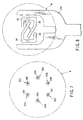
FIG. 1 is a schematic plan view showing a
semiconductor processing system including a substrate
supporting mechanism according to a first embodiment of
the present invention;
FIG. 2 is a sectional view showing an intermediate
chamber having a load-lock function and provided with
the supporting mechanism shown in FIG. 1;
FIG. 3 is a perspective view of the supporting
mechanism shown in FIG. 1;
FIG. 4 is a plan view of the supporting mechanism
shown in FIG. 1;
FIG. 5 is an enlarged partial view showing the
supporting structure of a reciprocation rod used in the
supporting mechanism shown in FIG. 1;
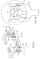
FIG. 6 is a view schematically showing the
placement of actuators used in a supporting mechanism
according to a second embodiment of the present
invention;
FIG. 7 is a plan view showing the placement of
lifter pins used in the supporting mechanism shown in
FIG. 6;
FIG. 8 is a plan view showing base frames used in
a supporting mechanism according to a third embodiment
of the present invention;
FIG. 9 is a perspective view showing a supporting
mechanism according to a fourth embodiment of the
present invention;
FIG. 10 is a plan view showing the supporting
mechanism shown in FIG. 9;
FIG. 11 is a perspective view showing a supporting
mechanism according to a fifth embodiment of the
present invention;
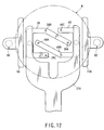
FIG. 12 is a plan view showing the supporting
mechanism shown in FIG. 11;
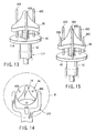
FIG. 13 is a perspective view showing a supporting
mechanism according to a sixth embodiment of the
present invention;
FIG. 14 is a plan view showing the supporting
mechanism shown in FIG. 13; and
FIG. 15 is a view showing a supporting mechanism
according to a modification of the sixth embodiment.
Best Mode for Carrying Out the Invention
Embodiments of the present invention will be
described hereinafter with reference to the accompanying
drawings. In the following description, the
constituent elements having substantially the same
function and arrangement are denoted by the same
reference numerals, and a repetitive description will
be made only when necessary.
<First embodiment>
FIG. 1 is a schematic plan view showing a
semiconductor processing system including a substrate
supporting mechanism according to a first embodiment of
the present invention.
As shown in FIG. 1, the processing system 2
includes a plurality of, e.g., four processing
apparatuses 4A, 4B, 4C, and 4D, an almost hexagonal
common transfer chamber 6, first and second
intermediate chambers (load-lock chambers) 8A and 8B,
and a thin and long entrance transfer chamber 10.
The intermediate chambers 8A and 8B are respectively
provided with substrate supporting mechanisms 12A and
12B. Each of the common transfer chamber 6 and first
and second intermediate chambers 8A and 8B are formed
of an airtight chamber, which can be vacuum exhausted.
More specifically, the processing apparatuses 4A
to 4D are respectively connected to four sides of the
almost hexagonal common transfer chamber 6, and the
first and second intermediate chambers 8A and 8B are
respectively connected to the other two sides thereof.
In other words, the processing system 2 has a structure
of the cluster tool type in which the processing
apparatuses and intermediate chambers are connected to
and around the common transfer chamber 6. The entrance
transfer chamber 10 is connected to the first and
second intermediate chambers 8A and 8B in common.
The processing apparatuses 4A to 4D and first and
second intermediate chambers 8A and 8B are connected to
the common transfer chamber 6 respectively through gate
valves G1 to G4, and G5 and G6, which are airtightly
opened and closed. The first and second intermediate
chambers 8A and 8B are connected to the entrance
transfer chamber 10 respectively through gate valves G7
and G8, which are airtightly opened and closed.
The four processing apparatuses 4A to 4D are
designed to perform the same process or different
processes on a target substrate or semiconductor wafer
in a vacuum atmosphere. The common transfer chamber 6
is provided with first transfer means 14 disposed
therein at a position to access the two intermediate
chambers 8A and 8B and four processing apparatuses 4A
to 4D. The first transfer means 14 is formed of an
articulated arm that can extend, contract, and rotate.
The first transfer means 14 has two picks 14A and 14B,
which can independently extend and contract in opposite
directions, so that it can handle two wafers at a time.
Alternatively, the first transfer means 14 may have
only one pick.
The entrance transfer chamber 10 has a long thin
box-type configuration in which an inactive gas, such
as N2 gas, or clean air is circulated. One or more
cassette tables, e.g., three cassette tables 16A, 16B,
and 16C in this example, are disposed on one side of
this laterally long box. The cassette tables 16A, 16B,
and 16C are configured to place cassettes 18A to 18C
thereon, respectively.
Each of the cassettes 18A to 18C is structured to
store, e.g., 25 wafers W at most, at regular intervals
in the vertical direction. Each of the cassettes 18A
to 18C has an airtight structure filled with, e.g.,
an N2 gas atmosphere. Wafers are transferred into and
from the entrance transfer chamber 10 through gate
doors 20A, 20B, and 20C disposed correspondingly to
the cassette tables 16A to 16C.
The entrance transfer chamber 10 is provided
with second transfer means 22 disposed therein, for
transferring wafers W in its longitudinal direction.
The second transfer means 22 is supported on and slides
along a guide rail 24 that extends in the longitudinal
direction at the center of the entrance transfer
chamber 10. The guide rail 24 has an actuating
mechanism, such as a linear motor, built therein.
The linear motor moves the second transfer means 22 on
the guide rail 24 in an X-direction.
An alignment device or orientor 26 for performing
alignment of a wafer is disposed at one end of the
entrance transfer chamber 10. The orientor 26 includes
a rotary table 28, which is rotated by a driving
motor (not shown), along with a wafer W placed thereon.
An optical sensor 30 is disposed beside the rotary
table 28, for detecting the periphery of the wafer W.
The optical sensor 30 is used to detect the direction
and misalignment of the notch or orientation flat of
the wafer W.
The second transfer means 22 has two transfer arms
32 and 34 formed of articulated arms and disposed on
upper and lower sides. The transfer arms 32 and 34
respectively have fork- like picks 32A and 34A at their
distal ends, on each of which a wafer W is directly
held. Each of the transfer arms 32 and 34 can extend
and contract in a radial direction R from the center.
The transfer arms 32 and 34 can be controlled to extend
and contract independently of each other. The transfer
arms 32 and 34 can integratedly rotate in the angular
direction relative to a base 36.
Next, an explanation will be given of the
supporting mechanisms 12A and 12B respectively disposed
in the intermediate chambers 8A and 8B. Since the two
supporting mechanisms 12A and 12B have completely the
same structure, only one of them, e.g., the supporting
mechanism 12A will be exemplified.
FIG. 2 is a sectional view showing an intermediate
chamber having a load-lock function and provided with
the supporting mechanism shown in FIG. 1. FIGS. 3 and
4 are a perspective view and a plan view, respectively,
of the supporting mechanism shown in FIG. 1
As shown in FIGS. 2 to 4, the supporting mechanism
12A includes a plurality of, e.g., two in this example,
base frames 38 and 40, each of which is formed of
a thin plate bar bent to form a numeral "7" shape,
and made of, e.g., aluminum or ceramic. The two base
frames 38 and 40 are disposed not to overlap with each
other in the plan view, so that they do not hit or
interfere with each other when they are moved up and
down. As shown in FIGS. 3 and 4, the base frames 38
and 40 have extension portions 39 and 41, which extend
toward each other and mutually beyond their tips into
cut spaces in the base frames.
Each of the base frames 38 and 40 is provided
with a plurality of, e.g., three in this embodiment,
lifter pins 38A to 38C or 40A to 40C standing upward
therefrom. The lifter pins 38A to 38C and 40A to 40C
are made of ceramic, such as Al2O3. Each group of
lifter pins 38A to 38C and 40A to 40C supports a wafer
W, while their top ends are in direct contact with the
bottoms of the wafers.
As shown also in FIG. 4, each group of lifter pins
38A to 38C and 40A to 40C are disposed along one common
circle 42 at regular intervals (intervals of about 120
degrees). The number of lifter pins disposed on one
base frame 38 or 40 needs to be at least three. The
two groups of the lifter pins 38A to 38C and 40A to 40C
may be respectively disposed along different circles.
The two actuators 46 and 48 are disposed at the
bottom plate 44 (see FIG. 2) of the intermediate
chamber 8A, and used for the two base frames 38 and 40,
respectively. The actuators 46 and 48 include
reciprocation rods 50 and 52, which extend through
holes 54 and 56 formed in the bottom plate 44, and
connected or fixed at the top to the bottoms of the
base frames 38 and 40, respectively. The actuators 46
and 48 can move up and down the base frames 38 and 40
independently of each other.
The actuators 46 and 48 are set to give the same
stroke of the vertical movement to the lifter pins 38A
to 38C and lifter pins 40A to 40C. Furthermore, the
uppermost and lowermost positions of the top ends of
the lifter pins 38A to 38C are essentially the same as
the uppermost and lowermost positions of the top ends
of the lifter pins 40A to 40C. In other words, the
lifter pins 38A to 38C and lifter pins 40A to 40C share
essentially the same position where a wafer W is
transferred to and from the first transfer means 14 or
second transfer means 22. However, even if the two
members have different vertical strokes or different
uppermost and lowermost positions, a wafer W can be
transferred to and from the first and second transfer
means 14 and 22, using vertical movement of the first
and second transfer means 14 and 22.
Those portions of the bottom plate 44, where
the reciprocation rods 50 and 52 penetrate, are
respectively provided with bellows 58 and 60 each
formed of, e.g., a longitudinally flexible metal
accordion hose. More specifically, as shown in FIG. 5,
the reciprocation rods 50 and 52 are respectively
inserted in the bellows 58 and 60. The upper ends of
the bellows 58 and 60 are airtightly connected to the
bottoms of the base frames 38 and 40, respectively.
The lower ends of the bellows 58 and 60 are airtightly
fixed to the bottom of the bottom plate 44 by screws
66 each through a seal member 62 and an attachment
ring 64.
The bellows 58 and 60 thus arranged maintain
the interior of the intermediate chamber 8A airtight,
while allowing the reciprocation rods 50 and 52 to be
moved up and down. A vertical movement controller 68
formed of, e.g., a microcomputer is used to control the
operation of the actuators 46 and 48.
Each of the intermediate chambers 8A and 8B has
a port 70 for feeding an inactive gas, such as N2 gas,
and an exhaust port 72 connected to a vacuum exhaust
section (not shown), wherein the ports are formed in,
e.g., the bottom of the chamber. This arrangement is
used to set the pressure inside the intermediate
chambers 8A and 8B between a vacuum atmosphere and
atmospheric pressure atmosphere, as needed.
Next, an explanation will be given of an outline
of the flow of a wafer W, in relation to the
semiconductor processing system shown in FIG. 1.
First, an unprocessed wafer W is picked up from
one of the cassettes placed on the three cassette
tables 16A to 16C, e.g., the cassette 18C placed on the
cassette table 16C. At this time, one of the transfer
arms of the second transfer means 22, e.g., the
transfer arm 32, is operated to pick up and hold
the wafer W from the cassette 18C by the pick 32A.
Then, the second transfer means 22 is moved in the
X-direction to transfer the wafer W to the orientor 26.
Then, an unprocessed wafer W, which has been
aligned by the orientor 26, is taken out of the rotary
table 28 to make the rotary table 28 free. For this
purpose, the other transfer arm 34, which is
unoccupied, is operated to pick up and hold, by the
pick 34A, the wafer W from the rotary table 28.
Then, the transfer arm 32 is operated to place
the unprocessed wafer held on the pick 32A onto the
unoccupied rotary table 28. This wafer is subjected
to alignment by the time when a next unprocessed wafer
is transferred thereto. Then, the second transfer
means 22 is moved in the X-direction to transfer the
unprocessed wafer, which has been taken out of the
rotary table 28 by the other transfer arm 34, to one
of the two intermediate chambers 8A and 8B, e.g., the
intermediate chamber 8A.
Then, the gate valve G7 is opened to open the
intermediate chamber 8A, which has been adjusted in
pressure. At this time, a processed wafer that has
been subjected to a predetermined process, such as a
film-formation process or etching process, is waiting
on one of the groups of the lifter pins, e.g., lifter
pins 40A to 40C in the intermediate chamber 8A.
Then, the unoccupied transfer arm 32 is operated
to pick up and hold, by the pick 32A, the processed
wafer W waiting on the lifter pins 40A to 40C. Then,
the other transfer arm 34 is operated to place the
unprocessed wafer held on the pick 34A onto the other
group of lifter pins 38A to 38C. On the other hand,
the processed wafer is returned back to the original
cassette by the second transfer means 22.
After the unprocessed wafer W is placed on the
lifter pins 38A to 38C, the gate valve G7 is closed to
make the intermediate chamber 8A airtight. Then, the
pressure in the intermediate chamber 8A is adjusted by
vacuum exhaust. Then, the gate valve G5 is opened to
cause the intermediate chamber 8A to communicate with
the common transfer chamber 6, which has been set to
have a vacuum atmosphere in advance. Then, the first
transfer means 14 in the common transfer chamber 6 is
operated to pick up the unprocessed wafer W. At this
time, if a processed wafer is held on the first
transfer means 14, the processed wafer is replaced with
the unprocessed wafer, using the two picks 14A and 14B
of the first transfer means 14.
Then, the unprocessed wafer W is sequentially
subjected to the necessary processes in the processing
apparatuses 4A to 4D, for example. After the necessary
processes are completed, the processed wafer W is
returned back to the original cassette, through a route
reverse to that described above. At this time, the
processed wafer W can be transferred through either one
of the two intermediate chambers 8A and 8B. When the
processed wafer W is held in the intermediate chambers
8A and 8B, the lifter pins 40A to 40C are used, which
belong to a group other than the group used for holding
the unprocessed wafer W. As a consequence, the
unprocessed wafer W is prevented, as far as possible,
from being contaminated by contaminants, such as thin
films.
Next, a detailed explanation will be given as to
how a wafer W is transferred in the intermediate
chamber 8A. Wafer transfer in the other intermediate
chamber 8B is performed in the same manner.
In this embodiment, as described above,
unprocessed wafers W are handled by a group of lifter
pins different from a group used for handling processed
wafers W, to prevent contamination of the wafers W.
For example, the three lifter pins 38A to 38C disposed
on the base frame 38 are exclusively used for
supporting unprocessed wafers W, while the three lifter
pins 40A to 40C disposed on the other base frame 40 are
exclusively used for supporting processed wafers W.
The following explanation will take as an example a
case where an unprocessed wafer W transferred in from
the entrance transfer chamber 10, and a processed wafer
W is replaced with the unprocessed wafer W.
First, the lifter pins 40A to 40C of the base
frame 40 supporting the processed wafer W are placed at
an upper position, and the unoccupied lifter pins 38A
to 38C of the other base frame 38 are placed at a lower
position. In this sate, the unoccupied pick 32A is
moved in a horizontal direction into the intermediate
chamber 8A, and inserted into a position below the
processed wafer W (between the wafer W and base frame
40). Then, the lifter pins 40A to 40C are moved down
to transfer the processed wafer W onto the pick 32A.
Then, the pick 32A is moved backward to retreat from
the intermediate chamber 8A.
Then, the other pick 34A holding the unprocessed
wafer W is moved in a horizontal direction into the
intermediate chamber 8A. Then, the other base frame 38
at the lower position is moved up, so that the lifter
pins 38A to 38C receive the unprocessed wafer W from
below. Then, the unoccupied pick 34A is moved backward
to retreat from the intermediate chamber 8A. As a
consequence, the processed wafer W is replaced with the
unprocessed wafer W. Basically the same operation is
performed when a wafer W is transferred between the
common transfer chamber 6 and intermediate chamber 8A.
In the operation described above, the lifter
pins 38A to 38C keep supporting the unprocessed wafer
W until the wafer W is transferred onto the first
transfer means 14, after receiving the wafer W from the
second transfer means 22. During this time, the lifter
pins 40A to 40C support no wafer W. On the other
hand, the lifter pins 40A to 40C keep supporting the
processed wafer W until the wafer W is transferred
onto the second transfer means 22, after receiving the
wafer W from the first transfer means 14. During this
time, the lifter pins 38A to 38C support no wafer W.
In summary, the lifter pins 38A to 38C and the lifter
pins 40A to 40C alternatively support a wafer W. This
matter is also common to the following embodiments.
The two groups of the lifter pins 38A to 38C and lifter
pins 40A to 40C can be arbitrarily set to be used
either for unprocessed wafers W or for processed
wafers W.
The first embodiment includes a plurality of,
e.g., two, base frames 38 and 40, each having a
plurality of, e.g., three, lifter pins 38A to 38C
or 40A to 40C disposed thereon. One group of lifter
pins 38A to 38C is exclusively used for transferring
unprocessed wafers W, and the other group of lifter
pins 40A to 40C is exclusively used for transferring
processed wafers W. As a consequence, unprocessed
wafers W are prevented from being contaminated by
substances or particles derived from thin films.
Furthermore, even if one of the base frames or
actuators malfunctions, the other base frame can keep
operating to move up and down to transfer a wafer W,
as described above. Accordingly, this improves the
flexibility of usage.
The first embodiment includes the two base frames
38 and 40, but may have a third base frame or more,
which are disposed not to interfere with the two base
frames 38 and 40, and each provided with lifter pins,
as described above.
The supporting mechanisms disclosed in the
publication mentioned in "Background Art" include
two lifters for moving a wafer up and down, and
transfer a wafer, using the two lifters at the same
time. Accordingly, it is difficult to use the
supporting mechanisms flexibly in light of the
situation. More specifically, for example, the
supporting mechanism disclosed in Jpn. Pat. Appln.
KOKAI Publication No. 9-223727 includes two sets of
target substrate supporting means (support pins), which
can be moved independently of each other. The two sets
of supporting means support only one target substrate
in cooperation with each other, or the two sets of
supporting means simultaneously and respectively
support an unprocessed target substrate and a processed
target substrate.
On the other hand, the substrate supporting
mechanism according to the first embodiment includes
two (a plurality of) sets of target substrate
supporting means (corresponding to the two base frames
38 and 40 in this embodiment), which are disposed not
to interfere with each other, and support target
substrates W at substantially the same horizontal
coordinate position to transfer them to and from
a transfer unit. The two (a plurality of) sets of
target substrate supporting means alternatively support
a target substrate (only one set of supporting means
supports one target substrate at a time). In other
words, when one set of supporting means supports
a target substrate, the other set of supporting means
supports no target substrate. Accordingly, the
supporting mechanism according to the first embodiment
has a structure completely different from that of the
prior art described above. This matter is also common
to the following embodiments.
<Second embodiment>
The first embodiment includes a plurality of,
e.g., two, base frames each provided with a plurality
of, e.g., three, lifter pins 38A to 38C or 40A to 40C.
Instead, there may be lifter pins 38A to 38C and 40A to
40C respectively provided with actuators one by one.
In such an aspect, FIG. 6 is a view schematically
showing the placement of actuators used in a supporting
mechanism according to a second embodiment of the
present invention. FIG. 7 is a plan view showing
the placement of lifter pins used in the supporting
mechanism shown in FIG. 6.
As shown in FIG. 6, the lifter pins 38A to 38C
and 40A to 40C are divided into two groups, i.e.,
a first group of lifter pins 38A to 38C and a second
group of lifter pins 40A to 40C. The lifter pins are
respectively provided with actuators 80A to 80C and 82A
to 82C correspondingly disposed therebelow.
As shown in FIG. 7, the actuators 80A to 80C and
82A to 82C are disposed along one circle, but FIG. 6
shows them on one plane, for the sake of comprehension.
It may be arranged such that one group of actuators 80A
to 80C are disposed on one circle, and the other group
of actuators 82A to 82C are disposed along a different
circle. The lifter pins 38A to 38C and 40A to 40C are
respectively connected to the tips of the reciprocation
rods 84A to 84C and 86A to 86C of the actuators 80A to
80C and 82A to 82C. The vertical movement of the
actuators 80A to 80C and 82A to 82C are controlled by
a vertical movement controller 68. Those portions of
the intermediate chamber bottom plate 44, where the
reciprocation rods 84A to 84C and 86A to 86C penetrate,
are respectively provided with bellows 88.
The actuators 80A to 80C connected to one group
of lifter pins 38A to 38C are operated to perform
synchronous vertical movement. Similarly, the
actuators 82A to 82C connected to the other group of
lifter pins 40A to 40C are operated to perform
synchronous vertical movement. The group of actuators
80A to 80C and the group of actuators 82A to 82C can
be controlled independently of each other to perform
vertical movement.
Also in the second embodiment, each group of
lifter pins, i.e., the group of lifter pins 38A to
38C or lifter pins 40A to 40C, are controlled to
synchronously move up and down. As a consequence,
the second embodiment can provide the same operation
and effect as those of the first embodiment described
above. For example, one group of lifter pins 38A to
38C is exclusively used for transferring unprocessed
wafers W, and the other group of lifter pins 40A to
40C is exclusively used for transferring processed
wafers W.
<Third embodiment>
The first embodiment includes a plurality of,
e.g., two, base frames each provided with a plurality
of, e.g., three, lifter pins 38A to 38C or 40A to 40C.
Instead, there may be base frames 38 and 40 provided
with no lifter pins 38A to 38C and 40A to 40C, but
configured to function as holder plates, each of which
comes into direct contact with the bottom of a wafer W
to support it by the top face. In such an aspect,
FIG. 8 is a plan view showing base frames (holder
plates) used in a supporting mechanism according to
a third embodiment of the present invention.
As shown in FIG. 8, the two base frames 38 and 40
are provided with no lifter pins thereon. Each of the
base frames 38 and 40 come into direct contact with the
bottom of a wafer W to support the wafer W. It should
be noted that the two base frames 38 and 40 are
arranged not to interfere with a pick, e.g., pick 32A,
during transfer of a wafer. For this reason, the base
frames 38 and 40 shown in FIG. 8 has a smaller size
than the base frames 38 and 40 of the first embodiment
shown in FIG. 3. The third embodiment can also provide
the same operation and effect as those of the first
embodiment described above.
<Fourth embodiment>
The second embodiment includes no base frames, but
includes lifter pins directly connected to reciprocation
rods. The third embodiment includes no lifter
pins, but includes base frames configured to directly
support a wafer. These features of them can be
combined for use. In such an aspect, FIG. 9 is
a perspective view showing a supporting mechanism
according to a fourth embodiment of the present
invention. FIG. 10 is a plan view showing the
supporting mechanism shown in FIG. 9.
As shown in FIGS. 9 and 10, this supporting
mechanism includes lifter pins 38A and 40A provided
with an associated structure the same as that shown in
FIGS. 6 and 7. Specifically, the two lifter pins 38A
and 40A are directly connected to the reciprocation rod
84A of an actuator 80A and the reciprocation rod 86A of
an actuator 82A, respectively. However, the supporting
mechanism includes no other lifter pins 38B, 38C, 40B,
and 40C (see FIG. 3), but includes base frames 38 and
40 the same as those of the third embodiment shown in
FIG. 8 to compensate for the function of the omitted
lifter pins. Specifically, each of the base frames 38
and 40 is arranged to directly support the bottom of
a wafer. In this case, however, the base frames 38
and 40 do not have a numeral "7" shape shown in FIG. 4,
but have, e.g., a "U" shape, formed by excluding the
portion that supports the lifter pin 38A or 40A.
In this case, the lifter pin 38A and base frame 38
form one group and are synchronously moved up and down.
Also, the other lifter pins 40A and base frame 40 form
one group and are synchronously moved up and down.
The fourth embodiment can also provide the same
operation and effect as those of the first embodiment
described above.
<Fifth embodiment>
Each of the first to fourth embodiments cannot
handle two wafers at a time, but handles always only
one wafer. However, means for secondarily supporting
a wafer may be disposed to handle a plurality of, e.g.,
two, wafers at a time. In such an aspect, FIG. 11 is
a perspective view showing a supporting mechanism
according to a fifth embodiment of the present
invention. FIG. 12 is a plan view showing the
supporting mechanism shown in FIG. 11.
As shown in FIGS. 11 and 12, a supporting
mechanism according to any one of the first to fourth
embodiments is disposed at the center of an
intermediate chamber 8A. A pair of reciprocation rods
90 and 92 are disposed outside the vertical movement
area where a wafer W is moved up and down by the
supporting mechanism. The reciprocation rods 90 and 92
are disposed at positions shifted by 90 degrees from
gate valves G5 and G7 provided on opposite sides of the
intermediate chamber 8A, so that they do not interfere
with a pick 14A, 14B, 32A, or 34A to be inserted when
a wafer is transferred into and out of the intermediate
chamber 8A. FIGS. 11 and 12 shows a case where the
supporting mechanism according to the first embodiment
is disposed at the center of the intermediate chamber
8A. Those portions of the bottom plate 44 of the
intermediate chamber, where the reciprocation rods 90
and 92 penetrate, are respectively provided with
bellows 94 and 96, which maintain the interior of the
intermediate chamber airtight, while allowing the
reciprocation rods 90 and 92 to be moved up and down.
The reciprocation rods 90 and 92 are respectively
moved up and down by actuators (not shown) disposed
therebelow, which perform synchronous vertical
movement. The reciprocation rods 90 and 92 are moved
up and down by a stroke larger than that of the
reciprocation rods 50 and 52. The reciprocation rods
90 and 92 may be connected to each other at the bottom,
so that only one actuator suffices for them.
Support plates 98 and 100 made of, e.g., ceramic
are respectively fixed to the tops of the reciprocation
rods 90 and 92, and horizontally extend toward the
center of the intermediate chamber 8A. The support
plates 98 and 100 have a "T" shape in this embodiment,
with top faces to hold a wafer W transferred by the
first and second transfer means 14 and 22, while they
are in direct contact with the bottom of the wafer W.
The other intermediate chamber 8B is also provided with
the same supporting mechanism as that disposed in the
intermediate chamber 8A, as described above.
According to the fifth embodiment having the
arrangement described above, the lifter pins 38A to
38C and 40A to 40C are operated, as in the first
embodiment, while the pair of support plates 98 and 100
hold an unprocessed wafer W at a higher position, as
shown in FIG. 11, for example. In other words, one
wafer W is kept waiting at a higher position by the
support plates 98 and 100, while another wafer is
transferred therebelow into and from the intermediate
chamber. As a consequence, the flexibility in handling
target substrates improves.
<Sixth embodiment>
The embodiments described above include a
plurality of, e.g., two, base frames 38 and 40, which
are disposed not to overlap with each other in the plan
view. Instead, there may be base frames 38 and 40
disposed to overlap with each other in the plan view,
i.e., to be stacked one above the other, thereby
reducing the occupied space in the plan view. In such
an aspect, FIG. 13 is a perspective view showing a
supporting mechanism according to a sixth embodiment of
the present invention. FIG. 14 is a plan view showing
the supporting mechanism shown in FIG. 13.
As shown in FIGS. 13 and 14, a first base frame 38
is disposed above a second base frame 40, so that they
vertically overlap with each other. The first base
frame 38 is supported at the center by a first
reciprocation rod, e.g., rod 50. The second base frame
40 is supported at the center by a second reciprocation
rod, e.g., rod 52. The first and second reciprocation
rods 50 and 52 form a coaxial structure, and can be
moved up and down independently of each other. The two
rods 50 and 52 may be disposed in parallel with each
other, in place of the coaxial structure.
The first reciprocation rod 50 is connected to
a first actuator, e.g., actuator 46 (see FIG. 2) at the
bottom. The second reciprocation rod 52 is connected
to a second actuator, e.g., actuator 48 (see FIG. 2) at
the bottom. A longitudinally flexible first bellows
110 is interposed between the first base frame 38 and
second base frame 40, and covers the first reciprocation
rod 50. A longitudinally flexible second bellows
112 is interposed between the second base frame 40 and
a transfer chamber bottom (not shown), and covers
second reciprocation rod 52.
The second base frame 40 is formed of an almost
circular plate, which is provided with a plurality of,
e.g., three in this example, lifter pins 40A to 40C
standing on the periphery. The top ends of the lifter
pins 40A to 40C extend beyond the first base frame 38,
to support a wafer W thereon. The lifter pins 40A to
40C are disposed on the periphery of the second base
frame 40 at almost regular intervals in the angular
direction.
On the other hand, the first base frame 38 has a
deformed triangle shape, which is formed by curving the
three sides of a regular triangle toward the center, so
that it does not interfere with the three lifter pins
40A to 40C. The first base frame 38 is configured to
come into direct contact with a wafer W to hold it by
the top face. In the sixth embodiment, the top ends of
the lifter pins 40A to 40C of the second base frame 40
are moved up beyond the first base frame 38, when they
support a wafer W.
The sixth embodiment can provide an operation
similar to that of the first embodiment described
above. Specifically, the top face of the first base
frame 38, and the lifter pins 40A to 40C of the second
base frame 40 alternatively support a wafer W.
Since the two base frames 38 and 40 are stacked
one above the other, the base frames 38 and 40 can be
smaller and reduce the occupied area in the plan view.
As a consequence, a pick with a smaller tip opening
angle can be used for transferring a wafer without
interfering with the base frames 38 and 40.
Furthermore, during transfer of a wafer, the supporting
mechanism can be easily controlled to perform vertical
movement.
The sixth embodiment includes the first base frame
38 configured to support a wafer W by the top face.
Instead, there may be a first base frame 38 provided
with lifter pins. In such an aspect, FIG. 15 is a view
showing a supporting mechanism according to a modification
of the sixth embodiment. As shown in FIG. 15, the
first base frame 38 is provided with a plurality of,
e.g., three in this example, lifter pins 38A to 38C
standing on the periphery. The lifter pins 38A to 38C
are configured to support a wafer W by the top ends.
In the embodiments described above, a supporting
mechanism is disposed in the intermediate chambers 8A
and 8B, each formed of an airtight chamber that can
be vacuum exhausted. Instead, a supporting mechanism
may be disposed in a free space within the entrance
transfer chamber 10 or common transfer chamber 6, so
that it functions as a waiting position of a wafer.
In the embodiments described above, where the base
frames 38 and 40 or support plates 98 and 100 are
configured to support a wafer W by the top face, the
top face comes into direct contact with the bottom of
the wafer W. Instead, the top face may be provided
with a plurality of projections having a height of
about 1 mm and a diameter of about 5 mm, so that the
projections come into contact with the bottom of a
wafer to support it. Alternatively, the top face may
be provided with a recess to hold a wafer W therein.
In the embodiments described above, the controller
performs control such that one group of lifter pins or
base frame supports unprocessed wafers W, while the
other group of lifter pins or base frame supports
processed wafers. Instead, discriminatory use of
a plurality of lifter pins or base frames may be
determined, depending on the type of a process (film-formation,
etching, etc) to be performed on wafers W,
the temperature of wafers W (timing before or after
heating or cooling of wafers W), or other conditions of
wafers W, (also taking into consideration a case where
a supporting mechanism according to each of the
embodiments is used in a common transfer chamber 6 or
the like).
In the embodiments described above, the lifter
pins or base frames are made of the same material.
Instead, the lifter pins or base frames may be
respectively made of different materials (for example,
a heat-resistant material, heat-conductive material,
and so forth), depending on some conditions of wafers W
to be supported.
Furthermore, the controller may be arranged such
that the respective numbers of wafers supported by
the lifter pins or base frames become almost the same.
This arrangement allows the time period between
cleaning operations of wafer-contact portions to be
increased, and also allows the service life of members,
such as a bellows, of a supporting mechanism to be
longer. Incidentally, a supporting mechanism according
to the present invention may also be provided with
a mechanism for rotating a wafer W.
In the embodiments described above, a semiconductor
wafer is handled as a target substrate. The
present invention may also be applied to a glass
substrate or LCD substrate.