EP1481427B1 - Process for manufacturing a solar cell unit using a temporary substrate - Google Patents
Process for manufacturing a solar cell unit using a temporary substrate Download PDFInfo
- Publication number
- EP1481427B1 EP1481427B1 EP03706601A EP03706601A EP1481427B1 EP 1481427 B1 EP1481427 B1 EP 1481427B1 EP 03706601 A EP03706601 A EP 03706601A EP 03706601 A EP03706601 A EP 03706601A EP 1481427 B1 EP1481427 B1 EP 1481427B1
- Authority
- EP
- European Patent Office
- Prior art keywords
- temporary substrate
- grid
- layer
- solar cell
- etch resist
- Prior art date
- Legal status (The legal status is an assumption and is not a legal conclusion. Google has not performed a legal analysis and makes no representation as to the accuracy of the status listed.)
- Expired - Lifetime
Links
Images
Classifications
-
- H—ELECTRICITY
- H10—SEMICONDUCTOR DEVICES; ELECTRIC SOLID-STATE DEVICES NOT OTHERWISE PROVIDED FOR
- H10F—INORGANIC SEMICONDUCTOR DEVICES SENSITIVE TO INFRARED RADIATION, LIGHT, ELECTROMAGNETIC RADIATION OF SHORTER WAVELENGTH OR CORPUSCULAR RADIATION
- H10F77/00—Constructional details of devices covered by this subclass
- H10F77/20—Electrodes
- H10F77/244—Electrodes made of transparent conductive layers, e.g. transparent conductive oxide [TCO] layers
-
- H—ELECTRICITY
- H10—SEMICONDUCTOR DEVICES; ELECTRIC SOLID-STATE DEVICES NOT OTHERWISE PROVIDED FOR
- H10F—INORGANIC SEMICONDUCTOR DEVICES SENSITIVE TO INFRARED RADIATION, LIGHT, ELECTROMAGNETIC RADIATION OF SHORTER WAVELENGTH OR CORPUSCULAR RADIATION
- H10F71/00—Manufacture or treatment of devices covered by this subclass
- H10F71/121—The active layers comprising only Group IV materials
-
- H—ELECTRICITY
- H10—SEMICONDUCTOR DEVICES; ELECTRIC SOLID-STATE DEVICES NOT OTHERWISE PROVIDED FOR
- H10F—INORGANIC SEMICONDUCTOR DEVICES SENSITIVE TO INFRARED RADIATION, LIGHT, ELECTROMAGNETIC RADIATION OF SHORTER WAVELENGTH OR CORPUSCULAR RADIATION
- H10F77/00—Constructional details of devices covered by this subclass
-
- Y—GENERAL TAGGING OF NEW TECHNOLOGICAL DEVELOPMENTS; GENERAL TAGGING OF CROSS-SECTIONAL TECHNOLOGIES SPANNING OVER SEVERAL SECTIONS OF THE IPC; TECHNICAL SUBJECTS COVERED BY FORMER USPC CROSS-REFERENCE ART COLLECTIONS [XRACs] AND DIGESTS
- Y02—TECHNOLOGIES OR APPLICATIONS FOR MITIGATION OR ADAPTATION AGAINST CLIMATE CHANGE
- Y02E—REDUCTION OF GREENHOUSE GAS [GHG] EMISSIONS, RELATED TO ENERGY GENERATION, TRANSMISSION OR DISTRIBUTION
- Y02E10/00—Energy generation through renewable energy sources
- Y02E10/50—Photovoltaic [PV] energy
- Y02E10/547—Monocrystalline silicon PV cells
-
- Y—GENERAL TAGGING OF NEW TECHNOLOGICAL DEVELOPMENTS; GENERAL TAGGING OF CROSS-SECTIONAL TECHNOLOGIES SPANNING OVER SEVERAL SECTIONS OF THE IPC; TECHNICAL SUBJECTS COVERED BY FORMER USPC CROSS-REFERENCE ART COLLECTIONS [XRACs] AND DIGESTS
- Y02—TECHNOLOGIES OR APPLICATIONS FOR MITIGATION OR ADAPTATION AGAINST CLIMATE CHANGE
- Y02P—CLIMATE CHANGE MITIGATION TECHNOLOGIES IN THE PRODUCTION OR PROCESSING OF GOODS
- Y02P70/00—Climate change mitigation technologies in the production process for final industrial or consumer products
- Y02P70/50—Manufacturing or production processes characterised by the final manufactured product
Definitions
- the invention pertains to a process for manufacturing a solar cell unit using a temporary substrate.
- the invention also pertains to the solar cell unit thus obtained.
- Solar cell units also known as photovoltaic units or photovoltaic foils, generally comprise a carrier and a photovoltaic (PV) layer composed of a semiconductor material provided between a front electrode comprising a transparent conductive oxide (TCO) (at the front of the foil) and a back electrode (at the back of the foil).
- TCO transparent conductive oxide
- the front electrode is transparent, enabling incident light to reach the semiconductor material, where the incident radiation is converted into electric energy. In this way light can be used to generate electric current, which offers an interesting alternative to, say, fossil fuels or nuclear power.
- WO 98/13882 and WO99/49483 describe a method for manufacturing a photovoltaic foil comprising the steps of providing a temporary substrate, applying the transparent conductive oxide, applying the photovoltaic layers, applying the back electrode layer, applying the carrier, removing the temporary substrate, and, preferably, applying a transparent protective top coat on the side of the transparent conductor layer.
- This method enables the roll-to-roll manufacture of a photovoltaic foil or device, while at the same time making it possible to use any desired transparent conductor material and deposition process, without jeopardizing the current-generating action of the PV layers.
- WO 01/78156 and WO 01/47020 describe variations on this process.
- solar cell units In order to improve the collection of current from the solar cell unit, solar cell units frequently are provided with a current collection grid.
- the grid is applied on the front electrode and/or, less commonly, on the back electrode if the back electrode is made of a comparatively poorly conductive TCO to obtain a (semi)transparent solar cell unit.
- the grid is a pattern of lines of a conductive material which is applied in such a way as to enable easy collection of the current generated in the photovoltaic layer and flowing through the electrode.
- WO 93/00711 describes the formation of a current collection grid on top of the layer of transparent conductive material by securing an electrically conductive foil thereto by way of an electrically conductive adhesive. Subsequently, a portion of the conductive foil is removed via an etching technique.
- One problem associated with this process resides in the conductive adhesive, which should also be removed in the locations where the conductive foil has been removed. This may, e.g., be done by way of a solvent, but this incurs the risk that the solvent will also dissolve the adhesive bonding the current collection grid to the front electrode.
- a further problem associated with this process is the conductivity of the connection between the current collection grid and the TCO layer via the adhesive.
- a problem associated with all of the above ways of applying a grid onto a solar cell unit is the adherence of the grid to the surface of the solar cell unit, which is in need of improvement.
- the present invention therefore pertains; to a process for manufacturing a solar cell unit provided with a current collection grid comprising the steps of
- etching is intended to mean removing by chemical means, e.g., dissolution.
- An etchable substrate is a substrate which can be removed by chemical means; an etch resist is a material which can resist the conditions applied during the removal of the temporary substrate.
- the TCO layer is, in effect, deposited on what later will become the current collection grid, it can be ensured that the ohmic contact between the TCO and the current collection grid will be good. Due to the fact that the TCO layer is grown on the temporary substrate, it can be ensured that the adherence between the TCO layer and the grid formed from the temporary substrate is good. Because the temporary substrate is a metallic substrate, the conductivity of the grid itself will also be good.
- the process according to the invention only adds one simple step, the application of the etch resist, to the process known from WO 98/13882 or WO99/4948
- the application of the etch resist can easily be incorporated into the preparation process of the above references, especially if this is carried out via a roll-to-roll process.
- This integration makes it possible to position the grid in an exact and reproducible manner, especially since etch resist is a material which is easy to apply, much easier than, e.g., molten metal strips.
- the etch resist can be any material which can be applied to the temporary substrate in the form of the current collection grid and which will protect the temporary substrate from the action of the etchant.
- the etch resist may be temporary, that is, it may be removed at some further stage of the process.
- the etch resist may be permanent.
- the use of a permanent etch resist is preferred. There are various reasons for this preference. In the first place, the use of a permanent etch resist obviates the need for an etch resist removal step. Further, the etch resist will protect the grid from outside influences and add to the dielectric breakdown strength of the encapsulated module.
- a particularly preferred embodiment of the process of the invention is one in which the etch resist is a permanent etch resist the color of which has been selected such that the current collection grid has a color which matches that of the energy-generating part of the solar cell unit or contrasts with it.
- the L, a, and b values can be determined in accordance with the CIELAB procedure using a D65 light source. If the color of the grid is to match that of the solar cell unit, the dEab generally is below about 5, preferably below about 2, more preferably, below about 0.3.
- the dEab value generally is above about 10, preferably above about 12, more preferably between about 20 and 100. If more than one color is used, generally at least one of these colors will satisfy the above requirements for the dEab value.
- a combination of a distinguishing color and a camouflage color makes it possible to decorate the solar cell unit with colored designs on a homogeneous background. Examples of envisaged designs are patterns, letters, figures, stripes, rectangles, and squares. In this embodiment, generally 10-90% of the grid is provided with a distinguishing color, while 90-10% of the grid is provided with a camouflage color.
- a temporary etch resist in the manufacturing of the grid, followed by removing the temporary etch resist and providing the grid with a colored material, e.g., as described in international application No. WO 02/21602 .
- the application of the etch resist onto the temporary substrate can be carried out at any stage in the process according to the invention. It can, e.g., be applied before the beginning of the process, that is, before the application of the TCO onto the other side of the temporary substrate. It can be applied at any intermediate stage, and it can be applied at the end of the process, that is, after the application of the back electrode or, where applicable, the permanent carrier, and just before removal of the temporary substrate by etching. The latter option is preferred, because it prevents the etch resist pattern being damaged during the preceding parts of the process. It also prevents the presence of the etch resist pattern on the "back" of the temporary substrate from interfering with the other processing steps. In the preferred roll-to-roll embodiment of the process according to the invention both may happen if the temporary substrate provided with a pattern in an etch resist on the back is led over one or more rolls.
- the temporary substrate is thicker than is desired for the current collection grid to be formed.
- the temporary substrate is flexible, a flexible permanent carrier is applied, and the process is carried out by way of a roll-to-roll process.
- a particular advantage of the process according to the invention is that a grid is obtained with an attractive cross-sectional shape. More in particular, the process according to the invention makes it possible to prepare solar cell sheets provided with a grid wherein the ratio between the grid height and the grid width (determined over the broadest part of the cross-section of the grid) is at least 0.1, preferably at least 0.2, more preferably at least 0.3.
- the selection of a grid which in comparison with prior art grids is relatively high as compared to its width has the consequence that, due to the small width, the amount of surface area covered by the grid is relatively low, leading to a higher energy yield, while the relatively high height ensures that the current connecting properties of the grid are still good.
- a grid with this height to width ratio cannot be obtained by conventional methods such as metal sputtering etc.
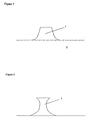
- Another feature of the cross-sectional shape of the grid obtained by the process of the present invention is that the grid has its largest width at the interface with the TCO layer and then tapers off to its smallest cross-section in a curved fashion, e.g, as illustrated in figure 1 , wherein 1 refers to the grid and 2 to the solar cell unit provided with the grid.
- This shape has a number of specific advantages. In the first place, this shape leads to the combination of a relatively high contact area between the grid and the TCO, which leads to less contact resistance losses, and less shadow effect next to the grid. Further, the grid has an increased resistance to delamination because its specific sloping shape ensures a better force dispersion. Finally, the sloping shape makes it easier to apply an encapsulant over the solar cell unit without gas inclusion next to the grid.
- the smallest width of the cross-section of the grid is not necessarily located at the top of the grid. Since the etchant may have a preference for the sideways direction, it may be that the width of the cross-section of the grid is smallest somewhere halfway, as illustrated in figure 2 , wherein 1 refers to the grid and 2 to the solar cell unit provided with the grid. Nevertheless, it is preferred for the grid to have its smallest width of the cross-section at the top of the grid.
- the ratio between the width of the cross-section of the grid at its smallest point and the width of the cross-section at the interface with the TCO generally is between 0.1:1 and 0.9:1, preferably between 0.2:1 and 0.7:1, more preferably between 0.4 and 0.6:1.
- the solar cell unit obtained by the process according to the invention to have at least 50% of its grid surface resulting from the temporary substrate, more preferably at least 70%, still more preferably at least 90%, most preferably at least 95%.
- the temporary substrate is the temporary substrate
- the temporary substrate has to satisfy a number of conditions. It has to be sufficiently conductive to be able to serve as a base material for a current collection grid. It has to be sufficiently heat-resistant to be able to endure the conditions prevailing during the manufacture of the solar cell unit, more particularly during the deposition of the TCO and the PV layer. It has to be strong enough to be able to carry the solar cell unit during its manufacture. It has to be easy to remove from the TCO layer without damaging the latter. The person skilled in the art will be able to select a suitable temporary substrate within these guidelines.
- the temporary substrate employed in the process according to the invention preferably is a foil of a metal or a metal alloy.
- Suitable metals include steel, aluminium, copper, iron, nickel, silver, zinc, molybdenum, chromium, and alloys or multi-layers thereof. For economic reasons among others it is preferred to employ Fe, Al, Cu, or alloys thereof.
- etchants and techniques for removing metals are known, and while they differ per metal, the skilled person will be able to select the appropriate ones.
- Preferred etchants include acids (both Lewis and Br ⁇ nstedt acids).
- acids both Lewis and Br ⁇ nstedt acids.
- FeCl 3 nitric acid or sulphuric acid.
- Suitable etchants for aluminium are, e.g., NaOH, KOH, and mixtures of phosphoric acid and nitric acid.
- copper optionally prepared by way of electrodeposition
- a non-reducing diffusion barrier layer e.g., an anti-corrosion layer, more particularly zinc oxide. This is because copper may have the tendency to diffuse through the TCO layer in the PV layer. It is also possible to select a TCO capable of preventing such diffusion, e.g., SnO 2 or ZnO.
- the anti-diffusion layers can be applied by means of for instance electrodeposition, or via Physical Vapor Deposition (PVD) or via Chemical Vapor Deposition (CVD). The anti-diffusion layer generally is removed from the TCO together with the temporary substrate, but is maintained at the location of the grid.
- the temporary substrate preferably is as thin as possible.
- a certain thickness is required to ensure that the grid obtained from the temporary substrate can collect sufficient current.
- its thickness has to be such that other layers can be provided on it and it has to be able to hold these together, but this generally does not require it to be more than 500 ⁇ m (0.5 mm) thick.
- the thickness preferably is in the range of 1 to 200 ⁇ m (0.2 mm).
- the minimum thickness for a large number of materials will be 5 ⁇ m. Accordingly, a thickness of 5-150 ⁇ m, more particularly 10-100 ⁇ m, is preferred.
- the current collection properties of the grid can be regulated. By varying the width of the etch resist over the surface of the solar cell unit, the current collection properties of the grid can be adapted to the amount of current generated at a specific location.
- TCOs transparent conductive oxides
- suitable transparent conductive oxides are indium tin oxide, zinc oxide, zinc oxide doped with aluminium, fluorine, gallium or boron, cadmium sulphide, cadmium oxide, tin oxide, and, most preferably, F-doped SnO 2 .
- Said last-mentioned transparent electrode material is preferred, because it can form a desired crystalline surface with a columnar light scattering texture when it is applied at a temperature above 400°C, preferably in the range of 500 to 600°C, or after-treated at said temperature. It is precisely in the case of this TCO material that the use of a temporary substrate capable of withstanding such a high temperature is extremely attractive. In addition, the material is resistant to most etchants and has a better resistance to chemicals than the much-used indium tin oxide. Also, it is far less costly.
- the TCO can be applied by means of methods known in the field, e.g., by means of Metal Organic Chemical Vapor Deposition (MOCVD), sputtering, Atmospheric Pressure Chemical Vapor Deposition (APCVD), PECVD, spray pyrolysis, evaporation (physical vapor deposition), electrodeposition, electroless plating, screen printing, sol-gel processes, etc. or combinations of these processes. It is preferred to apply and after-treat the TCO layer at a temperature above 250°C, preferably above 400°C, more preferably between 450 and 600°C, so that a TCO layer of the desired composition, properties and/or texture can be obtained.
- MOCVD Metal Organic Chemical Vapor Deposition
- APCVD Atmospheric Pressure Chemical Vapor Deposition
- PECVD PECVD
- spray pyrolysis evaporation (physical vapor deposition)
- electrodeposition electroless plating
- screen printing sol-gel processes, etc. or combinations of these processes.
- the buffer layer is the buffer layer
- a buffer layer may be present between the TCO layer and the photovoltaic layer.
- the buffer layer is intended to protect the TCO layer from the conditions prevailing during the deposition of the PV layer.
- the nature of the buffer layer will depend on the nature of the PV layer. Suitable buffer layers for the various PV layers are known in the art. For cadmium telluride CdS, In(OH,S) and Zn(OH,S) may be mentioned. If in the present specification mention is made of depositing the PV layer on the TCO, a buffer layer may or may not be present on said TCO.
- the photovoltaic (PV) layer has a photovoltaic (PV) layer
- PV layer After application of the TCO layer the PV layer can be applied in an appropriate manner.
- PV layer or photovoltaic layer comprises the entire system of layers needed to absorb the light and convert it into electricity. Suitable layer configurations are known, as are the methods for applying them. For the common general knowledge in this field reference may be had to Yukinoro Kuwano, "Photovoltaic Cells,” Ullmann's Encyclopedia, Vol.A20 (1992), 161 and “ Solar Technology,” Ullmann's Encyclopedia, Vol.A24 (1993), 369 .
- amorphous silicon a-Si:H
- microcrystalline silicon a-SiC
- amorphous silicon-germanium a-SiGe
- a-SiGe:H amorphous silicon-germanium
- the PV layer in the solar cell unit according to the invention may comprise CIS (copper indium diselenide, CulnSe 2 ), cadmium telluride (CdTe), CIGSS (Cu(In,Ga)(Se,S)), Cu(In,Ga)Se 2 , ZnSe/CIS, ZnO/CIS, and/or Mo/CIS/CdS/ZnO, and dye sensitised solar cells.
- CIS copper indium diselenide, CulnSe 2
- CdTe cadmium telluride
- CIGSS Cu(In,Ga)(Se,S)
- Cu(In,Ga)Se 2 ZnSe/CIS, ZnO/CIS
- Mo/CIS/CdS/ZnO Mo/CIS/CdS/ZnO
- the PV layer preferably is an amorphous silicon layer when the TCO comprises a fluorine-doped tin oxide.
- the PV layer will generally comprise a set, or a plurality of sets, of p-doped, intrinsic, and n-doped amorphous silicon layers, with the p-doped layers being situated on the side receiving the incident light.
- the PV layer will at least comprise a p-doped amorphous silicon layer (Si-p), an intrinsic amorphous silicon layer (Si-i), and an n-doped amorphous silicon layer (Si-n).
- a second and further p-i-n layers are applied onto the first set of p-i-n layers.
- a plurality of repetitive p-i-n (“pinpinpin” or “pinpinpinpin”) layers can be applied consecutively.
- the voltage per cell is raised and the stability of the system is enhanced. Light-induced degradation, the so-called Staebler-Wronski effect, is diminished.
- the spectral response can be optimized by choosing different band-gap materials in the various layers, mainly the i-layers, and particularly within the i-layers.
- the overall thickness of the PV layer, more particularly of all the a-Si layers together, will generally be of the order of 100 to 2,000 nm, more typically about 200 to 600 nm, and preferably about 300 to 500 nm.
- the back electrode in the thin film solar cell sheet according to the invention preferably serves both as reflector and as electrode.
- the back electrode will have a thickness of about 50 to 500 nm, and it may comprise any suitable material having light reflecting properties, preferably aluminium, silver, or a combination of layers of both, and making good ohmic contact with the subjacent semiconductor layer.
- electrodeposition in vacuo
- TiO 2 , TiN, ZnO, and chromium oxide are examples of suitable materials for an adhesion promoter layer and have the advantage of also possessing reflecting properties when applied in a suitable thickness, e.g., of 50-100 nm.
- the required back electrode may be either transparent or opaque.
- the permanent carrier is the permanent carrier
- the solar cell unit Although it is not essential to the process according to the invention, as a rule it is preferred to provide the solar cell unit with a permanent carrier. For, otherwise the unit will be so thin that its fragility makes for difficult handling. When employed, the permanent carrier is applied on the back electrode.
- Suitable carrier layer materials include films of commercially available polymers, such as polyethylene terephthalate, poly(ethylene 2,6-naphthalene dicarboxylate), polycarbonate, polyvinyl chloride, PVDF, PVDC, PPS, PES, PEEK, PEI or films of polymer having very good properties such as aramid or polyimide films, but also, for example, metal foils onto which an insulating (dielectric) surface layer may have been applied, or compositions of plastics and reinforcing fibres and fillers.
- Polymeric" co-extruded” films provided with a thermoplastic adhesive layer having a softening point below that of the substrate itself are preferred.
- the co-extruded film may be provided with an anti-diffusion layer of, e.g., polyester (PET), copolyester or aluminium.
- the thickness of the carrier preferably is 50 ⁇ m to 10 mm. Preferred ranges are 75 ⁇ m to 3 mm and 100 ⁇ m to 300 ⁇ m.
- the bending stiffness of the carrier defined within the context of this description as the product of the modulus of elasticity E in N/mm 2 and the thickness t to the power of three in mm (E x t 3 ), preferably is higher than 16x10 -2 Nmm and will generally be lower than 15x10 6 Nmm.
- the carrier may comprise a structure as required for its final use.
- the substrate may comprise tiles, roofing sheets and elements, façade elements, car and caravan roofs, etc.
- a roll of solar cell foil is obtained which is ready for use and where sheets of the desired power and voltage can be cut off the roll. These can then be incorporated into (hybrid) roof elements or be applied onto tiles, roofing sheets, car and caravan roofs, etc., as desired.
- a top coat or surface layer may be provided on the TCO side of the solar cell to protect the TCO from outside influences.
- the surface layer will be a polymer sheet (with cavities if so desired) or a polymer film.
- the surface layer is required to have a high transmission and for instance comprises the following materials: (per)fluorinated polymers, polycarbonate, poly(methylmethacrylate), PET, PEN or any clear coating available, such as the ones used in the car industry.
- an additional anti-reflection or anti-fouling layer may be provided.
- the entire solar cell may be incorporated into such an encapsulant.
- the etch resist can be any material which can be applied to the temporary substrate in the form of the current collection grid and which will protect the temporary substrate from the action of the etchant.
- suitable material include thermoplastic and thermoset polyurethanes and polyimides, thermoset polymers such as EP, UP, VE, SI, (epoxy)resins, and acrylates, and thermoplastic polymers such as PVC, PI, fluorpolymers, etc.
- the etch resist generally includes additives such as photoinitiators or other hardeners, fillers, plastifiers, etc.
- the etch resist may be temporary, that is, it may be removed at some further stage of the process.
- the etch resist may be permanent.
- the etch resist is suitably applied by vaporising or printing/writing.
- the etch resist is applied by means of a printing process known as such. Suitable printing processes include silk screening, roto screen printing, ink-jet processes, flexgravure, direct extrusion, etc.
- the color of the etch resist can be regulated by the incorporation of suitable pigments or dyes known to the skilled person. Especially for permanent etch resists, the presence of pigments and UV stabilisers may be preferred.
Landscapes
- Photovoltaic Devices (AREA)
Priority Applications (2)
| Application Number | Priority Date | Filing Date | Title |
|---|---|---|---|
| SI200331662T SI1481427T1 (sl) | 2002-03-05 | 2003-03-03 | Postopek za proizvodnjo sonäśne celice kot enote z uporabo zaäśasnega substrata |
| EP03706601A EP1481427B1 (en) | 2002-03-05 | 2003-03-03 | Process for manufacturing a solar cell unit using a temporary substrate |
Applications Claiming Priority (6)
| Application Number | Priority Date | Filing Date | Title |
|---|---|---|---|
| EP02075893 | 2002-03-05 | ||
| EP02075893 | 2002-03-05 | ||
| US36584102P | 2002-03-20 | 2002-03-20 | |
| US365841P | 2002-03-20 | ||
| PCT/EP2003/002218 WO2003075351A2 (en) | 2002-03-05 | 2003-03-03 | Process for manufacturing a solar cell unit using a temporary substrate |
| EP03706601A EP1481427B1 (en) | 2002-03-05 | 2003-03-03 | Process for manufacturing a solar cell unit using a temporary substrate |
Publications (2)
| Publication Number | Publication Date |
|---|---|
| EP1481427A2 EP1481427A2 (en) | 2004-12-01 |
| EP1481427B1 true EP1481427B1 (en) | 2009-08-05 |
Family
ID=35986291
Family Applications (1)
| Application Number | Title | Priority Date | Filing Date |
|---|---|---|---|
| EP03706601A Expired - Lifetime EP1481427B1 (en) | 2002-03-05 | 2003-03-03 | Process for manufacturing a solar cell unit using a temporary substrate |
Country Status (14)
| Country | Link |
|---|---|
| EP (1) | EP1481427B1 (https=) |
| JP (1) | JP4368685B2 (https=) |
| KR (1) | KR100981538B1 (https=) |
| CN (1) | CN100487925C (https=) |
| AT (1) | ATE438930T1 (https=) |
| AU (1) | AU2003208696B2 (https=) |
| BR (1) | BRPI0308218A2 (https=) |
| CA (1) | CA2478109A1 (https=) |
| EA (1) | EA006755B1 (https=) |
| ES (1) | ES2344004T3 (https=) |
| MX (1) | MXPA04008557A (https=) |
| PT (1) | PT1481427E (https=) |
| SI (1) | SI1481427T1 (https=) |
| WO (1) | WO2003075351A2 (https=) |
Families Citing this family (17)
| Publication number | Priority date | Publication date | Assignee | Title |
|---|---|---|---|---|
| DE102004050158B3 (de) | 2004-10-15 | 2006-04-06 | Saint-Gobain Sekurit Deutschland Gmbh & Co. Kg | Transparente Scheibe mit einer beheizbaren Beschichtung |
| US8025929B2 (en) | 2004-11-19 | 2011-09-27 | Helianthos B.V. | Method for preparing flexible mechanically compensated transparent layered material |
| DE102006002636B4 (de) * | 2006-01-19 | 2009-10-22 | Saint-Gobain Sekurit Deutschland Gmbh & Co. Kg | Tansparente Scheibe mit einem beheizbaren Schichtsystem |
| GB0615651D0 (en) | 2006-08-07 | 2006-09-13 | Sun Chemical Bv | A process for manufacturing solar cells |
| EP2093804A1 (en) | 2008-02-19 | 2009-08-26 | Helianthos B.V. | Solar cell system with encapsulant |
| DE102008018147A1 (de) | 2008-04-10 | 2009-10-15 | Saint-Gobain Sekurit Deutschland Gmbh & Co. Kg | Transparente Scheibe mit einer beheizbaren Beschichtung und niederohmigen leitenden Strukturen |
| JP5007907B2 (ja) * | 2008-05-09 | 2012-08-22 | 株式会社豊田中央研究所 | エッチング液及び半導体素子の製造方法 |
| DE202008017877U1 (de) | 2008-07-17 | 2010-10-21 | Saint-Gobain Sekurit Deutschland Gmbh & Co. Kg | Transparente Scheibe mit einer beheizbaren Beschichtung und niederohmigen leitenden Strukturen |
| FR2939239B1 (fr) * | 2008-12-03 | 2010-12-31 | Ecole Polytech | Module photovoltaique comprenant une electrode transparente conductrice d'epaisseur variable et procedes de fabrication d'un tel module |
| KR101206250B1 (ko) | 2009-10-13 | 2012-11-28 | 주식회사 엘지화학 | 식각 마스크 패턴 형성용 페이스트 및 이의 스크린 인쇄법을 이용한 실리콘 태양전지의 제조방법 |
| RU2477905C1 (ru) * | 2011-09-15 | 2013-03-20 | Виктор Анатольевич Капитанов | Тонкопленочный кремниевый фотоэлектрический преобразователь |
| TW201417319A (zh) * | 2012-08-24 | 2014-05-01 | Ind Tech Res Inst | 矽晶太陽能電池及其矽晶太陽能電池模組 |
| JP6048047B2 (ja) * | 2012-10-02 | 2016-12-21 | 凸版印刷株式会社 | 色素増感太陽電池および色素増感太陽電池用光電極 |
| US9502596B2 (en) * | 2013-06-28 | 2016-11-22 | Sunpower Corporation | Patterned thin foil |
| TWI599056B (zh) | 2015-12-28 | 2017-09-11 | 財團法人工業技術研究院 | 太陽能電池 |
| JPWO2019054240A1 (ja) * | 2017-09-15 | 2020-10-15 | 出光興産株式会社 | 光電変換モジュール及び光電変換モジュールを製造する方法 |
| TWI759773B (zh) * | 2020-06-20 | 2022-04-01 | 國立臺灣大學 | 太陽能電池封裝方法與封裝結構 |
Family Cites Families (9)
| Publication number | Priority date | Publication date | Assignee | Title |
|---|---|---|---|---|
| US4262411A (en) * | 1977-09-08 | 1981-04-21 | Photon Power, Inc. | Method of making a solar cell array |
| US4507181A (en) * | 1984-02-17 | 1985-03-26 | Energy Conversion Devices, Inc. | Method of electro-coating a semiconductor device |
| US4771017A (en) * | 1987-06-23 | 1988-09-13 | Spire Corporation | Patterning process |
| US5181968A (en) * | 1991-06-24 | 1993-01-26 | United Solar Systems Corporation | Photovoltaic device having an improved collector grid |
| JP2992638B2 (ja) * | 1995-06-28 | 1999-12-20 | キヤノン株式会社 | 光起電力素子の電極構造及び製造方法並びに太陽電池 |
| EP0931356B1 (en) * | 1996-09-26 | 2004-08-18 | Akzo Nobel N.V. | A photovoltaic foil and method of manufacturing it |
| EP0948004A1 (en) * | 1998-03-26 | 1999-10-06 | Akzo Nobel N.V. | Method for making a photovoltaic cell containing a dye |
| JP4090168B2 (ja) * | 1999-11-30 | 2008-05-28 | 三洋電機株式会社 | 光起電力装置の製造方法 |
| NL1013900C2 (nl) * | 1999-12-21 | 2001-06-25 | Akzo Nobel Nv | Werkwijze voor de vervaardiging van een zonnecelfolie met in serie geschakelde zonnecellen. |
-
2003
- 2003-03-03 WO PCT/EP2003/002218 patent/WO2003075351A2/en not_active Ceased
- 2003-03-03 EA EA200401154A patent/EA006755B1/ru not_active IP Right Cessation
- 2003-03-03 ES ES03706601T patent/ES2344004T3/es not_active Expired - Lifetime
- 2003-03-03 EP EP03706601A patent/EP1481427B1/en not_active Expired - Lifetime
- 2003-03-03 CN CNB038046644A patent/CN100487925C/zh not_active Expired - Lifetime
- 2003-03-03 MX MXPA04008557A patent/MXPA04008557A/es active IP Right Grant
- 2003-03-03 BR BRPI0308218A patent/BRPI0308218A2/pt not_active IP Right Cessation
- 2003-03-03 JP JP2003573704A patent/JP4368685B2/ja not_active Expired - Lifetime
- 2003-03-03 AU AU2003208696A patent/AU2003208696B2/en not_active Ceased
- 2003-03-03 KR KR1020047013834A patent/KR100981538B1/ko not_active Expired - Lifetime
- 2003-03-03 CA CA002478109A patent/CA2478109A1/en not_active Abandoned
- 2003-03-03 PT PT03706601T patent/PT1481427E/pt unknown
- 2003-03-03 SI SI200331662T patent/SI1481427T1/sl unknown
- 2003-03-03 AT AT03706601T patent/ATE438930T1/de active
Also Published As
| Publication number | Publication date |
|---|---|
| WO2003075351A3 (en) | 2003-12-24 |
| BRPI0308218A2 (pt) | 2016-06-21 |
| JP2005519473A (ja) | 2005-06-30 |
| JP4368685B2 (ja) | 2009-11-18 |
| AU2003208696A1 (en) | 2003-09-16 |
| WO2003075351A2 (en) | 2003-09-12 |
| CN100487925C (zh) | 2009-05-13 |
| PT1481427E (pt) | 2009-10-19 |
| EA200401154A1 (ru) | 2005-06-30 |
| ES2344004T3 (es) | 2010-08-16 |
| CN1639880A (zh) | 2005-07-13 |
| KR100981538B1 (ko) | 2010-09-10 |
| MXPA04008557A (es) | 2004-12-06 |
| AU2003208696B2 (en) | 2009-03-26 |
| EA006755B1 (ru) | 2006-04-28 |
| CA2478109A1 (en) | 2003-09-12 |
| KR20040104482A (ko) | 2004-12-10 |
| EP1481427A2 (en) | 2004-12-01 |
| ATE438930T1 (de) | 2009-08-15 |
| SI1481427T1 (sl) | 2009-12-31 |
Similar Documents
| Publication | Publication Date | Title |
|---|---|---|
| US8101851B2 (en) | Process for manufacturing a solar cell foil using a temporary substrate | |
| US6184057B1 (en) | Method of manufacturing a photovoltaic foil | |
| EP1481427B1 (en) | Process for manufacturing a solar cell unit using a temporary substrate | |
| US20010037823A1 (en) | Process for manufacturing a thin film solar cell sheet with solar cells connected in series | |
| EP1273048B1 (en) | Method of manufacturing a photovoltaic foil | |
| US20050109389A1 (en) | Process for manufacturing a solar cell unit using a temporary substrate | |
| EP1866974B1 (en) | Process for manufacturing pieces of a foil having an inorganic coating of e. g. tco | |
| HK1075325A (en) | Process for manufacturing a solar cell unit using a temporary substrate | |
| HK1110994B (en) | Process for manufacturing pieces of a foil having an inorganic coating of e. g. tco and pieces of a foil manufactured by the process | |
| HK1092942A (en) | Process for manufacturing a solar cell foil using a temporary substrate |
Legal Events
| Date | Code | Title | Description |
|---|---|---|---|
| PUAI | Public reference made under article 153(3) epc to a published international application that has entered the european phase |
Free format text: ORIGINAL CODE: 0009012 |
|
| 17P | Request for examination filed |
Effective date: 20040812 |
|
| AK | Designated contracting states |
Kind code of ref document: A2 Designated state(s): AT BE BG CH CY CZ DE DK EE ES FI FR GB GR HU IE IT LI LU MC NL PT RO SE SI SK TR |
|
| AX | Request for extension of the european patent |
Extension state: AL LT LV MK RO |
|
| RIN1 | Information on inventor provided before grant (corrected) |
Inventor name: PETERS, PAULUS, MARINUS, GEZINA, MARIA Inventor name: SCHROPP, RUDOLF, EMMANUEL, ISIDORE Inventor name: MIDDELMAN, ERIK |
|
| RAP1 | Party data changed (applicant data changed or rights of an application transferred) |
Owner name: HELIANTHOS B.V. |
|
| 17Q | First examination report despatched |
Effective date: 20070207 |
|
| GRAP | Despatch of communication of intention to grant a patent |
Free format text: ORIGINAL CODE: EPIDOSNIGR1 |
|
| GRAS | Grant fee paid |
Free format text: ORIGINAL CODE: EPIDOSNIGR3 |
|
| GRAA | (expected) grant |
Free format text: ORIGINAL CODE: 0009210 |
|
| AK | Designated contracting states |
Kind code of ref document: B1 Designated state(s): AT BE BG CH CY CZ DE DK EE ES FI FR GB GR HU IE IT LI LU MC NL PT RO SE SI SK TR |
|
| REG | Reference to a national code |
Ref country code: GB Ref legal event code: FG4D |
|
| REG | Reference to a national code |
Ref country code: CH Ref legal event code: EP |
|
| REG | Reference to a national code |
Ref country code: IE Ref legal event code: FG4D |
|
| REF | Corresponds to: |
Ref document number: 60328665 Country of ref document: DE Date of ref document: 20090917 Kind code of ref document: P |
|
| REG | Reference to a national code |
Ref country code: RO Ref legal event code: EPE Ref country code: PT Ref legal event code: SC4A Free format text: AVAILABILITY OF NATIONAL TRANSLATION Effective date: 20091012 |
|
| REG | Reference to a national code |
Ref country code: GR Ref legal event code: EP Ref document number: 20090402445 Country of ref document: GR |
|
| REG | Reference to a national code |
Ref country code: SK Ref legal event code: T3 Ref document number: E 6133 Country of ref document: SK |
|
| PG25 | Lapsed in a contracting state [announced via postgrant information from national office to epo] |
Ref country code: FI Free format text: LAPSE BECAUSE OF FAILURE TO SUBMIT A TRANSLATION OF THE DESCRIPTION OR TO PAY THE FEE WITHIN THE PRESCRIBED TIME-LIMIT Effective date: 20090805 Ref country code: SE Free format text: LAPSE BECAUSE OF FAILURE TO SUBMIT A TRANSLATION OF THE DESCRIPTION OR TO PAY THE FEE WITHIN THE PRESCRIBED TIME-LIMIT Effective date: 20090805 |
|
| REG | Reference to a national code |
Ref country code: SI Ref legal event code: SP73 Owner name: HELIANTHOS B.V.; NL Effective date: 20091228 |
|
| PG25 | Lapsed in a contracting state [announced via postgrant information from national office to epo] |
Ref country code: EE Free format text: LAPSE BECAUSE OF FAILURE TO SUBMIT A TRANSLATION OF THE DESCRIPTION OR TO PAY THE FEE WITHIN THE PRESCRIBED TIME-LIMIT Effective date: 20090805 Ref country code: DK Free format text: LAPSE BECAUSE OF FAILURE TO SUBMIT A TRANSLATION OF THE DESCRIPTION OR TO PAY THE FEE WITHIN THE PRESCRIBED TIME-LIMIT Effective date: 20090805 |
|
| PLBE | No opposition filed within time limit |
Free format text: ORIGINAL CODE: 0009261 |
|
| STAA | Information on the status of an ep patent application or granted ep patent |
Free format text: STATUS: NO OPPOSITION FILED WITHIN TIME LIMIT |
|
| 26N | No opposition filed |
Effective date: 20100507 |
|
| REG | Reference to a national code |
Ref country code: ES Ref legal event code: FG2A Ref document number: 2344004 Country of ref document: ES Kind code of ref document: T3 |
|
| PG25 | Lapsed in a contracting state [announced via postgrant information from national office to epo] |
Ref country code: MC Free format text: LAPSE BECAUSE OF NON-PAYMENT OF DUE FEES Effective date: 20100331 |
|
| PGFP | Annual fee paid to national office [announced via postgrant information from national office to epo] |
Ref country code: IE Payment date: 20120326 Year of fee payment: 10 |
|
| PGFP | Annual fee paid to national office [announced via postgrant information from national office to epo] |
Ref country code: TR Payment date: 20120228 Year of fee payment: 10 |
|
| PGFP | Annual fee paid to national office [announced via postgrant information from national office to epo] |
Ref country code: GR Payment date: 20120329 Year of fee payment: 10 |
|
| PG25 | Lapsed in a contracting state [announced via postgrant information from national office to epo] |
Ref country code: CY Free format text: LAPSE BECAUSE OF FAILURE TO SUBMIT A TRANSLATION OF THE DESCRIPTION OR TO PAY THE FEE WITHIN THE PRESCRIBED TIME-LIMIT Effective date: 20090805 |
|
| PG25 | Lapsed in a contracting state [announced via postgrant information from national office to epo] |
Ref country code: HU Free format text: LAPSE BECAUSE OF FAILURE TO SUBMIT A TRANSLATION OF THE DESCRIPTION OR TO PAY THE FEE WITHIN THE PRESCRIBED TIME-LIMIT Effective date: 20100206 Ref country code: LU Free format text: LAPSE BECAUSE OF NON-PAYMENT OF DUE FEES Effective date: 20100303 |
|
| PGFP | Annual fee paid to national office [announced via postgrant information from national office to epo] |
Ref country code: CZ Payment date: 20130228 Year of fee payment: 11 Ref country code: RO Payment date: 20130226 Year of fee payment: 11 |
|
| PGFP | Annual fee paid to national office [announced via postgrant information from national office to epo] |
Ref country code: SK Payment date: 20130220 Year of fee payment: 11 Ref country code: SI Payment date: 20130226 Year of fee payment: 11 |
|
| PGFP | Annual fee paid to national office [announced via postgrant information from national office to epo] |
Ref country code: PT Payment date: 20130225 Year of fee payment: 11 Ref country code: AT Payment date: 20130220 Year of fee payment: 11 |
|
| REG | Reference to a national code |
Ref country code: GR Ref legal event code: ML Ref document number: 20090402445 Country of ref document: GR Effective date: 20131002 |
|
| REG | Reference to a national code |
Ref country code: IE Ref legal event code: MM4A |
|
| PG25 | Lapsed in a contracting state [announced via postgrant information from national office to epo] |
Ref country code: IE Free format text: LAPSE BECAUSE OF NON-PAYMENT OF DUE FEES Effective date: 20130303 |
|
| PG25 | Lapsed in a contracting state [announced via postgrant information from national office to epo] |
Ref country code: GR Free format text: LAPSE BECAUSE OF NON-PAYMENT OF DUE FEES Effective date: 20131002 |
|
| PGFP | Annual fee paid to national office [announced via postgrant information from national office to epo] |
Ref country code: BE Payment date: 20140328 Year of fee payment: 12 |
|
| REG | Reference to a national code |
Ref country code: PT Ref legal event code: MM4A Free format text: LAPSE DUE TO NON-PAYMENT OF FEES Effective date: 20140903 |
|
| PG25 | Lapsed in a contracting state [announced via postgrant information from national office to epo] |
Ref country code: CZ Free format text: LAPSE BECAUSE OF NON-PAYMENT OF DUE FEES Effective date: 20140303 Ref country code: RO Free format text: LAPSE BECAUSE OF NON-PAYMENT OF DUE FEES Effective date: 20140303 |
|
| REG | Reference to a national code |
Ref country code: AT Ref legal event code: MM01 Ref document number: 438930 Country of ref document: AT Kind code of ref document: T Effective date: 20140303 |
|
| REG | Reference to a national code |
Ref country code: SK Ref legal event code: MM4A Ref document number: E 6133 Country of ref document: SK Effective date: 20140303 |
|
| PG25 | Lapsed in a contracting state [announced via postgrant information from national office to epo] |
Ref country code: PT Free format text: LAPSE BECAUSE OF NON-PAYMENT OF DUE FEES Effective date: 20140903 |
|
| REG | Reference to a national code |
Ref country code: SI Ref legal event code: KO00 Effective date: 20141104 |
|
| PG25 | Lapsed in a contracting state [announced via postgrant information from national office to epo] |
Ref country code: SK Free format text: LAPSE BECAUSE OF NON-PAYMENT OF DUE FEES Effective date: 20140303 Ref country code: BG Free format text: LAPSE BECAUSE OF NON-PAYMENT OF DUE FEES Effective date: 20141231 |
|
| PG25 | Lapsed in a contracting state [announced via postgrant information from national office to epo] |
Ref country code: AT Free format text: LAPSE BECAUSE OF NON-PAYMENT OF DUE FEES Effective date: 20140303 Ref country code: SI Free format text: LAPSE BECAUSE OF NON-PAYMENT OF DUE FEES Effective date: 20140304 |
|
| PG25 | Lapsed in a contracting state [announced via postgrant information from national office to epo] |
Ref country code: BG Free format text: LAPSE BECAUSE OF NON-PAYMENT OF DUE FEES Effective date: 20140930 |
|
| REG | Reference to a national code |
Ref country code: FR Ref legal event code: PLFP Year of fee payment: 14 |
|
| REG | Reference to a national code |
Ref country code: FR Ref legal event code: PLFP Year of fee payment: 15 |
|
| PG25 | Lapsed in a contracting state [announced via postgrant information from national office to epo] |
Ref country code: BE Free format text: LAPSE BECAUSE OF NON-PAYMENT OF DUE FEES Effective date: 20150331 |
|
| PG25 | Lapsed in a contracting state [announced via postgrant information from national office to epo] |
Ref country code: TR Free format text: LAPSE BECAUSE OF NON-PAYMENT OF DUE FEES Effective date: 20140303 |
|
| PGFP | Annual fee paid to national office [announced via postgrant information from national office to epo] |
Ref country code: BG Payment date: 20130304 Year of fee payment: 11 |
|
| REG | Reference to a national code |
Ref country code: FR Ref legal event code: PLFP Year of fee payment: 16 |
|
| PGFP | Annual fee paid to national office [announced via postgrant information from national office to epo] |
Ref country code: GB Payment date: 20220328 Year of fee payment: 20 Ref country code: DE Payment date: 20220329 Year of fee payment: 20 |
|
| PGFP | Annual fee paid to national office [announced via postgrant information from national office to epo] |
Ref country code: NL Payment date: 20220329 Year of fee payment: 20 Ref country code: IT Payment date: 20220322 Year of fee payment: 20 Ref country code: FR Payment date: 20220325 Year of fee payment: 20 |
|
| PGFP | Annual fee paid to national office [announced via postgrant information from national office to epo] |
Ref country code: ES Payment date: 20220401 Year of fee payment: 20 |
|
| PGFP | Annual fee paid to national office [announced via postgrant information from national office to epo] |
Ref country code: CH Payment date: 20220404 Year of fee payment: 20 |
|
| REG | Reference to a national code |
Ref country code: DE Ref legal event code: R071 Ref document number: 60328665 Country of ref document: DE |
|
| REG | Reference to a national code |
Ref country code: NL Ref legal event code: MK Effective date: 20230302 |
|
| REG | Reference to a national code |
Ref country code: CH Ref legal event code: PL |
|
| REG | Reference to a national code |
Ref country code: GB Ref legal event code: PE20 Expiry date: 20230302 |
|
| REG | Reference to a national code |
Ref country code: ES Ref legal event code: FD2A Effective date: 20230503 |
|
| PG25 | Lapsed in a contracting state [announced via postgrant information from national office to epo] |
Ref country code: GB Free format text: LAPSE BECAUSE OF EXPIRATION OF PROTECTION Effective date: 20230302 |
|
| PG25 | Lapsed in a contracting state [announced via postgrant information from national office to epo] |
Ref country code: ES Free format text: LAPSE BECAUSE OF EXPIRATION OF PROTECTION Effective date: 20230304 |