EP1480345A2 - Stabile Delta-Sigma-Modulatoren hoher Ordnung mit Fehlerrückkopplung und Geräuschübertragsfunktionen zur Anwendung in solchen Modulatoren - Google Patents
Stabile Delta-Sigma-Modulatoren hoher Ordnung mit Fehlerrückkopplung und Geräuschübertragsfunktionen zur Anwendung in solchen Modulatoren Download PDFInfo
- Publication number
- EP1480345A2 EP1480345A2 EP04253046A EP04253046A EP1480345A2 EP 1480345 A2 EP1480345 A2 EP 1480345A2 EP 04253046 A EP04253046 A EP 04253046A EP 04253046 A EP04253046 A EP 04253046A EP 1480345 A2 EP1480345 A2 EP 1480345A2
- Authority
- EP
- European Patent Office
- Prior art keywords
- signal
- modulators
- output
- ntf
- modulator
- Prior art date
- Legal status (The legal status is an assumption and is not a legal conclusion. Google has not performed a legal analysis and makes no representation as to the accuracy of the status listed.)
- Withdrawn
Links
- 238000012546 transfer Methods 0.000 title claims abstract description 25
- 230000006870 function Effects 0.000 title description 14
- 238000000034 method Methods 0.000 claims description 12
- 238000010586 diagram Methods 0.000 description 10
- 238000007493 shaping process Methods 0.000 description 7
- 238000004088 simulation Methods 0.000 description 7
- 238000001228 spectrum Methods 0.000 description 7
- 238000013461 design Methods 0.000 description 6
- 238000013139 quantization Methods 0.000 description 5
- 238000005070 sampling Methods 0.000 description 4
- 230000009286 beneficial effect Effects 0.000 description 3
- 230000001419 dependent effect Effects 0.000 description 3
- 230000004044 response Effects 0.000 description 3
- 238000013112 stability test Methods 0.000 description 3
- 238000012935 Averaging Methods 0.000 description 2
- 101100275990 Drosophila melanogaster Naus gene Proteins 0.000 description 2
- 238000009825 accumulation Methods 0.000 description 2
- 239000000654 additive Substances 0.000 description 2
- 230000000996 additive effect Effects 0.000 description 2
- 230000008901 benefit Effects 0.000 description 2
- 238000006243 chemical reaction Methods 0.000 description 2
- 238000002474 experimental method Methods 0.000 description 2
- 230000007704 transition Effects 0.000 description 2
- 230000003213 activating effect Effects 0.000 description 1
- 239000000872 buffer Substances 0.000 description 1
- 230000008859 change Effects 0.000 description 1
- 230000000052 comparative effect Effects 0.000 description 1
- 230000001934 delay Effects 0.000 description 1
- 230000001627 detrimental effect Effects 0.000 description 1
- 238000007667 floating Methods 0.000 description 1
- 230000006872 improvement Effects 0.000 description 1
- 238000012986 modification Methods 0.000 description 1
- 230000004048 modification Effects 0.000 description 1
- 238000005457 optimization Methods 0.000 description 1
- 230000008569 process Effects 0.000 description 1
- 230000009467 reduction Effects 0.000 description 1
- 230000001629 suppression Effects 0.000 description 1
- 238000012360 testing method Methods 0.000 description 1
- 230000001131 transforming effect Effects 0.000 description 1
Images


Classifications
-
- H—ELECTRICITY
- H03—ELECTRONIC CIRCUITRY
- H03M—CODING; DECODING; CODE CONVERSION IN GENERAL
- H03M7/00—Conversion of a code where information is represented by a given sequence or number of digits to a code where the same, similar or subset of information is represented by a different sequence or number of digits
- H03M7/30—Compression; Expansion; Suppression of unnecessary data, e.g. redundancy reduction
- H03M7/3002—Conversion to or from differential modulation
- H03M7/3004—Digital delta-sigma modulation
- H03M7/3015—Structural details of digital delta-sigma modulators
- H03M7/3031—Structural details of digital delta-sigma modulators characterised by the order of the loop filter, e.g. having a first order loop filter in the feedforward path
- H03M7/3042—Structural details of digital delta-sigma modulators characterised by the order of the loop filter, e.g. having a first order loop filter in the feedforward path the modulator being of the error feedback type, i.e. having loop filter stages in the feedback path only
Definitions
- the present invention concerns delta-sigma error feedback ( ⁇ EF) modulators. More specifically, the present invention concerns noise transfer functions (NTFs) in ⁇ EF modulators, particularly in ⁇ EF modulators used in digital-to-analog converters (DACs) and phase-locked loops (PLLs).
- NTFs noise transfer functions
- DACs digital-to-analog converters
- PLLs phase-locked loops
- Delta-sigma ( ⁇ ) modulators are introduced in ⁇ 1.2.1 below. Then, the use of ⁇ EF modulators in digital-to-analog converters (DACs) and phase-locked loops (PLLs) is introduced in ⁇ 1.2.2. Finally, challenges to designing well-performing ⁇ EF modulators are discussed in ⁇ 1.2.3
- the first mixer 120 includes a first input 122 for accepting an input signal, a second input 124 coupled with an output of the NTF element 130, and an output 126 coupled with an input of the truncation element 120.
- the output 112 of the truncation element 110 is provided as an output.
- the second mixer 140 includes a first input coupled with the output 126 of the first mixer 120, a second input coupled with the output 112 of the truncation element 110, and an output 142 coupled with an input of the NTF element 130.
- the second mixer 140 subtracts higher order bits 112 from the bits 126 to provide lower order bits 142 as its output.
- the truncation element 110 reduces the number of bits in the input signal.
- the ⁇ modulator uses oversampling.
- the NTF element 130 may be used to perform truncation (i.e., quantization) error shaping.
- ⁇ modulator may involve trade-offs between speed and resolution, and analog circuit accuracy and digital circuit complexity.
- ADC analog-to-digital converter
- DAC digital circuit accuracy
- High-order quantization error shaping can be achieved by either single-loop or multi-loop (i.e., cascaded or MASH) architectures.
- single-loop or multi-loop i.e., cascaded or MASH
- MASH multi-loop
- NTF quantization error or quantization noise transfer function
- truncation element (or quantizer) 110 is nonlinear makes a stability analysis of high-order loops a challenge. "Unstable” means that the modulator exhibits large, although not necessarily unbounded, states and a poor SNR compared to those predicted by linear models. (See, e.g., the Norsworthy text, section 4.1.)
- OF modulators used for delta-sigma ADCs and DACs (See, e.g., Figure 2.) may include a chain of integrators or accumulators with feedback or feed-forward summation, respectively.
- a conservative empirical rule See, e.g., W. L. Lee, "A novel higher-order interpolative modulator topology for high resolution oversampling A/D converters," Master's thesis, Massachusetts Institute of Technology, Cambridge, MA, June 1987, incorporated herein by reference and hereafter referred to as "the Lee article”.
- a root-locus method See, e.g., T. Ritoniemi, T.
- Error-feedback (EF) modulators are widely used in ⁇ DACs (See, e.g., the Norsworthy text; H. G. Musmann and W. Korte, "Generalized interpolative method for digital/analog conversion of PCM signals," U.S. Patent 4,467,316, August 21, 1984, incorporated herein by reference and hereafter referred to as "the Musmann patent”; and P. J. Naus, E. C. Dijkmans, E. F. Stikvoort, A. J. McKnight, D. J. Holland, and W. Bradinal, "A CMOS stereo 16-bit D/A converter for digital audio," IEEE J. Solid-State Circuits, vol. 22, no. 3, pp.
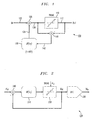
- Figure 3A is a block diagram of a DAC 300 including ⁇ EF modulator 390, such as the one 100 illustrated in Figure 1, and an analog DAC 350.
- the ⁇ EF modulator 390 is used to shape quantization (i.e., truncation) noise. It may be desired to have the analog DAC 350 process less bits so that (i) a more simple circuit may be used, and/or (ii) the analog DAC 350 has better linearity (with respect to frequency).
- the EF modulator 390 includes a first mixing element 320, a truncation element 310, a second mixing element 340 and an NTF element 330.
- NTF elements e.g., loop filters
- internal limiters are often used to protect the overflow of the internal signals.
- the stability of the design is generally carefully verified by extensive simulations.
- stable ⁇ modulators are needed. It might be beneficial if such ⁇ modulators could be provided with a larger, or unbounded input signal. It might be beneficial if techniques for ensuring stability did not come at the expense of in-band noise and resolution, such as occurs when reducing OBG. It might be beneficial to provide a stable ⁇ modulator with a higher order NTF. In summary, better ⁇ modulators would be useful, and could be used to improve devices that use ⁇ modulators such as DACs and PLLs for example.
- ⁇ EF modulators such as those used in digital-to-analog converters and phase-locked loops
- NTF L-order noise transfer function
- the stability of such ⁇ EF modulators is independent of the input signal.
- the out-of-band gain of the NTF is not limited.
- the L is at least four. In at least some embodiments consistent with the present invention, L is 4 or 5.
- Figure 1 is a block diagram of an exemplary ⁇ EF modulator consistent with the present invention.
- Figure 2 is a block diagram of an exemplary ⁇ OF DAC.
- Figures 3A and 3B are block and functional diagrams, respectively, of an exemplary ⁇ EF DAC consistent with the present invention.
- FFT fast Fourier transform
- Figure 6 is a simulated stability test comparing ⁇ EF and OF modulators.
- Figure 7 is a graph illustrating potential performance for various modulators.
- Figure 8 is a block diagram of an experimental 4 th order, 5-bit ⁇ EF DAC, consistent with the present invention.
- Figure 9 is a block diagram of an exemplary ⁇ EF modulator that may be used in the ⁇ EF DAC of Figure 8.
- Figure 10 is a schematic of an exemplary scrambler that may be used in the ⁇ EF DAC of Figure 8.
- Figure 11 is a schematic diagram of an exemplary analog DAC that may be used in the experimental ⁇ EF DAC of Figure 8.
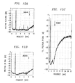
- Figure 12c is a full spectrum version of the device measured in Figure 12b, but with an increased resolution bandwidth.
- the present invention may involve novel methods and/or apparatus for providing stable ⁇ EF modulators.
- the following description is presented to enable one skilled in the art to make and use the invention, and is provided in the context of particular applications and their requirements.
- the following description of embodiments consistent with the present invention provides illustration and description, but is not intended to be exhaustive or to limit the present invention to the precise form disclosed.
- Various modifications to the disclosed embodiments will be apparent to those skilled in the art, and the general principles set forth below may be applied to other embodiments and applications.
- a series of acts may be described, the order of acts may differ in other implementations when the performance of one act is not dependent on the completion of another act. Further, non-dependent acts may be performed in parallel.
- the truncation element 310 provides the most-significant bits y d (MSBs) of the input for the following DAC 350.
- the mixer 340 removes the MSBs from the input, and feeds the least-significant bits (LSBs) to the NTF element (e.g., digital loop filter H(z)) 330.
- LSBs least-significant bits
- the fact that the LSBs are provided to the NTF element 330 is illustrated in the simplified functional diagram of Figure 3B.
- the delta-sigma modulator can be described by a linearized model.
- H(z) is also an FIR function for ⁇ EF modulators. (See equation (1).) Consequently, there is no accumulation in H(z) as opposed to the case of OF topologies. The only accumulation occurs during the addition at the input node, but this is directly followed by the truncation operation. Therefore, the bit length of every internal signal can be accurately predicted analytically without the need of numerical analysis.
- FIR finite impulse response
- the NTF element 330 is an FIR loop filter H(z) that adds m bits to the bit length.
- the input summation 320 adds one more bit at most.
- y d should have m+1 bits at least (i.e., 'm' due to H(z), and '1' due to the input summation).
- the input x d has k x bits and the feedback e h has k e bits.
- a sufficient stability criterion for a ⁇ EF modulator can be expressed as follows: an EF modulator with a truncator of m + 1 bits and an FIR loop filter H(z), which contributes to a m-bit increase in the dataflow, is stable.
- NTF(z) should have high-pass characteristics.
- an L th order differentiator (1 - z -1 ) L may be chosen as NTF(z).
- L also determines the order of the delta-sigma loop. All the zeros of this FIR NTF(z) reside at DC. Therefore, OBG is 2 L , which is the maximum possible OBG value for an L th order modulator.
- OBG stays about 2 L , only slightly smaller. Consistent with the present invention, the sufficient stability criterion is also applicable if an infinite impulse response (IIR) NTF(z) is used.
- IIR infinite impulse response
- a ⁇ EF modulator with (1 - z -1 ) L FIR NTF(z) and L+1 bits is stable.
- This stable EF modulator has an OBG of 2 L .
- reducing OBG improves stability. (See, e.g., Section 5.5 of the Norsworthy text.) Therefore, it is plausible to assume that reducing OBG of this modulator by adding finite-valued poles to its NTF(z) (i.e., turning the initially FIR NTF into an IIR filter) does not worsen its stability.
- a stable L th order (L + 1)-bit ⁇ EF modulator is expected for all possible OBG values.
- ⁇ EF DACs consistent with the present invention may require multi-bit digital-to-analog conversion. Since 1-bit DACs are inherently linear, it is usually desired to obtain a single-bit dataflow at the digital output y d . However, highly-linear multi-bit DACs are available (See, e.g., Chap. 8 of the Norsworthy text.). Alternatively, such a high-order modulator may be used in a cascade configuration. (See, e.g., the Musmann patent.)
- NTF may impact the implementation of the present invention (e.g., as a circuit).
- the use of optimized zeroes NTF may necessitate expensive multipliers in a digital circuit implementation of H(z), while implementing pure differentiator NTFs are free of multipliers.
- the design example presented in ⁇ 4.3 below with reference to Figure 9 demonstrates that even optimized-zeroed NTFs can be effectively implemented by simple, multiplier-free digital circuits.
- ⁇ EF modulators may be used in DACs such as those that reduce the number of bits applied to an analog DAC, as illustrated in Figure 3A. Such ⁇ EF modulators may also be used in PLLs, such as those described in the Willingham article.
- Figure 5 shows the output spectrum of a similar 4 th order 5-bit DAC, but designed using an OF topology (Recall Figure 2.).
- the OBG of the NTF had to be limited to 3.3 to keep the loop stable.
- the z-domain expression of the OF NTF(z) is given by: This modulator achieved 81.2 dB peak SNR, about 12 dB lower than the simulated EF architecture.
- Figure 6 compares the achievable performance of two 4 th order 5-bit optimized-zeroed EF and OF modulators. It shows the peak SNR and the corresponding input signal amplitude A u as a function of OBG. As shown, the OF modulator's performance abruptly drops when OBG > 3.6. The graph indicates that such an OF system cannot sustain stable operation for OBG > 4.1 at all. Note that high OBG OF modulators become unstable if the input signal includes sharp transitions. Even if the input signal is band-limited, the OF modulator can become unstable during start-up and it might not recover.
- the EF modulator remains stable for the whole possible range of OBG with a small decrease of the available input range to about 0.7 V/V (normalized to full scale) as shown.
- EF modulators are insensitive to sharp transitions in the input signal and to start-up conditions.
- the best SNR scenarios for these two 4 th order 5-bit optimized-zeroed EF and OF modulators were shown in Figures 4 and 5, respectively.
- the graph of Figure 7 shows the comparative peak SNR values for EF and OF modulators of various orders with optimized zeros.
- the simulations indicate that the performance of the DC-zeroed OF modulator is only better than that of an optimized-zeroed DF modulator at higher orders (e.g., L ⁇ 5).
- the EF modulator clearly outperforms the OF modulator, since the performance of the OF modulator is limited by the loop's fragile stability.
- a 4 th order 5-bit ⁇ EF DAC prototype consistent with the present invention, was built from discrete components. This prototype was used to experimentally verify the simulation results related to the stability of the high-order loop and to investigate possible detrimental effects of analog circuit imperfections in the multi-bit DAC.
- the prototype 800 includes a digital (e.g., sinusoidal) signal generator 810, a ⁇ EF modulator 820, a scrambler 830, and a DAC (e.g., an analog DAC) 840.
- the ⁇ EF modulator 820 has a 24-bit input x d (provided by the digital sinusoidal generator 810) and a 5-bit output y d .
- the output y d is scrambled by scrambler 830 which generates signal y s .
- the signal y s is then converted into an analog signal y a by a 32-element (i.e., 5-bit) DAC 840.
- Figure 9 illustrates a digital implementation 900 of an optimized-zeroed 4 th order 5-bit EF modulator that may be used as the modulator 820 of Figure 8.
- the approximation error of the coefficients is small enough to avoid a significant change of the resulting NTF(z) and only leads to about 0.1 dB SNR penalty.
- the truncator 930 simply splits bits. The five MSBs constitute the output y d , while the 19-LSB truncation error -e t is fed back into the loop filter H(z).
- DWA data-weighted averaging
- FIG 10 is a block diagram of an exemplary DWA scrambler 1000 that may be used as the scrambler 830 in the DAC 800 of Figure 8.
- the DWA scrambler 1000 rotates a thermometer-coded word using a barrel shifter (ROT) 1020.
- a 5-bit register (REG 1 ) 1040 holds a rotation index which is incremented by the output value of each sample y d . Due to the circular nature of the rotator, the index adder truncates its output to 5 bits.
- the last register (REG 2 ) 1030 of the scrambler avoids data-dependent delays in the signal path.
- various digital logic may be implemented using integer arithmetic on an x86 processor.
- digital logic may be implemented using a digital signal processor (DSP), and/or a field programmable gate array (FPGA).
- DSP digital signal processor
- FPGA field programmable gate array
- FIG 11 illustrates an exemplary (analog) DAC 1100 that may be used as the DAC 840 in the system 800 of Figure 8.
- the 32-line thermometer-coded digital output y s is interfaced with the 32-resistor 1110 "analog" DAC using the parallel port of a personal computer (PC) 1120 and eight 8-bit buffers 1130.
- the common node of the resistors 1110 provides the analog output y a of the ⁇ DAC.
- the timing of the circuit is controlled by an accurate external clock (CLK).
- CLK accurate external clock
- the discrete-component experimental setup mimics an integrated IC scenario. (Note that a commercial implementation would likely use integrated circuits rather than chips.)
- the sampling rate of the DAC was limited to 64 kHz by the parallel port of the PC used in the experiment.
- the digital logic is also implemented on a Xilinx Virtex 300 FPGA using A Stream Compiler (ASC) developed at Bell Laboratories.
- ASC Stream Compiler
- the maximum clock rate supported by the FPGA card is 100 MHz. Due to the simplicity of the digital logic and the optimizations performed by ASC, a 70 MHz output sampling rate is obtained running on the Xilinx Virtex 300 FPGA.
- Figure 12(a) shows the in-band output spectrum without using the DWA scrambler 830 (resolution bandwidth (RBW): 30 Hz). Large harmonics and an increased noise floor can be observed, which limit the SNDR to 58.7 dB. As shown in Figure 12(b), by activating the DWA scrambler 830, the harmonic content becomes negligible and the noise floor is significantly lowered (RBW: 30 Hz). The two NTF(z) minima can be clearly seen. A few small in-band spurious tones are present around the second NTF(z) zero due to idle tones of first-order mismatch shaping. These spurs can be reduced, for example, by using second-order mismatch shaping such as that described in Section 8.3 of the Norsworthy text.
- RBW resolution bandwidth
- the present invention eliminates the need of reducing the OBG of the NTF.
- high-order EF modulators consistent with the present invention are stable and generate high-order noise-shaped, multi-bit output.
- the high-order EF modulators consistent with the present invention may be implemented within a single loop and can be made more hardware efficient and to draw less power than MASH topology modulators.
Landscapes
- Engineering & Computer Science (AREA)
- Theoretical Computer Science (AREA)
- Compression, Expansion, Code Conversion, And Decoders (AREA)
- Amplifiers (AREA)
Applications Claiming Priority (2)
| Application Number | Priority Date | Filing Date | Title |
|---|---|---|---|
| US47248803P | 2003-05-22 | 2003-05-22 | |
| US472488P | 2003-05-22 |
Publications (2)
| Publication Number | Publication Date |
|---|---|
| EP1480345A2 true EP1480345A2 (de) | 2004-11-24 |
| EP1480345A3 EP1480345A3 (de) | 2006-03-22 |
Family
ID=33098336
Family Applications (1)
| Application Number | Title | Priority Date | Filing Date |
|---|---|---|---|
| EP04253046A Withdrawn EP1480345A3 (de) | 2003-05-22 | 2004-05-24 | Stabile Delta-Sigma-Modulatoren hoher Ordnung mit Fehlerrückkopplung und Geräuschübertragsfunktionen zur Anwendung in solchen Modulatoren |
Country Status (3)
| Country | Link |
|---|---|
| US (1) | US6888484B2 (de) |
| EP (1) | EP1480345A3 (de) |
| JP (1) | JP4856363B2 (de) |
Cited By (1)
| Publication number | Priority date | Publication date | Assignee | Title |
|---|---|---|---|---|
| CN109635393A (zh) * | 2018-11-30 | 2019-04-16 | 上海芯钛信息科技有限公司 | 一种基于分布式算法的sigma-delta调制器设计方法及系统 |
Families Citing this family (35)
| Publication number | Priority date | Publication date | Assignee | Title |
|---|---|---|---|---|
| US7986932B1 (en) | 2002-11-19 | 2011-07-26 | National Semiconductor Corporation | Fixed point FIR filter with adaptive truncation and clipping and wireless mobile station using same |
| US7187312B2 (en) * | 2004-01-16 | 2007-03-06 | Cirrus Logic, Inc. | Look-ahead delta sigma modulator having an infinite impulse response filter with multiple look-ahead outputs |
| US7170434B2 (en) * | 2004-01-16 | 2007-01-30 | Cirrus Logic, Inc. | Look-ahead delta sigma modulator with quantization using natural and pattern loop filter responses |
| US7196647B2 (en) * | 2004-01-16 | 2007-03-27 | Cirrus Logic, Inc. | Signal processing with look-ahead modulator noise quantization minimization |
| US7084798B2 (en) * | 2004-01-16 | 2006-08-01 | Cirrus Logic, Inc. | Look-ahead delta sigma modulators with quantizer input approximations |
| US7009543B2 (en) * | 2004-01-16 | 2006-03-07 | Cirrus Logic, Inc. | Multiple non-monotonic quantizer regions for noise shaping |
| US7148830B2 (en) * | 2004-01-26 | 2006-12-12 | Cirrus Logic, Inc. | Look-ahead delta sigma modulator with pruning of output candidate vectors using quantization error minimization pruning techniques |
| US7138934B2 (en) * | 2004-01-26 | 2006-11-21 | Cirrus Logic, Inc. | Pattern biasing for look-ahead delta sigma modulators |
| US7081843B2 (en) * | 2004-07-19 | 2006-07-25 | Cirrus Logic, Inc. | Overload protection for look-ahead delta sigma modulators |
| US7577695B2 (en) * | 2004-07-22 | 2009-08-18 | Auburn University | High-order delta-sigma noise shaping in direct digital frequency synthesis |
| EP1624577B1 (de) * | 2004-08-06 | 2008-07-23 | Verigy (Singapore) Pte. Ltd. | Verbesserte Analogsignalerzeugung mittels eines Delta-Sigma Modulators |
| US6956513B1 (en) * | 2004-10-22 | 2005-10-18 | Broadcom Corporation | Error feedback structure for delta-sigma modulators with improved stability |
| US7321324B2 (en) * | 2005-06-30 | 2008-01-22 | Silicon Laboratories Inc. | Unconditionally stable analog-to-digital converter |
| US7425910B1 (en) * | 2006-02-27 | 2008-09-16 | Marvell International Ltd. | Transmitter digital-to-analog converter with noise shaping |
| US9300261B2 (en) * | 2006-03-10 | 2016-03-29 | Nvidia Corporation | Method and apparatus for efficient load biasing |
| US7548178B2 (en) * | 2006-03-10 | 2009-06-16 | Nvidia Corporation | Method and apparatus for ADC size and performance optimization |
| JP4872439B2 (ja) * | 2006-04-21 | 2012-02-08 | 株式会社Ihi | データ補間方法及びデータ補間装置 |
| GB2438657A (en) * | 2006-06-02 | 2007-12-05 | Ubidyne Inc | Sigma delta modulator utilising systolic array |
| US7317411B1 (en) * | 2006-09-21 | 2008-01-08 | Cirrus Logic, Inc. | Delta-sigma modulator having quantizer code pattern detection controlled dither |
| US7986929B2 (en) | 2006-12-08 | 2011-07-26 | Silicon Laboratories Inc. | Providing channel filtering in an automatic frequency control path |
| GB2451474B (en) * | 2007-07-31 | 2012-03-28 | Wolfson Microelectronics Plc | word length reduction circuit |
| GB2451475B (en) * | 2007-07-31 | 2012-01-11 | Wolfson Microelectronics Plc | Frequency synthesizer |
| US7495589B1 (en) * | 2007-09-17 | 2009-02-24 | Texas Instruments Incorporated | Circuit and method for gain error correction in ADC |
| US9276602B1 (en) | 2009-12-16 | 2016-03-01 | Syntropy Systems, Llc | Conversion of a discrete-time quantized signal into a continuous-time, continuously variable signal |
| US9048865B2 (en) | 2009-12-16 | 2015-06-02 | Syntropy Systems, Llc | Conversion of a discrete time quantized signal into a continuous time, continuously variable signal |
| JP5735981B2 (ja) * | 2009-12-16 | 2015-06-17 | シントロピー システムズSyntropy Systems | 離散時間量子化信号の連続時間連続可変信号への変換 |
| US9680497B2 (en) | 2014-03-26 | 2017-06-13 | Syntropy Systems, Llc | Conversion of a discrete-time quantized signal into a continuous-time, continuously variable signal |
| JP5700702B2 (ja) * | 2012-07-18 | 2015-04-15 | 旭化成エレクトロニクス株式会社 | デルタシグマ変調器 |
| CN103701465B (zh) * | 2013-12-02 | 2016-09-21 | 苏州上声电子有限公司 | 一种基于多比特△—σ调制的数字扬声器系统实现方法和装置 |
| JP6228832B2 (ja) * | 2013-12-17 | 2017-11-08 | ルネサスエレクトロニクス株式会社 | デルタシグマ変調器 |
| US20150372805A1 (en) * | 2014-06-23 | 2015-12-24 | Qualcomm Incorporated | Asynchronous pulse modulation for threshold-based signal coding |
| US9685975B2 (en) | 2015-01-29 | 2017-06-20 | Syntropy Systems, Llc | Distributed combiner for parallel discrete-to-linear converters |
| US9853654B2 (en) * | 2015-02-25 | 2017-12-26 | Qualcomm Incorporated | Error-feedback digital-to-analog converter (DAC) |
| US11683624B1 (en) | 2020-05-12 | 2023-06-20 | Qualcomm Technologies, Inc. | Transducer with analog and digital modulators |
| CN116318165B (zh) * | 2023-03-02 | 2025-06-17 | 上海交通大学 | 采用二阶噪声耦合技术的两阶段线性-指数型增量型高分辨率模数转换器 |
Family Cites Families (3)
| Publication number | Priority date | Publication date | Assignee | Title |
|---|---|---|---|---|
| JPS567346B2 (de) * | 1972-10-11 | 1981-02-17 | ||
| DE3021012C2 (de) * | 1980-06-03 | 1985-08-22 | ANT Nachrichtentechnik GmbH, 7150 Backnang | Verallgemeinertes interpolativers Verfahren zur Digital-Analog-Umsetzung von PCM Signalen |
| KR100686421B1 (ko) * | 2002-03-04 | 2007-02-23 | 에스티마이크로일렉트로닉스 엔.브이. | 공진전원변환 및 방법을 위한 코더장치 |
-
2004
- 2004-05-21 US US10/851,790 patent/US6888484B2/en not_active Expired - Lifetime
- 2004-05-21 JP JP2004151328A patent/JP4856363B2/ja not_active Expired - Fee Related
- 2004-05-24 EP EP04253046A patent/EP1480345A3/de not_active Withdrawn
Non-Patent Citations (4)
| Title |
|---|
| ANDERSSON K O ET AL: "Spectral shaping of DAC nonlinearity errors through modulation of expected errors" ISCAS 2001. PROCEEDINGS OF THE 2001 IEEE INTERNATIONAL SYMPOSIUM ON CIRCUITS AND SYSTEMS. SYDNEY, AUSTRALIA, MAY 6 - 9, 2001, IEEE INTERNATIONAL SYMPOSIUM ON CIRCUITS AND SYSTEMS, NEW YORK, NY : IEEE, US, vol. VOL. 1 OF 5, 6 May 2001 (2001-05-06), pages 417-420, XP010541165 ISBN: 0-7803-6685-9 * |
| KISS P ET AL: "Stable high-order delta-sigma DACS" ISCAS'03. PROCEEDINGS OF THE 2003 INTERNATIONAL SYMPOSIUM ON CIRCUITS AND SYSTEMS, vol. 1, 25 May 2003 (2003-05-25), - 28 May 2003 (2003-05-28) pages I-985-I-988, XP002362554 * |
| SCHREIER R ET AL: "Stability tests for single-bit sigma-delta modulators with second-order FIR noise transfer functions" PROCEEDINGS OF THE INTERNATIONAL SYMPOSIUM ON CIRCUITS AND SYSTEMS. SAN DIEGO, MAY 10 - 13, 1992, PROCEEDINGS OF THE INTERNATIONAL SYMPOSIUM ON CIRCUITS AND SYSTEMS. (ISCAS), NEW YORK, IEEE, US, vol. VOL. 4 CONF. 25, 3 May 1992 (1992-05-03), pages 1316-1319, XP010061384 ISBN: 0-7803-0593-0 * |
| WILLINGHAM S ET AL: "An Integrated 2.5GHz /spl Delta/spl sigma/ Frequency Synthesizer with 5/spl mu/s Settling and 2mb/s Closed Loop Modulation" PROCEEDINGS OF THE INTERNATIONAL SYMPOSIUM ON CIRCUITS AND SYSTEMS. SAN DIEGO, 7 February 2000 (2000-02-07), pages 200-201, XP010378857 * |
Cited By (1)
| Publication number | Priority date | Publication date | Assignee | Title |
|---|---|---|---|---|
| CN109635393A (zh) * | 2018-11-30 | 2019-04-16 | 上海芯钛信息科技有限公司 | 一种基于分布式算法的sigma-delta调制器设计方法及系统 |
Also Published As
| Publication number | Publication date |
|---|---|
| US6888484B2 (en) | 2005-05-03 |
| US20040233086A1 (en) | 2004-11-25 |
| JP4856363B2 (ja) | 2012-01-18 |
| EP1480345A3 (de) | 2006-03-22 |
| JP2004350295A (ja) | 2004-12-09 |
Similar Documents
| Publication | Publication Date | Title |
|---|---|---|
| US6888484B2 (en) | Stable high-order delta-sigma error feedback modulators, and noise transfer functions for use in such modulators | |
| US6304608B1 (en) | Multibit sigma-delta converters employing dynamic element matching with reduced baseband tones | |
| Aziz et al. | An overview of sigma-delta converters | |
| Ritoniemi et al. | Design of stable high order 1-bit sigma-delta modulators | |
| US7576671B2 (en) | Mismatch-shaping dynamic element matching systems and methods for multi-bit sigma-delta data converters | |
| Galton | Spectral shaping of circuit errors in digital-to-analog converters | |
| Kiss et al. | Stable high-order delta-sigma digital-to-analog converters | |
| US7432841B1 (en) | Delta-sigma analog-to-digital converter with pipelined multi-bit quantization | |
| US6940438B2 (en) | Method and circuit for reducing quantizer input/output swing in a sigma-delta modulator | |
| EP3297169A1 (de) | Zeitkontinuierlicher kaskadierter sigma-delta-analog-digital-wandler | |
| Fitzgibbon et al. | Hardware reduction in digital delta-sigma modulators via bus-splitting and error masking—Part II: Non-constant input | |
| CN103762980B (zh) | 一种高稳定性噪声抑制增强σδ调制器结构 | |
| CN102379088B (zh) | 通过使用△-∑调制器直接合成rf信号的方法和装置 | |
| Sun et al. | Reduced complexity, high performance digital delta-sigma modulator for fractional-N frequency synthesis | |
| Enuchenko et al. | Digital-to-analog converters based on delta-sigma modulators | |
| Kiss | Adaptive digital compensation of analog circuit imperfections for cascaded delta-sigma analog-to-digital converters | |
| Lindfors et al. | N‐path dynamic element matching for multibit bandpass ΣΔ modulators | |
| Kiss et al. | Stable high-order delta-sigma DACs | |
| Schubert | High Order Delta-Sigma Modulation with Positive Integer Coefficients | |
| Temes | Delta-sigma D/A converters | |
| Fitzgibbon et al. | Hardware reduction in delta-sigma digital-to-analog converters via bus-splitting | |
| Kennedy | Recent advances in the analysis, design and optimization of Digital Delta-Sigma Modulators | |
| Friedman | Oversampled data conversion techniques | |
| Wisland et al. | A new scalable non-feedback/spl Delta//spl Sigma/digital-to-analog converter | |
| Kulka et al. | Implementation of digital sigma-delta modulators for high-resolution audio digital-to-analog converters based on field programmable gate array |
Legal Events
| Date | Code | Title | Description |
|---|---|---|---|
| PUAI | Public reference made under article 153(3) epc to a published international application that has entered the european phase |
Free format text: ORIGINAL CODE: 0009012 |
|
| AK | Designated contracting states |
Kind code of ref document: A2 Designated state(s): AT BE BG CH CY CZ DE DK EE ES FI FR GB GR HU IE IT LI LU MC NL PL PT RO SE SI SK TR |
|
| AX | Request for extension of the european patent |
Extension state: AL HR LT LV MK |
|
| PUAL | Search report despatched |
Free format text: ORIGINAL CODE: 0009013 |
|
| AK | Designated contracting states |
Kind code of ref document: A3 Designated state(s): AT BE BG CH CY CZ DE DK EE ES FI FR GB GR HU IE IT LI LU MC NL PL PT RO SE SI SK TR |
|
| AX | Request for extension of the european patent |
Extension state: AL HR LT LV MK |
|
| 17P | Request for examination filed |
Effective date: 20060719 |
|
| 17Q | First examination report despatched |
Effective date: 20060823 |
|
| AKX | Designation fees paid |
Designated state(s): DE FR GB |
|
| STAA | Information on the status of an ep patent application or granted ep patent |
Free format text: STATUS: THE APPLICATION IS DEEMED TO BE WITHDRAWN |
|
| 18D | Application deemed to be withdrawn |
Effective date: 20151201 |