EP1480276A1 - Substrat pour dispositif de conversion photoelectrique - Google Patents
Substrat pour dispositif de conversion photoelectrique Download PDFInfo
- Publication number
- EP1480276A1 EP1480276A1 EP02711245A EP02711245A EP1480276A1 EP 1480276 A1 EP1480276 A1 EP 1480276A1 EP 02711245 A EP02711245 A EP 02711245A EP 02711245 A EP02711245 A EP 02711245A EP 1480276 A1 EP1480276 A1 EP 1480276A1
- Authority
- EP
- European Patent Office
- Prior art keywords
- film
- photoelectric conversion
- substrate
- fine particles
- conversion devices
- Prior art date
- Legal status (The legal status is an assumption and is not a legal conclusion. Google has not performed a legal analysis and makes no representation as to the accuracy of the status listed.)
- Withdrawn
Links
- 238000006243 chemical reaction Methods 0.000 title claims abstract description 51
- 239000000758 substrate Substances 0.000 title claims abstract description 44
- 239000011521 glass Substances 0.000 claims abstract description 57
- 239000010419 fine particle Substances 0.000 claims abstract description 48
- VEXZGXHMUGYJMC-UHFFFAOYSA-M Chloride anion Chemical compound [Cl-] VEXZGXHMUGYJMC-UHFFFAOYSA-M 0.000 claims abstract description 25
- 238000009826 distribution Methods 0.000 claims description 9
- 239000005329 float glass Substances 0.000 claims description 3
- 238000006124 Pilkington process Methods 0.000 claims description 2
- 239000010408 film Substances 0.000 description 157
- XOLBLPGZBRYERU-UHFFFAOYSA-N tin dioxide Chemical compound O=[Sn]=O XOLBLPGZBRYERU-UHFFFAOYSA-N 0.000 description 36
- VYPSYNLAJGMNEJ-UHFFFAOYSA-N Silicium dioxide Chemical compound O=[Si]=O VYPSYNLAJGMNEJ-UHFFFAOYSA-N 0.000 description 28
- 229910001887 tin oxide Inorganic materials 0.000 description 25
- 230000000052 comparative effect Effects 0.000 description 23
- 239000007789 gas Substances 0.000 description 20
- 229910052814 silicon oxide Inorganic materials 0.000 description 18
- 239000013078 crystal Substances 0.000 description 16
- BLRPTPMANUNPDV-UHFFFAOYSA-N Silane Chemical compound [SiH4] BLRPTPMANUNPDV-UHFFFAOYSA-N 0.000 description 15
- IJGRMHOSHXDMSA-UHFFFAOYSA-N Atomic nitrogen Chemical compound N#N IJGRMHOSHXDMSA-UHFFFAOYSA-N 0.000 description 14
- QVGXLLKOCUKJST-UHFFFAOYSA-N atomic oxygen Chemical compound [O] QVGXLLKOCUKJST-UHFFFAOYSA-N 0.000 description 13
- 239000000463 material Substances 0.000 description 13
- 239000001301 oxygen Substances 0.000 description 13
- 229910052760 oxygen Inorganic materials 0.000 description 13
- 238000005229 chemical vapour deposition Methods 0.000 description 12
- 239000010409 thin film Substances 0.000 description 11
- 230000015572 biosynthetic process Effects 0.000 description 9
- PKKGKUDPKRTKLJ-UHFFFAOYSA-L dichloro(dimethyl)stannane Chemical compound C[Sn](C)(Cl)Cl PKKGKUDPKRTKLJ-UHFFFAOYSA-L 0.000 description 8
- 239000010410 layer Substances 0.000 description 8
- ZAMOUSCENKQFHK-UHFFFAOYSA-N Chlorine atom Chemical compound [Cl] ZAMOUSCENKQFHK-UHFFFAOYSA-N 0.000 description 7
- VGGSQFUCUMXWEO-UHFFFAOYSA-N Ethene Chemical compound C=C VGGSQFUCUMXWEO-UHFFFAOYSA-N 0.000 description 7
- 239000005977 Ethylene Substances 0.000 description 7
- 239000000460 chlorine Substances 0.000 description 7
- 229910052801 chlorine Inorganic materials 0.000 description 7
- 238000000034 method Methods 0.000 description 7
- 229910052757 nitrogen Inorganic materials 0.000 description 7
- YCKRFDGAMUMZLT-UHFFFAOYSA-N Fluorine atom Chemical compound [F] YCKRFDGAMUMZLT-UHFFFAOYSA-N 0.000 description 6
- XLOMVQKBTHCTTD-UHFFFAOYSA-N Zinc monoxide Chemical compound [Zn]=O XLOMVQKBTHCTTD-UHFFFAOYSA-N 0.000 description 6
- 230000000694 effects Effects 0.000 description 6
- 239000011737 fluorine Substances 0.000 description 6
- 229910052731 fluorine Inorganic materials 0.000 description 6
- 238000004519 manufacturing process Methods 0.000 description 6
- FAPWRFPIFSIZLT-UHFFFAOYSA-M Sodium chloride Chemical compound [Na+].[Cl-] FAPWRFPIFSIZLT-UHFFFAOYSA-M 0.000 description 5
- 239000002245 particle Substances 0.000 description 5
- 230000009257 reactivity Effects 0.000 description 5
- 239000000377 silicon dioxide Substances 0.000 description 5
- 235000012239 silicon dioxide Nutrition 0.000 description 5
- XLYOFNOQVPJJNP-UHFFFAOYSA-N water Chemical compound O XLYOFNOQVPJJNP-UHFFFAOYSA-N 0.000 description 5
- XUIMIQQOPSSXEZ-UHFFFAOYSA-N Silicon Chemical compound [Si] XUIMIQQOPSSXEZ-UHFFFAOYSA-N 0.000 description 4
- 239000011248 coating agent Substances 0.000 description 4
- 238000000576 coating method Methods 0.000 description 4
- 150000001875 compounds Chemical class 0.000 description 4
- 238000007254 oxidation reaction Methods 0.000 description 4
- 229910052710 silicon Inorganic materials 0.000 description 4
- 239000010703 silicon Substances 0.000 description 4
- KRHYYFGTRYWZRS-UHFFFAOYSA-N Fluorane Chemical compound F KRHYYFGTRYWZRS-UHFFFAOYSA-N 0.000 description 3
- BOTDANWDWHJENH-UHFFFAOYSA-N Tetraethyl orthosilicate Chemical compound CCO[Si](OCC)(OCC)OCC BOTDANWDWHJENH-UHFFFAOYSA-N 0.000 description 3
- ATJFFYVFTNAWJD-UHFFFAOYSA-N Tin Chemical compound [Sn] ATJFFYVFTNAWJD-UHFFFAOYSA-N 0.000 description 3
- YXFVVABEGXRONW-UHFFFAOYSA-N Toluene Chemical compound CC1=CC=CC=C1 YXFVVABEGXRONW-UHFFFAOYSA-N 0.000 description 3
- 239000003513 alkali Substances 0.000 description 3
- 229910000040 hydrogen fluoride Inorganic materials 0.000 description 3
- 229910003437 indium oxide Inorganic materials 0.000 description 3
- PJXISJQVUVHSOJ-UHFFFAOYSA-N indium(iii) oxide Chemical compound [O-2].[O-2].[O-2].[In+3].[In+3] PJXISJQVUVHSOJ-UHFFFAOYSA-N 0.000 description 3
- 229910052751 metal Inorganic materials 0.000 description 3
- 230000003647 oxidation Effects 0.000 description 3
- 239000002994 raw material Substances 0.000 description 3
- 239000002210 silicon-based material Substances 0.000 description 3
- 239000002356 single layer Substances 0.000 description 3
- 239000011780 sodium chloride Substances 0.000 description 3
- 235000002639 sodium chloride Nutrition 0.000 description 3
- 239000011787 zinc oxide Substances 0.000 description 3
- AZUYLZMQTIKGSC-UHFFFAOYSA-N 1-[6-[4-(5-chloro-6-methyl-1H-indazol-4-yl)-5-methyl-3-(1-methylindazol-5-yl)pyrazol-1-yl]-2-azaspiro[3.3]heptan-2-yl]prop-2-en-1-one Chemical compound ClC=1C(=C2C=NNC2=CC=1C)C=1C(=NN(C=1C)C1CC2(CN(C2)C(C=C)=O)C1)C=1C=C2C=NN(C2=CC=1)C AZUYLZMQTIKGSC-UHFFFAOYSA-N 0.000 description 2
- CURLTUGMZLYLDI-UHFFFAOYSA-N Carbon dioxide Chemical compound O=C=O CURLTUGMZLYLDI-UHFFFAOYSA-N 0.000 description 2
- GWEVSGVZZGPLCZ-UHFFFAOYSA-N Titan oxide Chemical compound O=[Ti]=O GWEVSGVZZGPLCZ-UHFFFAOYSA-N 0.000 description 2
- DTQVDTLACAAQTR-UHFFFAOYSA-N Trifluoroacetic acid Chemical compound OC(=O)C(F)(F)F DTQVDTLACAAQTR-UHFFFAOYSA-N 0.000 description 2
- HSFWRNGVRCDJHI-UHFFFAOYSA-N alpha-acetylene Natural products C#C HSFWRNGVRCDJHI-UHFFFAOYSA-N 0.000 description 2
- VSCWAEJMTAWNJL-UHFFFAOYSA-K aluminium trichloride Chemical compound Cl[Al](Cl)Cl VSCWAEJMTAWNJL-UHFFFAOYSA-K 0.000 description 2
- YMLFYGFCXGNERH-UHFFFAOYSA-K butyltin trichloride Chemical compound CCCC[Sn](Cl)(Cl)Cl YMLFYGFCXGNERH-UHFFFAOYSA-K 0.000 description 2
- 125000002534 ethynyl group Chemical group [H]C#C* 0.000 description 2
- 230000008018 melting Effects 0.000 description 2
- 238000002844 melting Methods 0.000 description 2
- 239000002184 metal Substances 0.000 description 2
- TWNQGVIAIRXVLR-UHFFFAOYSA-N oxo(oxoalumanyloxy)alumane Chemical compound O=[Al]O[Al]=O TWNQGVIAIRXVLR-UHFFFAOYSA-N 0.000 description 2
- HPGGPRDJHPYFRM-UHFFFAOYSA-J tin(iv) chloride Chemical compound Cl[Sn](Cl)(Cl)Cl HPGGPRDJHPYFRM-UHFFFAOYSA-J 0.000 description 2
- OGIDPMRJRNCKJF-UHFFFAOYSA-N titanium oxide Inorganic materials [Ti]=O OGIDPMRJRNCKJF-UHFFFAOYSA-N 0.000 description 2
- 238000011144 upstream manufacturing Methods 0.000 description 2
- JIAARYAFYJHUJI-UHFFFAOYSA-L zinc dichloride Chemical compound [Cl-].[Cl-].[Zn+2] JIAARYAFYJHUJI-UHFFFAOYSA-L 0.000 description 2
- XBIUWALDKXACEA-UHFFFAOYSA-N 3-[bis(2,4-dioxopentan-3-yl)alumanyl]pentane-2,4-dione Chemical compound CC(=O)C(C(C)=O)[Al](C(C(C)=O)C(C)=O)C(C(C)=O)C(C)=O XBIUWALDKXACEA-UHFFFAOYSA-N 0.000 description 1
- MGWGWNFMUOTEHG-UHFFFAOYSA-N 4-(3,5-dimethylphenyl)-1,3-thiazol-2-amine Chemical compound CC1=CC(C)=CC(C=2N=C(N)SC=2)=C1 MGWGWNFMUOTEHG-UHFFFAOYSA-N 0.000 description 1
- 101100165177 Caenorhabditis elegans bath-15 gene Proteins 0.000 description 1
- UGFAIRIUMAVXCW-UHFFFAOYSA-N Carbon monoxide Chemical compound [O+]#[C-] UGFAIRIUMAVXCW-UHFFFAOYSA-N 0.000 description 1
- VOPWNXZWBYDODV-UHFFFAOYSA-N Chlorodifluoromethane Chemical compound FC(F)Cl VOPWNXZWBYDODV-UHFFFAOYSA-N 0.000 description 1
- UFHFLCQGNIYNRP-UHFFFAOYSA-N Hydrogen Chemical compound [H][H] UFHFLCQGNIYNRP-UHFFFAOYSA-N 0.000 description 1
- DGAQECJNVWCQMB-PUAWFVPOSA-M Ilexoside XXIX Chemical compound C[C@@H]1CC[C@@]2(CC[C@@]3(C(=CC[C@H]4[C@]3(CC[C@@H]5[C@@]4(CC[C@@H](C5(C)C)OS(=O)(=O)[O-])C)C)[C@@H]2[C@]1(C)O)C)C(=O)O[C@H]6[C@@H]([C@H]([C@@H]([C@H](O6)CO)O)O)O.[Na+] DGAQECJNVWCQMB-PUAWFVPOSA-M 0.000 description 1
- CBENFWSGALASAD-UHFFFAOYSA-N Ozone Chemical compound [O-][O+]=O CBENFWSGALASAD-UHFFFAOYSA-N 0.000 description 1
- ZLMJMSJWJFRBEC-UHFFFAOYSA-N Potassium Chemical compound [K] ZLMJMSJWJFRBEC-UHFFFAOYSA-N 0.000 description 1
- 229910021627 Tin(IV) chloride Inorganic materials 0.000 description 1
- 229910001514 alkali metal chloride Inorganic materials 0.000 description 1
- 229910052782 aluminium Inorganic materials 0.000 description 1
- XAGFODPZIPBFFR-UHFFFAOYSA-N aluminium Chemical compound [Al] XAGFODPZIPBFFR-UHFFFAOYSA-N 0.000 description 1
- SMZOGRDCAXLAAR-UHFFFAOYSA-N aluminium isopropoxide Chemical compound [Al+3].CC(C)[O-].CC(C)[O-].CC(C)[O-] SMZOGRDCAXLAAR-UHFFFAOYSA-N 0.000 description 1
- 238000000137 annealing Methods 0.000 description 1
- 229910052787 antimony Inorganic materials 0.000 description 1
- WATWJIUSRGPENY-UHFFFAOYSA-N antimony atom Chemical compound [Sb] WATWJIUSRGPENY-UHFFFAOYSA-N 0.000 description 1
- 230000005540 biological transmission Effects 0.000 description 1
- RJCQBQGAPKAMLL-UHFFFAOYSA-N bromotrifluoromethane Chemical compound FC(F)(F)Br RJCQBQGAPKAMLL-UHFFFAOYSA-N 0.000 description 1
- CREMABGTGYGIQB-UHFFFAOYSA-N carbon carbon Chemical compound C.C CREMABGTGYGIQB-UHFFFAOYSA-N 0.000 description 1
- 229910002092 carbon dioxide Inorganic materials 0.000 description 1
- 239000001569 carbon dioxide Substances 0.000 description 1
- 239000011203 carbon fibre reinforced carbon Substances 0.000 description 1
- 229910002091 carbon monoxide Inorganic materials 0.000 description 1
- KOPOQZFJUQMUML-UHFFFAOYSA-N chlorosilane Chemical compound Cl[SiH3] KOPOQZFJUQMUML-UHFFFAOYSA-N 0.000 description 1
- 238000010586 diagram Methods 0.000 description 1
- RJGHQTVXGKYATR-UHFFFAOYSA-L dibutyl(dichloro)stannane Chemical compound CCCC[Sn](Cl)(Cl)CCCC RJGHQTVXGKYATR-UHFFFAOYSA-L 0.000 description 1
- YNLAOSYQHBDIKW-UHFFFAOYSA-M diethylaluminium chloride Chemical compound CC[Al](Cl)CC YNLAOSYQHBDIKW-UHFFFAOYSA-M 0.000 description 1
- JDTCYQUMKGXSMX-UHFFFAOYSA-N dimethyl(methylsilyl)silane Chemical compound C[SiH2][SiH](C)C JDTCYQUMKGXSMX-UHFFFAOYSA-N 0.000 description 1
- UTUAUBOPWUPBCH-UHFFFAOYSA-N dimethylsilylidene(dimethyl)silane Chemical compound C[Si](C)=[Si](C)C UTUAUBOPWUPBCH-UHFFFAOYSA-N 0.000 description 1
- SBOSGIJGEHWBKV-UHFFFAOYSA-L dioctyltin(2+);dichloride Chemical compound CCCCCCCC[Sn](Cl)(Cl)CCCCCCCC SBOSGIJGEHWBKV-UHFFFAOYSA-L 0.000 description 1
- PZPGRFITIJYNEJ-UHFFFAOYSA-N disilane Chemical compound [SiH3][SiH3] PZPGRFITIJYNEJ-UHFFFAOYSA-N 0.000 description 1
- 230000005611 electricity Effects 0.000 description 1
- -1 for instance Chemical class 0.000 description 1
- 238000005816 glass manufacturing process Methods 0.000 description 1
- 239000001257 hydrogen Substances 0.000 description 1
- 229910052739 hydrogen Inorganic materials 0.000 description 1
- 230000001771 impaired effect Effects 0.000 description 1
- 239000012535 impurity Substances 0.000 description 1
- 239000007788 liquid Substances 0.000 description 1
- 238000000691 measurement method Methods 0.000 description 1
- 229910001510 metal chloride Inorganic materials 0.000 description 1
- 150000002739 metals Chemical class 0.000 description 1
- 239000006060 molten glass Substances 0.000 description 1
- JCXJVPUVTGWSNB-UHFFFAOYSA-N nitrogen dioxide Inorganic materials O=[N]=O JCXJVPUVTGWSNB-UHFFFAOYSA-N 0.000 description 1
- 150000002894 organic compounds Chemical class 0.000 description 1
- 229910052700 potassium Inorganic materials 0.000 description 1
- 239000011591 potassium Substances 0.000 description 1
- 230000005855 radiation Effects 0.000 description 1
- 230000000630 rising effect Effects 0.000 description 1
- 238000000926 separation method Methods 0.000 description 1
- 239000005361 soda-lime glass Substances 0.000 description 1
- 229910052708 sodium Inorganic materials 0.000 description 1
- 239000011734 sodium Substances 0.000 description 1
- 238000005507 spraying Methods 0.000 description 1
- LFQCEHFDDXELDD-UHFFFAOYSA-N tetramethyl orthosilicate Chemical compound CO[Si](OC)(OC)OC LFQCEHFDDXELDD-UHFFFAOYSA-N 0.000 description 1
- VXKWYPOMXBVZSJ-UHFFFAOYSA-N tetramethyltin Chemical compound C[Sn](C)(C)C VXKWYPOMXBVZSJ-UHFFFAOYSA-N 0.000 description 1
- 150000003606 tin compounds Chemical class 0.000 description 1
- XJDNKRIXUMDJCW-UHFFFAOYSA-J titanium tetrachloride Chemical compound Cl[Ti](Cl)(Cl)Cl XJDNKRIXUMDJCW-UHFFFAOYSA-J 0.000 description 1
- 238000002834 transmittance Methods 0.000 description 1
- JLTRXTDYQLMHGR-UHFFFAOYSA-N trimethylaluminium Chemical compound C[Al](C)C JLTRXTDYQLMHGR-UHFFFAOYSA-N 0.000 description 1
- VEDJZFSRVVQBIL-UHFFFAOYSA-N trisilane Chemical compound [SiH3][SiH2][SiH3] VEDJZFSRVVQBIL-UHFFFAOYSA-N 0.000 description 1
- 229930195735 unsaturated hydrocarbon Natural products 0.000 description 1
- 239000011592 zinc chloride Substances 0.000 description 1
- 235000005074 zinc chloride Nutrition 0.000 description 1
Images


Classifications
-
- H—ELECTRICITY
- H01—ELECTRIC ELEMENTS
- H01L—SEMICONDUCTOR DEVICES NOT COVERED BY CLASS H10
- H01L31/00—Semiconductor devices sensitive to infrared radiation, light, electromagnetic radiation of shorter wavelength or corpuscular radiation and specially adapted either for the conversion of the energy of such radiation into electrical energy or for the control of electrical energy by such radiation; Processes or apparatus specially adapted for the manufacture or treatment thereof or of parts thereof; Details thereof
- H01L31/02—Details
- H01L31/0216—Coatings
- H01L31/02161—Coatings for devices characterised by at least one potential jump barrier or surface barrier
- H01L31/02167—Coatings for devices characterised by at least one potential jump barrier or surface barrier for solar cells
-
- H—ELECTRICITY
- H01—ELECTRIC ELEMENTS
- H01L—SEMICONDUCTOR DEVICES NOT COVERED BY CLASS H10
- H01L31/00—Semiconductor devices sensitive to infrared radiation, light, electromagnetic radiation of shorter wavelength or corpuscular radiation and specially adapted either for the conversion of the energy of such radiation into electrical energy or for the control of electrical energy by such radiation; Processes or apparatus specially adapted for the manufacture or treatment thereof or of parts thereof; Details thereof
- H01L31/02—Details
- H01L31/0236—Special surface textures
-
- Y—GENERAL TAGGING OF NEW TECHNOLOGICAL DEVELOPMENTS; GENERAL TAGGING OF CROSS-SECTIONAL TECHNOLOGIES SPANNING OVER SEVERAL SECTIONS OF THE IPC; TECHNICAL SUBJECTS COVERED BY FORMER USPC CROSS-REFERENCE ART COLLECTIONS [XRACs] AND DIGESTS
- Y02—TECHNOLOGIES OR APPLICATIONS FOR MITIGATION OR ADAPTATION AGAINST CLIMATE CHANGE
- Y02E—REDUCTION OF GREENHOUSE GAS [GHG] EMISSIONS, RELATED TO ENERGY GENERATION, TRANSMISSION OR DISTRIBUTION
- Y02E10/00—Energy generation through renewable energy sources
- Y02E10/50—Photovoltaic [PV] energy
Definitions
- the present invention relates to a substrate for photoelectric conversion devices, particularly to a substrate for photoelectric conversion devices that includes a conductive film whose surface has concavities and convexities that are effective for improvement in photoelectric conversion efficiency.
- the thin film photoelectric conversion device includes an undercoating film, a transparent conductive film, a photoelectric conversion unit including a photoelectric conversion layer, and a metal film (a back electrode), which are formed sequentially on the surface of a glass sheet.
- a transparent conductive film a tin oxide film formed by a method accompanied by a pyrolytic oxidation reaction of raw materials, such as a chemical vapor deposition method (a CVD method) for example, is used in many cases.
- the undercoating film is provided for preventing an alkali component that is contained in the glass sheet from diffusing into the transparent conductive film, thus preventing the increase in resistance of the transparent conductive film.
- a transparent thin film such as a silicon oxide film is used as the undercoating film.
- the transparent conductive film of the thin film photoelectric conversion device is required to have a high transmittance (i.e. to introduce a larger quantity of light into the photoelectric conversion layer) and a low resistance (i.e. to reduce the loss that is caused in leading out the generated electricity). It has been known that proper concavities and convexities provided for the surface of the transparent conductive film are effective in trapping light in the photoelectric conversion layer.
- the transparent conductive film is a tin oxide film
- its surface shape is affected by the size and shape of tin oxide crystals.
- the tin oxide film is formed to have a crystal plane with a predetermined orientation and thereby the surface shape is optimized.
- the undercoating film is formed as a film with a smooth surface.
- JP62(1987)-44573A discloses a silicon dioxide film with a surface provided with concavities and convexities through the introduction of silicon dioxide particles thereto.
- the silicon dioxide particles are generated by a partial reaction between monosilane and oxygen. Since monosilane has an excessively high reactivity, nitrogen is introduced as a separation gas, which is intended to prevent the monosilane from being oxidized in the above-mentioned reference. As described in the above-mentioned reference, however, even if monosilane is supplied while being separated from oxygen using nitrogen, monosilane reacts with oxygen rapidly in the reaction space.
- the silicon dioxide particles have large diameters, specifically, 100 nm to 400 nm. It has been reported that the silicon dioxide film formed of these particles had convex portions whose radii and heights were as large as about 500 nm and as high as about 300 nm, respectively.
- the present invention is intended to provide a new substrate for photoelectric conversion devices that has a surface provided with concavities and convexities having an effect in improving the light trapping effect in a photoelectric conversion layer.
- a first substrate for photoelectric conversion devices of the present invention includes an undercoating film and a conductive film that are formed sequentially on a glass sheet.
- the first substrate is characterized in that chloride fine particles are present in the undercoating film or at an interface between the undercoating film and the conductive film, and convex portions are formed on the surface of the conductive film above the chloride fine particles.
- a second substrate for photoelectric conversion devices of the present invention includes an undercoating film and a conductive film that are formed sequentially on a glass sheet.
- the second substrate is characterized in that dome-shaped convex portions with diameters of at least 100 nm are formed on the surface of the conductive film.
- dome-shaped convex portions with diameters of at least 100 nm may be formed on the surface of the conductive film as in the second substrate for photoelectric conversion devices.
- FIG. 1 is a cross-sectional view showing one type of the first substrate for photoelectric conversion devices according to the present invention.
- this substrate for photoelectric conversion devices undercoating films (a first undercoating film 2 and a second undercoating film 3) and a transparent conductive film 4 are stacked sequentially on a glass sheet 1.
- Chloride fine particles 5 are present at the interface between the first undercoating film 2 and the second undercoating film 3.
- the chloride fine particles are, for instance, fine particles of alkali metal chloride such as sodium chloride. In this case, they often take shapes reflecting the rock-salt crystal structure as shown in FIG. 1.
- the surface of the transparent conductive film 4 is provided with convex portions 9 formed with the surface locally rising above the fine particles. These convex portions 9 are larger in diameter and higher than the concavities and convexities that are formed along the exposed surfaces of the crystal grains.
- a suitable diameter D 1 of the convex portions 9 is at least 100 nm, particularly about 100 nm to 500 nm.
- the distribution density of the fine particles (that is, the distribution density of the convex portions) is at least 100 pieces per 100 ⁇ m 2 , particularly about 100 to 1000 pieces per 100 ⁇ m 2 .
- Chloride fine particles that have been prepared separately may be supplied by dispersing. However, when they are allowed to be generated during the formation of the first undercoating film, a film having concavities and convexities formed due to the presence of the fine particles can be manufactured efficiently. Specifically, it is convenient that in forming the first undercoating film, using the CVD method employing a coating-film forming gas including chlorine-containing compounds, the chlorine of the chlorine-containing compounds is allowed to react with alkali components (mainly sodium and potassium) that are contained in glass and thereby chloride fine particles are generated. Thus, when the chloride fine particles are allowed to be present in the film that is formed at the same time the chloride fine particles are formed, without being exhausted through an exhausting system, the undercoating film with fine particles present therein as shown in the drawing can be formed efficiently.
- alkali components mainly sodium and potassium
- the glass temperature is maintained at 600°C or higher, for instance, 600°C to 720°C.
- the "glass temperature” is specifically the temperature of the glass sheet or that of a glass ribbon that is formed in a process of manufacturing the glass sheet.
- the ratio of an amount of gas to be exhausted to an amount of gas to be supplied (hereinafter referred to as an "exhaust bias") is adjusted to be high to a degree that prevents impurities from being introduced into the film.
- exhaust bias In order to allow fine particles to be present in the film, however, it is convenient to adjust the exhaust bias to be lower than that in the conventional common range.
- the height from the glass surface to the lower end of a coater that supplies and exhausts gas also affects the behavior of the fine particles considerably. Accordingly, the introduction of the fine particles into the film can be carried out mainly through the adjustments to the exhaust bias and the height of coater.
- the height of coater corresponds to the distance Hbetween a substrate (in this case, a glass ribbon 10 formed in the glass sheet manufacturing process) and a coater 20 as shown in FIG. 4.
- the chloride fine particles 5 are present inside the undercoating films 1 and 2.
- the fine particles may be present in a state of protruding from the undercoating films.
- the chloride fine particles 5 are present at the interface between the first undercoating film 1 and the transparent conductive film 4.
- the number of layers of the undercoating film and transparent conductive film is not limited to that in the type shown in the drawing.
- the first undercoating film 1 contains, as its main component, tin oxide, titanium oxide, indium oxide, or zinc oxide, and may contain minor components such as fluorine, chlorine, or the like. Furthermore, it may contain other metallic elements as minor components and may be, for example, a film made of tin oxide containing silicon.
- the second undercoating film 2 preferably contains, as its main component, silicon oxide or aluminum oxide. Particularly, it is preferable that the second undercoating film is a silicon oxide film.
- undercoating films include films containing, as their main component, oxycarbides or oxynitrides of the metals described above such as, for instance, SiOC.
- the conductive film 3 preferably contains, as its main component, tin oxide, indium oxide doped with tin, or zinc oxide.
- a tin oxide film that is doped with, for instance, fluorine or antimony so as to have improved conductivity is particularly suitable for the conductive film.
- the amounts of elements to be added are not particularly limited.
- a suitable amount of fluorine, however, is 0.05 wt.% to 1 wt.%.
- Preferable thicknesses of the respective films described above are indicated below as examples.
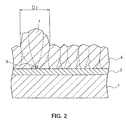
- FIG. 2 is a cross-sectional view showing one type of the second substrate for photoelectric conversion devices according to the present invention.
- this substrate for photoelectric conversion devices an undercoating film 3 and a transparent conductive film 4 are stacked sequentially on a glass sheet 1.
- the surface of the undercoating film i.e. the interface between the undercoating film 3 and the transparent conductive film 4 reflects high smoothness of the glass sheet surface and thus is substantially flat.
- the transparent conductive film 4 has a dome-shaped convex portion 7 on its surface. As shown with broken lines in FIG. 2, a crystal grain that has grown locally abnormally exists inside the dome-shaped convex portion. This convex portion 7 is higher and larger in diameter than the concavities and convexity that are formed along the exposed surface of the crystal grain.
- a suitable diameter D 2 of the convex portion 7 is at least 100 nm, particularly about 100 nm to 500 nm. Furthermore, a preferable distribution density of convex portions (that is, the distribution density of fine particles) is at least 10 pieces per 100 ⁇ m 2 , particularly about 10 to 1000 pieces per 100 ⁇ m 2 . When the size and distribution density of the convex portions are in the ranges mentioned above, a desirable light trapping effect can be obtained.
- the local growth of the crystal grain can be promoted by, for instance, forming a crystalline transparent conductive film 4, with a crystal growth nucleus 6 being present on the surface of the undercoating film 3.
- a minute particle whose diameter is not larger than about 100 nm, more specifically about 5 nm to 40 nm is suitable as the crystal growth nucleus 6. Even if such a minute growth nucleus exists, the flatness of the interface between the undercoating film and the transparent conductive film is not impaired significantly.
- the surface of the undercoating film is considered to be substantially flat as long as it has no concavities nor convexities whose height exceeds 100 nm.
- an undercoating film can be formed that is provided with fine particles exposed thereon as shown in the drawing.
- the coating-film forming gas has excessively high reactivity, it tends to be difficult to generate fine particles having small diameters that are suitable as the crystal growth nuclei.
- an organic gas having a carbon-carbon unsaturated bond such as ethylene or acetylene
- a silicon-containing organic compound such as tetraethyl orthosilicate (TEOS) may be used instead of monosilane.
- a single layer of undercoating film is included.
- a plurality of layers of at least two undercoating films may be formed as in the type shown in FIG. 1.
- Suitable materials for the undercoating film and transparent conductive film are as described above.
- the material suitable for the second undercoating film is used for it.
- the preferable thickness of the single layer of undercoating film is 10 nm to 100 nm.
- a preferable embodiment of the method of manufacturing the above-mentioned substrate for photoelectric conversion devices can be a method of stacking the above-mentioned respective films sequentially on the top surface of a glass ribbon in a float glass manufacturing process using the heat of the glass ribbon.
- the film formation method using heat of the glass ribbon can be a spraying method in which a material liquid is atomized to be supplied onto the glass ribbon surface or the CVD method in which a raw material is vaporized to be supplied onto the glass ribbon surface.
- FIG. 3 shows one type of the apparatus for forming a thin film on the glass ribbon surface by the CVD method in the float glass process.
- a predetermined number of coaters 16 three coaters 16a, 16b, and 16c in the type shown in the drawing
- the glass ribbon 10 is formed from molten glass, which is poured from a melting furnace 11 into a float bath 12 to be formed into a belt-like form on a tin bath 15 while moving thereon.
- the number and arrangement of the coaters may be selected suitably depending on the type and thickness of the coating film to be formed.
- These coaters supply materials, which have been prepared and evaporated, to form coating films on the glass ribbon 10 surface (top surface) successively.
- the first undercoating film, the second undercoating film, and the transparent conductive film can be stacked successively.
- the temperature of the glass ribbon 10 is controlled by a heater and a cooler (not shown in the drawing) installed inside the float bath 12 so that the glass ribbon 10 has a predetermined temperature directly before reaching the coaters 16.
- the predetermined temperature of the glass ribbon is in the range of 600°C to 750°C, particularly 630°C to 750°C.
- the temperature of the glass ribbon 10 may be measured with a radiation thermometer to be controlled.
- the glass ribbon 10 with the coating films thus formed is lifted by a roller 17 and then is annealed in an annealing furnace 13.
- Examples of tin materials that can be used in forming a thin film containing tin oxide as its main component by the CVD method include monobutyltin trichloride, tin tetrachloride, dimethyltin dichloride, dibutyltin dichloride, dioctyltin dichloride, and tetramethyltin.
- Organic tin chlorides such as, for instance, monobutyltin trichloride and dimethyltin dichloride that contain chlorine in a tin compound are particularly suitable when a tin oxide film including chloride fine particles is to be formed.
- Examples of the oxidation material can include oxygen, water vapor, and dry air.
- fluorine material include hydrogen fluoride, trifluoroacetic acid, bromotrifluoromethane, and chlorodifluoromethane.
- a film containing, for instance, titanium oxide, indium oxide, or zinc oxide as its main component may be formed using a chloride-containing material such as metal chloride (for instance, titanium tetrachloride or zinc dichloride) by the CVD method as in the above.
- a chloride-containing material such as metal chloride (for instance, titanium tetrachloride or zinc dichloride)
- Examples of the silicon material to be used in forming a thin film containing silicon oxide as its main component by the CVD method include monosilane, disilane, trisilane, monochlorosilane, 1,2-dimethylsilane, 1,1,2-trimethyldisilane, 1,1,2,2-tetramethyl disilane, tetramethyl orthosilicate, and tetraethyl orthosilicate.
- the oxidation material to be used in this case can be, for example, oxygen, water vapor, dry air, carbon dioxide, carbon monoxide, nitrogen dioxide, or ozone.
- an unsaturated hydrocarbon gas such as ethylene, acetylene, or toluene is added to control the reactivity.
- the aluminum material to be used can be, for instance, trimethylaluminum, aluminum triisopropoxide, diethylaluminum chloride, aluminum acetylacetonate, or aluminum chloride.
- oxygen, water vapor, or dry air can be used as the oxidation material.
- Substrate for Photoelectric Conversion Devices including Chloride Fine Particles
- a film forming gas consisting of dimethyltin dichloride (DMT), oxygen, and nitrogen was supplied from a coater located on the furthest upstream side at a rate of 500 L/min, with the glass ribbon having a surface temperature of 680°C directly before reaching the coater.
- the exhaust bias was set at 1.2 while the height of coater was set at 8 mm.
- a tin oxide film with a thickness of about 23 nm was formed on the top surface of the glass ribbon.
- a mixed gas consisting of monosilane, ethylene, and oxygen was supplied from a coater located downstream.
- the exhaust bias and the height of this coater were set in the ranges that had been used conventionally and were controlled so that even if fine particles of silicon oxide were generated, the film was prevented from including them.
- a mixed gas consisting of dimethyltin dichloride, oxygen, water vapor, nitrogen, and hydrogen fluoride was supplied from a coater located further downstream.
- a silicon oxide film with a thickness of about 25 nm and a SnO 2 :F film with a thickness of about 320 nm were stacked sequentially on the tin oxide film.
- this glass ribbon was cut on a further downstream side and thereby a substrate for photoelectric conversion devices was obtained.
- a substrate for photoelectric conversion devices was obtained in the same manner as in Example 1 except that the glass temperature was set at 580°C when the tin oxide film was formed on the surface of the glass ribbon.
- a substrate for photoelectric conversion devices was obtained in the same manner as in Example 1 except that the exhaust bias was set at 2.0 when the tin oxide film was formed on the surface of the glass ribbon.
- a substrate for photoelectric conversion devices was obtained in the same manner as in Example 1 except that the thickness of the SnO 2 :F film was set at about 600 nm.
- a substrate for photoelectric conversion devices was obtained in the same manner as in Example 2 except that the exhaust bias was set at 2.0 when the tin oxide film was formed on the surface of the glass ribbon.
- the haze ratio can be used as an index of the light trapping effect.
- the increase in thickness of the tin oxide film that is a crystalline coating film causes the increase in size of crystal grains and thus increases the haze ratio.
- Table 1 shows that there were considerable differences in haze ratio between the examples and the comparative examples even when the tin oxide films formed in the examples and the comparative examples had the same thickness.
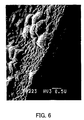
- the surfaces of the thin films (SnO 2 :F films) were observed with the SEM. As a result, it was found that large convex portions were scattered on the film surface in Examples 1 and 2 while being not observed in the comparative examples.
- the glass sheets each were broken so that a portion thereof included the convex portions and the cross-section of the portion was observed with the SEM. As a result, it was confirmed that crystal grains were included in the film and were located below the convex portions. The crystal grains were analyzed and thereby it was confirmed that they consisted substantially of sodium chloride.
- the convex portions had diameters of about 100 nm to 500 nm and heights of about 50 nm to 200 nm.
- the convex portions had a distribution density of about 100 pieces per 100 ⁇ m 2 .
- Comparative Example 1b the glass temperature was too low to generate chloride fine particles from the chlorine-containing compound used therein, while in Comparative Examples 1b and 2, the chloride fine particles were exhausted out of the system swiftly.
- Example 3 and Comparative Example 3 films similarly were formed on a glass ribbon in the same manner as in the above.
- Example 4 and Comparative Example 4 films were formed on a glass sheet. Specific film formation methods are described below.
- a film forming gas consisting of dimethyltin dichloride (DMT), oxygen, and nitrogen was supplied from a coater located on the furthest upstream side, with the glass ribbon having a surface temperature of 650°C directly before reaching the coater.
- DMT dimethyltin dichloride
- oxygen oxygen
- nitrogen nitrogen
- a film forming gas consisting of monosilane, ethylene, and oxygen was supplied from a coater located downstream.
- the exhaust bias was set at 1.2 while the height of coater was set at 12 mm.
- the mole ratio of ethylene to monosilane of the film forming gas was set at 6.
- a silicon oxide film with a thickness of about 25 nm was formed on the tin oxide film.
- Example 2 a mixed gas was supplied from a coater located further downstream to form a SnO 2 :F film with a thickness of about 600 nm in the same manner as in Example 1.
- This glass ribbon was cut on a further downstream side and thereby a substrate for photoelectric conversion devices was obtained.
- a substrate for photoelectric conversion devices was obtained in the same manner as in Example 3 except that the exhaust bias was set at 2.4 and the height of coater was set at 6 mm when the silicon oxide film was formed.
- a 3-mm thick glass sheet that had been precut to have a size of 150 mm ⁇ 150 mm was placed in an belt furnace and was conveyed below a coater while a film forming gas consisting of monosilane, ethylene, and oxygen was supplied from the coater.
- the coater used herein had the same configuration as that shown in FIG. 4.
- the exhaust bias and the height of coater were 1.5 and 25 mm, respectively.
- the mole ratio of ethylene to monosilane of the film forming gas was set at 6.
- a silicon oxide film with a thickness of about 30 nm was formed on the surface of the glass sheet.
- a mixed gas consisting of dimethyltin dichloride, oxygen, water vapor, nitrogen, and hydrogen fluoride was supplied from the coater onto the tin oxide film.
- a substrate for photoelectric conversion devices was obtained with a SnO 2 :F film whose thickness was about 600 nm being formed on the silicon oxide film.
- the temperature of the glass sheet was set at about 600°C in forming both the films described above.
- a substrate for photoelectric conversion devices was obtained in the same manner as in Example 4 except that the exhaust bias was set at 3.1 and the height of coater was set at 13 mm when the silicon oxide film was formed.
- Example 4 a glass sheet having a silicon oxide film alone was produced in the same manner as in Example 4. The surface of this film was observed with the SEM. It was confirmed that fine particles with diameters of about 5 nm to 40 nm were scattered. As the result of analysis, the fine particles were silicon oxide fine particles. On the other hand, such fine particles were not present on the surface of a silicon oxide film formed in the same manner as in Comparative Example 4. In Comparative Example 4 as well as Comparative Example 3, conceivably, the fine particles generated therein were exhausted out of the system swiftly.
- the present invention can provide a substrate for photoelectric conversion devices in which concavities and convexities that can contribute to the light trapping effect of the photoelectric conversion layer are formed. It also is possible to allow the concavities and convexities to be remarkably larger than those obtained through the control of crystal grains.
Applications Claiming Priority (1)
| Application Number | Priority Date | Filing Date | Title |
|---|---|---|---|
| PCT/JP2002/000748 WO2003065461A1 (fr) | 2002-01-31 | 2002-01-31 | Substrat pour dispositif de conversion photoelectrique |
Publications (1)
| Publication Number | Publication Date |
|---|---|
| EP1480276A1 true EP1480276A1 (fr) | 2004-11-24 |
Family
ID=27639271
Family Applications (1)
| Application Number | Title | Priority Date | Filing Date |
|---|---|---|---|
| EP02711245A Withdrawn EP1480276A1 (fr) | 2002-01-31 | 2002-01-31 | Substrat pour dispositif de conversion photoelectrique |
Country Status (3)
| Country | Link |
|---|---|
| US (1) | US20050156167A1 (fr) |
| EP (1) | EP1480276A1 (fr) |
| WO (1) | WO2003065461A1 (fr) |
Families Citing this family (3)
| Publication number | Priority date | Publication date | Assignee | Title |
|---|---|---|---|---|
| CN101477846B (zh) * | 2003-11-18 | 2011-01-12 | 日本板硝子株式会社 | 带有透明导电膜的透明基体及其制造方法、以及含有该基体的光电转换元件 |
| US8613807B2 (en) * | 2009-02-06 | 2013-12-24 | Kabushiki Kaisha Toyota Chuo Kenkyusho | Conductive film, corrosion-resistant conduction film, corrosion-resistant conduction material and process for producing the same |
| US20120237670A1 (en) * | 2011-03-15 | 2012-09-20 | Electronics And Telecommunications Research Institute | Fabricating method of solar cell |
Family Cites Families (9)
| Publication number | Priority date | Publication date | Assignee | Title |
|---|---|---|---|---|
| US5055681A (en) * | 1984-09-18 | 1991-10-08 | Konica Corporation | Radiographic image storage panel and process for reading out a radiographic image |
| JPS6244573A (ja) * | 1985-08-20 | 1987-02-26 | Nippon Sheet Glass Co Ltd | 二酸化珪素含有被膜の製造方法 |
| US4808462A (en) * | 1987-05-22 | 1989-02-28 | Glasstech Solar, Inc. | Solar cell substrate |
| JP3607495B2 (ja) * | 1998-03-12 | 2005-01-05 | 三洋電機株式会社 | 凹凸形状を有する結晶性電極の製造方法及び光起電力素子の製造方法 |
| JP3227449B2 (ja) * | 1999-05-28 | 2001-11-12 | 日本板硝子株式会社 | 光電変換装置用基板とその製造方法、およびこれを用いた光電変換装置 |
| JP4430194B2 (ja) * | 1999-05-31 | 2010-03-10 | 日本板硝子株式会社 | 透明積層体およびこれを用いたガラス物品 |
| JP2001060708A (ja) * | 1999-06-18 | 2001-03-06 | Nippon Sheet Glass Co Ltd | 透明積層体およびこれを用いたガラス物品 |
| JP2001060702A (ja) * | 1999-06-18 | 2001-03-06 | Nippon Sheet Glass Co Ltd | 光電変換装置用基板およびこれを用いた光電変換装置 |
| JP4229606B2 (ja) * | 2000-11-21 | 2009-02-25 | 日本板硝子株式会社 | 光電変換装置用基体およびそれを備えた光電変換装置 |
-
2002
- 2002-01-31 US US10/503,027 patent/US20050156167A1/en not_active Abandoned
- 2002-01-31 WO PCT/JP2002/000748 patent/WO2003065461A1/fr not_active Application Discontinuation
- 2002-01-31 EP EP02711245A patent/EP1480276A1/fr not_active Withdrawn
Non-Patent Citations (1)
| Title |
|---|
| See references of WO03065461A1 * |
Also Published As
| Publication number | Publication date |
|---|---|
| WO2003065461A1 (fr) | 2003-08-07 |
| US20050156167A1 (en) | 2005-07-21 |
Similar Documents
| Publication | Publication Date | Title |
|---|---|---|
| EP1473606A1 (fr) | Systeme de reseau de securite, esclave de securite, et procede de communication | |
| EP1036774B1 (fr) | Substrat en verre ayant un film conducteur transparent | |
| US6380480B1 (en) | Photoelectric conversion device and substrate for photoelectric conversion device | |
| US7846562B2 (en) | Transparent substrate with transparent conductive film, method of manufacturing the same, and photoelectric conversion element including the substrate | |
| US20080038541A1 (en) | Method of forming thin film, substrate having thin film formed by the method, photoelectric conversion device using the substrate | |
| US7320827B2 (en) | Glass substrate and method of manufacturing the same | |
| US20050266253A1 (en) | Glass sheet with conductive film | |
| WO2002043079A1 (fr) | Film électro-conducteur, procédé de production, substrat ainsi pourvu, et convertisseur photoélectrique | |
| EP1480276A1 (fr) | Substrat pour dispositif de conversion photoelectrique | |
| JP2001036117A (ja) | 光電変換装置用基板 | |
| JP4362273B2 (ja) | 基板の製造方法 | |
| EP1419997A1 (fr) | Verre a faible emissivite et procede de production de celui-ci | |
| JP2005029464A (ja) | 薄膜付きガラス板とその製造方法、およびこのガラス板を用いた光電変換装置 | |
| US20050144981A1 (en) | Method of manufacturing glass sheet with thin film and the glass sheet | |
| JP2005029463A (ja) | 透明導電膜付きガラス板とその製造方法、およびこのガラス板を用いた光電変換装置 | |
| WO2003017378A1 (fr) | Substrat utilise dans un dispositif de conversion photoelectrique | |
| JP2000340815A (ja) | 光電変換素子用基板 | |
| JP2002094083A (ja) | 光電変換装置用基板 | |
| JP2002087846A (ja) | 薄膜付きガラス板の製造方法およびそのガラス板 | |
| JP2009239301A (ja) | 基板およびそれを用いた光電変換装置 | |
| JP2001167706A (ja) | ディスプレイ用ガラス基板 | |
| WO2003082759A1 (fr) | Substrat de verre possedant un film mince et procede de fabrication correspondant |
Legal Events
| Date | Code | Title | Description |
|---|---|---|---|
| PUAI | Public reference made under article 153(3) epc to a published international application that has entered the european phase |
Free format text: ORIGINAL CODE: 0009012 |
|
| 17P | Request for examination filed |
Effective date: 20040827 |
|
| AK | Designated contracting states |
Kind code of ref document: A1 Designated state(s): AT BE CH CY DE DK ES FI FR GB GR IE IT LI LU MC NL PT SE TR |
|
| AX | Request for extension of the european patent |
Extension state: AL LT LV MK RO SI |
|
| STAA | Information on the status of an ep patent application or granted ep patent |
Free format text: STATUS: THE APPLICATION HAS BEEN WITHDRAWN |
|
| 18W | Application withdrawn |
Effective date: 20051223 |