EP1480247B1 - Ecran a plasma - Google Patents
Ecran a plasma Download PDFInfo
- Publication number
- EP1480247B1 EP1480247B1 EP03798526A EP03798526A EP1480247B1 EP 1480247 B1 EP1480247 B1 EP 1480247B1 EP 03798526 A EP03798526 A EP 03798526A EP 03798526 A EP03798526 A EP 03798526A EP 1480247 B1 EP1480247 B1 EP 1480247B1
- Authority
- EP
- European Patent Office
- Prior art keywords
- phosphor
- plasma display
- green
- ions
- blue
- Prior art date
- Legal status (The legal status is an assumption and is not a legal conclusion. Google has not performed a legal analysis and makes no representation as to the accuracy of the status listed.)
- Expired - Lifetime
Links
- OAICVXFJPJFONN-UHFFFAOYSA-N Phosphorus Chemical compound [P] OAICVXFJPJFONN-UHFFFAOYSA-N 0.000 claims abstract description 233
- 239000013078 crystal Substances 0.000 claims abstract description 17
- 229910000873 Beta-alumina solid electrolyte Inorganic materials 0.000 claims abstract description 14
- -1 yttrium oxide compound Chemical class 0.000 claims abstract description 11
- 150000002500 ions Chemical class 0.000 claims description 56
- 150000001875 compounds Chemical class 0.000 claims description 30
- 229910052688 Gadolinium Inorganic materials 0.000 claims description 14
- 150000004645 aluminates Chemical class 0.000 claims description 11
- 239000003086 colorant Substances 0.000 claims description 9
- 229910052727 yttrium Inorganic materials 0.000 claims description 7
- SIWVEOZUMHYXCS-UHFFFAOYSA-N oxo(oxoyttriooxy)yttrium Chemical compound O=[Y]O[Y]=O SIWVEOZUMHYXCS-UHFFFAOYSA-N 0.000 claims description 5
- 229910052684 Cerium Inorganic materials 0.000 claims description 4
- 229910052746 lanthanum Inorganic materials 0.000 claims description 4
- 229910052706 scandium Inorganic materials 0.000 claims description 4
- 238000000034 method Methods 0.000 abstract description 70
- 239000012299 nitrogen atmosphere Substances 0.000 abstract description 17
- 238000004519 manufacturing process Methods 0.000 abstract description 15
- 239000007789 gas Substances 0.000 abstract description 11
- 238000001179 sorption measurement Methods 0.000 abstract description 4
- 230000006866 deterioration Effects 0.000 abstract description 3
- 206010021143 Hypoxia Diseases 0.000 abstract 2
- OLBVUFHMDRJKTK-UHFFFAOYSA-N [N].[O] Chemical compound [N].[O] OLBVUFHMDRJKTK-UHFFFAOYSA-N 0.000 abstract 1
- 238000005192 partition Methods 0.000 abstract 1
- 230000000087 stabilizing effect Effects 0.000 abstract 1
- 239000002245 particle Substances 0.000 description 54
- 239000010410 layer Substances 0.000 description 53
- 239000011572 manganese Substances 0.000 description 35
- 239000000523 sample Substances 0.000 description 27
- XLYOFNOQVPJJNP-UHFFFAOYSA-N water Substances O XLYOFNOQVPJJNP-UHFFFAOYSA-N 0.000 description 25
- 239000000203 mixture Substances 0.000 description 24
- 239000000463 material Substances 0.000 description 23
- 239000011521 glass Substances 0.000 description 21
- VYPSYNLAJGMNEJ-UHFFFAOYSA-N Silicium dioxide Chemical compound O=[Si]=O VYPSYNLAJGMNEJ-UHFFFAOYSA-N 0.000 description 20
- 239000012298 atmosphere Substances 0.000 description 20
- 238000003746 solid phase reaction Methods 0.000 description 20
- 229910052844 willemite Inorganic materials 0.000 description 20
- QVGXLLKOCUKJST-UHFFFAOYSA-N atomic oxygen Chemical compound [O] QVGXLLKOCUKJST-UHFFFAOYSA-N 0.000 description 18
- 239000001301 oxygen Substances 0.000 description 18
- 229910052760 oxygen Inorganic materials 0.000 description 18
- 230000015556 catabolic process Effects 0.000 description 17
- 238000006731 degradation reaction Methods 0.000 description 17
- 239000000395 magnesium oxide Substances 0.000 description 17
- CPLXHLVBOLITMK-UHFFFAOYSA-N magnesium oxide Inorganic materials [Mg]=O CPLXHLVBOLITMK-UHFFFAOYSA-N 0.000 description 17
- AXZKOIWUVFPNLO-UHFFFAOYSA-N magnesium;oxygen(2-) Chemical compound [O-2].[Mg+2] AXZKOIWUVFPNLO-UHFFFAOYSA-N 0.000 description 17
- 239000000758 substrate Substances 0.000 description 16
- CURLTUGMZLYLDI-UHFFFAOYSA-N Carbon dioxide Chemical compound O=C=O CURLTUGMZLYLDI-UHFFFAOYSA-N 0.000 description 15
- 229910002651 NO3 Inorganic materials 0.000 description 14
- 238000001027 hydrothermal synthesis Methods 0.000 description 14
- NHNBFGGVMKEFGY-UHFFFAOYSA-N Nitrate Chemical compound [O-][N+]([O-])=O NHNBFGGVMKEFGY-UHFFFAOYSA-N 0.000 description 13
- 239000004215 Carbon black (E152) Substances 0.000 description 12
- 229930195733 hydrocarbon Natural products 0.000 description 12
- 150000002430 hydrocarbons Chemical class 0.000 description 12
- 239000011259 mixed solution Substances 0.000 description 12
- 239000011230 binding agent Substances 0.000 description 11
- UGFAIRIUMAVXCW-UHFFFAOYSA-N Carbon monoxide Chemical compound [O+]#[C-] UGFAIRIUMAVXCW-UHFFFAOYSA-N 0.000 description 10
- 230000004888 barrier function Effects 0.000 description 10
- 239000001569 carbon dioxide Substances 0.000 description 10
- 229910002092 carbon dioxide Inorganic materials 0.000 description 10
- 229910002091 carbon monoxide Inorganic materials 0.000 description 10
- 239000000377 silicon dioxide Substances 0.000 description 10
- 229910052681 coesite Inorganic materials 0.000 description 9
- 229910052906 cristobalite Inorganic materials 0.000 description 9
- 229910052682 stishovite Inorganic materials 0.000 description 9
- 229910052905 tridymite Inorganic materials 0.000 description 9
- 230000000052 comparative effect Effects 0.000 description 8
- 238000002474 experimental method Methods 0.000 description 8
- BASFCYQUMIYNBI-UHFFFAOYSA-N platinum Chemical compound [Pt] BASFCYQUMIYNBI-UHFFFAOYSA-N 0.000 description 8
- 229910052693 Europium Inorganic materials 0.000 description 7
- 239000007864 aqueous solution Substances 0.000 description 7
- KGBXLFKZBHKPEV-UHFFFAOYSA-N boric acid Chemical compound OB(O)O KGBXLFKZBHKPEV-UHFFFAOYSA-N 0.000 description 7
- 230000007423 decrease Effects 0.000 description 7
- YIXJRHPUWRPCBB-UHFFFAOYSA-N magnesium nitrate Chemical compound [Mg+2].[O-][N+]([O-])=O.[O-][N+]([O-])=O YIXJRHPUWRPCBB-UHFFFAOYSA-N 0.000 description 7
- 238000007650 screen-printing Methods 0.000 description 7
- 239000000843 powder Substances 0.000 description 6
- 239000001856 Ethyl cellulose Substances 0.000 description 5
- ZZSNKZQZMQGXPY-UHFFFAOYSA-N Ethyl cellulose Chemical compound CCOCC1OC(OC)C(OCC)C(OCC)C1OC1C(O)C(O)C(OC)C(CO)O1 ZZSNKZQZMQGXPY-UHFFFAOYSA-N 0.000 description 5
- JLDSOYXADOWAKB-UHFFFAOYSA-N aluminium nitrate Chemical compound [Al+3].[O-][N+]([O-])=O.[O-][N+]([O-])=O.[O-][N+]([O-])=O JLDSOYXADOWAKB-UHFFFAOYSA-N 0.000 description 5
- 239000003795 chemical substances by application Substances 0.000 description 5
- 229920001249 ethyl cellulose Polymers 0.000 description 5
- 235000019325 ethyl cellulose Nutrition 0.000 description 5
- GAGGCOKRLXYWIV-UHFFFAOYSA-N europium(3+);trinitrate Chemical compound [Eu+3].[O-][N+]([O-])=O.[O-][N+]([O-])=O.[O-][N+]([O-])=O GAGGCOKRLXYWIV-UHFFFAOYSA-N 0.000 description 5
- 238000011156 evaluation Methods 0.000 description 5
- 229910052748 manganese Inorganic materials 0.000 description 5
- 239000011241 protective layer Substances 0.000 description 5
- 229910052702 rhenium Inorganic materials 0.000 description 5
- 230000002194 synthesizing effect Effects 0.000 description 5
- IJGRMHOSHXDMSA-UHFFFAOYSA-N Atomic nitrogen Chemical compound N#N IJGRMHOSHXDMSA-UHFFFAOYSA-N 0.000 description 4
- YRKCREAYFQTBPV-UHFFFAOYSA-N acetylacetone Chemical compound CC(=O)CC(C)=O YRKCREAYFQTBPV-UHFFFAOYSA-N 0.000 description 4
- PPQREHKVAOVYBT-UHFFFAOYSA-H dialuminum;tricarbonate Chemical compound [Al+3].[Al+3].[O-]C([O-])=O.[O-]C([O-])=O.[O-]C([O-])=O PPQREHKVAOVYBT-UHFFFAOYSA-H 0.000 description 4
- PCHJSUWPFVWCPO-UHFFFAOYSA-N gold Chemical compound [Au] PCHJSUWPFVWCPO-UHFFFAOYSA-N 0.000 description 4
- 229910052737 gold Inorganic materials 0.000 description 4
- 239000010931 gold Substances 0.000 description 4
- 238000005342 ion exchange Methods 0.000 description 4
- 239000005355 lead glass Substances 0.000 description 4
- 238000002156 mixing Methods 0.000 description 4
- 229910052697 platinum Inorganic materials 0.000 description 4
- 238000007789 sealing Methods 0.000 description 4
- 239000002904 solvent Substances 0.000 description 4
- 229910052712 strontium Inorganic materials 0.000 description 4
- OKKJLVBELUTLKV-UHFFFAOYSA-N Methanol Chemical compound OC OKKJLVBELUTLKV-UHFFFAOYSA-N 0.000 description 3
- BQCADISMDOOEFD-UHFFFAOYSA-N Silver Chemical compound [Ag] BQCADISMDOOEFD-UHFFFAOYSA-N 0.000 description 3
- 229910052782 aluminium Inorganic materials 0.000 description 3
- PNEYBMLMFCGWSK-UHFFFAOYSA-N aluminium oxide Inorganic materials [O-2].[O-2].[O-2].[Al+3].[Al+3] PNEYBMLMFCGWSK-UHFFFAOYSA-N 0.000 description 3
- MTHSVFCYNBDYFN-UHFFFAOYSA-N anhydrous diethylene glycol Natural products OCCOCCO MTHSVFCYNBDYFN-UHFFFAOYSA-N 0.000 description 3
- 239000012736 aqueous medium Substances 0.000 description 3
- 238000000889 atomisation Methods 0.000 description 3
- AYJRCSIUFZENHW-UHFFFAOYSA-L barium carbonate Chemical compound [Ba+2].[O-]C([O-])=O AYJRCSIUFZENHW-UHFFFAOYSA-L 0.000 description 3
- IWOUKMZUPDVPGQ-UHFFFAOYSA-N barium nitrate Chemical compound [Ba+2].[O-][N+]([O-])=O.[O-][N+]([O-])=O IWOUKMZUPDVPGQ-UHFFFAOYSA-N 0.000 description 3
- 238000006243 chemical reaction Methods 0.000 description 3
- 230000003247 decreasing effect Effects 0.000 description 3
- 239000002270 dispersing agent Substances 0.000 description 3
- 238000009826 distribution Methods 0.000 description 3
- 239000003779 heat-resistant material Substances 0.000 description 3
- 229910052749 magnesium Inorganic materials 0.000 description 3
- 239000011777 magnesium Substances 0.000 description 3
- 239000011159 matrix material Substances 0.000 description 3
- 239000003960 organic solvent Substances 0.000 description 3
- 230000001590 oxidative effect Effects 0.000 description 3
- 238000000206 photolithography Methods 0.000 description 3
- 239000011347 resin Substances 0.000 description 3
- 229920005989 resin Polymers 0.000 description 3
- 229910052709 silver Inorganic materials 0.000 description 3
- 239000004332 silver Substances 0.000 description 3
- 238000006467 substitution reaction Methods 0.000 description 3
- WUOACPNHFRMFPN-SECBINFHSA-N (S)-(-)-alpha-terpineol Chemical compound CC1=CC[C@@H](C(C)(C)O)CC1 WUOACPNHFRMFPN-SECBINFHSA-N 0.000 description 2
- OAYXUHPQHDHDDZ-UHFFFAOYSA-N 2-(2-butoxyethoxy)ethanol Chemical compound CCCCOCCOCCO OAYXUHPQHDHDDZ-UHFFFAOYSA-N 0.000 description 2
- NGDQQLAVJWUYSF-UHFFFAOYSA-N 4-methyl-2-phenyl-1,3-thiazole-5-sulfonyl chloride Chemical compound S1C(S(Cl)(=O)=O)=C(C)N=C1C1=CC=CC=C1 NGDQQLAVJWUYSF-UHFFFAOYSA-N 0.000 description 2
- 239000004925 Acrylic resin Substances 0.000 description 2
- 229920000178 Acrylic resin Polymers 0.000 description 2
- NLXLAEXVIDQMFP-UHFFFAOYSA-N Ammonia chloride Chemical compound [NH4+].[Cl-] NLXLAEXVIDQMFP-UHFFFAOYSA-N 0.000 description 2
- VHUUQVKOLVNVRT-UHFFFAOYSA-N Ammonium hydroxide Chemical compound [NH4+].[OH-] VHUUQVKOLVNVRT-UHFFFAOYSA-N 0.000 description 2
- LFQSCWFLJHTTHZ-UHFFFAOYSA-N Ethanol Chemical compound CCO LFQSCWFLJHTTHZ-UHFFFAOYSA-N 0.000 description 2
- 150000004703 alkoxides Chemical class 0.000 description 2
- OVKDFILSBMEKLT-UHFFFAOYSA-N alpha-Terpineol Natural products CC(=C)C1(O)CCC(C)=CC1 OVKDFILSBMEKLT-UHFFFAOYSA-N 0.000 description 2
- 229940088601 alpha-terpineol Drugs 0.000 description 2
- 239000000538 analytical sample Substances 0.000 description 2
- 229910052788 barium Inorganic materials 0.000 description 2
- RQPZNWPYLFFXCP-UHFFFAOYSA-L barium dihydroxide Chemical compound [OH-].[OH-].[Ba+2] RQPZNWPYLFFXCP-UHFFFAOYSA-L 0.000 description 2
- 238000005229 chemical vapour deposition Methods 0.000 description 2
- 230000007547 defect Effects 0.000 description 2
- 238000010586 diagram Methods 0.000 description 2
- 238000010304 firing Methods 0.000 description 2
- 238000010438 heat treatment Methods 0.000 description 2
- 239000001257 hydrogen Substances 0.000 description 2
- 229910052739 hydrogen Inorganic materials 0.000 description 2
- 239000012535 impurity Substances 0.000 description 2
- 230000001965 increasing effect Effects 0.000 description 2
- 238000003475 lamination Methods 0.000 description 2
- 238000003754 machining Methods 0.000 description 2
- ZLNQQNXFFQJAID-UHFFFAOYSA-L magnesium carbonate Chemical compound [Mg+2].[O-]C([O-])=O ZLNQQNXFFQJAID-UHFFFAOYSA-L 0.000 description 2
- VTHJTEIRLNZDEV-UHFFFAOYSA-L magnesium dihydroxide Chemical compound [OH-].[OH-].[Mg+2] VTHJTEIRLNZDEV-UHFFFAOYSA-L 0.000 description 2
- 239000000347 magnesium hydroxide Substances 0.000 description 2
- 229910001862 magnesium hydroxide Inorganic materials 0.000 description 2
- MIVBAHRSNUNMPP-UHFFFAOYSA-N manganese(2+);dinitrate Chemical compound [Mn+2].[O-][N+]([O-])=O.[O-][N+]([O-])=O MIVBAHRSNUNMPP-UHFFFAOYSA-N 0.000 description 2
- XMWCXZJXESXBBY-UHFFFAOYSA-L manganese(ii) carbonate Chemical compound [Mn+2].[O-]C([O-])=O XMWCXZJXESXBBY-UHFFFAOYSA-L 0.000 description 2
- 238000005259 measurement Methods 0.000 description 2
- 230000007935 neutral effect Effects 0.000 description 2
- 238000012856 packing Methods 0.000 description 2
- 229910052761 rare earth metal Inorganic materials 0.000 description 2
- 239000000243 solution Substances 0.000 description 2
- UUCCCPNEFXQJEL-UHFFFAOYSA-L strontium dihydroxide Chemical compound [OH-].[OH-].[Sr+2] UUCCCPNEFXQJEL-UHFFFAOYSA-L 0.000 description 2
- 229910001866 strontium hydroxide Inorganic materials 0.000 description 2
- 229910052724 xenon Inorganic materials 0.000 description 2
- BNGXYYYYKUGPPF-UHFFFAOYSA-M (3-methylphenyl)methyl-triphenylphosphanium;chloride Chemical compound [Cl-].CC1=CC=CC(C[P+](C=2C=CC=CC=2)(C=2C=CC=CC=2)C=2C=CC=CC=2)=C1 BNGXYYYYKUGPPF-UHFFFAOYSA-M 0.000 description 1
- LCGLNKUTAGEVQW-UHFFFAOYSA-N Dimethyl ether Chemical compound COC LCGLNKUTAGEVQW-UHFFFAOYSA-N 0.000 description 1
- UFHFLCQGNIYNRP-UHFFFAOYSA-N Hydrogen Chemical compound [H][H] UFHFLCQGNIYNRP-UHFFFAOYSA-N 0.000 description 1
- MXRIRQGCELJRSN-UHFFFAOYSA-N O.O.O.[Al] Chemical compound O.O.O.[Al] MXRIRQGCELJRSN-UHFFFAOYSA-N 0.000 description 1
- WREOTYWODABZMH-DTZQCDIJSA-N [[(2r,3s,4r,5r)-3,4-dihydroxy-5-[2-oxo-4-(2-phenylethoxyamino)pyrimidin-1-yl]oxolan-2-yl]methoxy-hydroxyphosphoryl] phosphono hydrogen phosphate Chemical compound O[C@@H]1[C@H](O)[C@@H](COP(O)(=O)OP(O)(=O)OP(O)(O)=O)O[C@H]1N(C=C\1)C(=O)NC/1=N\OCCC1=CC=CC=C1 WREOTYWODABZMH-DTZQCDIJSA-N 0.000 description 1
- 239000000654 additive Substances 0.000 description 1
- 230000000996 additive effect Effects 0.000 description 1
- 230000032683 aging Effects 0.000 description 1
- 229940118662 aluminum carbonate Drugs 0.000 description 1
- 239000003125 aqueous solvent Substances 0.000 description 1
- 229910001863 barium hydroxide Inorganic materials 0.000 description 1
- QVQLCTNNEUAWMS-UHFFFAOYSA-N barium oxide Inorganic materials [Ba]=O QVQLCTNNEUAWMS-UHFFFAOYSA-N 0.000 description 1
- 150000004649 carbonic acid derivatives Chemical class 0.000 description 1
- 229940125758 compound 15 Drugs 0.000 description 1
- 238000013329 compounding Methods 0.000 description 1
- 229910052593 corundum Inorganic materials 0.000 description 1
- 238000002425 crystallisation Methods 0.000 description 1
- 230000008025 crystallization Effects 0.000 description 1
- 238000003795 desorption Methods 0.000 description 1
- 230000002542 deteriorative effect Effects 0.000 description 1
- 238000007599 discharging Methods 0.000 description 1
- 230000002708 enhancing effect Effects 0.000 description 1
- XZDPDFDAHHNCIW-UHFFFAOYSA-N europium;dihydrate Chemical compound O.O.[Eu] XZDPDFDAHHNCIW-UHFFFAOYSA-N 0.000 description 1
- MWFSXYMZCVAQCC-UHFFFAOYSA-N gadolinium(iii) nitrate Chemical compound [Gd+3].[O-][N+]([O-])=O.[O-][N+]([O-])=O.[O-][N+]([O-])=O MWFSXYMZCVAQCC-UHFFFAOYSA-N 0.000 description 1
- 125000003976 glyceryl group Chemical group [H]C([*])([H])C(O[H])([H])C(O[H])([H])[H] 0.000 description 1
- 230000012447 hatching Effects 0.000 description 1
- 230000036571 hydration Effects 0.000 description 1
- 238000006703 hydration reaction Methods 0.000 description 1
- 150000004679 hydroxides Chemical class 0.000 description 1
- 229910052738 indium Inorganic materials 0.000 description 1
- APFVFJFRJDLVQX-UHFFFAOYSA-N indium atom Chemical compound [In] APFVFJFRJDLVQX-UHFFFAOYSA-N 0.000 description 1
- 239000011261 inert gas Substances 0.000 description 1
- 229910010272 inorganic material Inorganic materials 0.000 description 1
- 239000011147 inorganic material Substances 0.000 description 1
- 229910052747 lanthanoid Inorganic materials 0.000 description 1
- 239000001095 magnesium carbonate Substances 0.000 description 1
- 229910000021 magnesium carbonate Inorganic materials 0.000 description 1
- 239000011656 manganese carbonate Substances 0.000 description 1
- 229910000016 manganese(II) carbonate Inorganic materials 0.000 description 1
- 229910052751 metal Inorganic materials 0.000 description 1
- 239000002184 metal Substances 0.000 description 1
- 239000007769 metal material Substances 0.000 description 1
- 238000003801 milling Methods 0.000 description 1
- 238000002253 near-edge X-ray absorption fine structure spectrum Methods 0.000 description 1
- 229910052754 neon Inorganic materials 0.000 description 1
- GKAOGPIIYCISHV-UHFFFAOYSA-N neon atom Chemical compound [Ne] GKAOGPIIYCISHV-UHFFFAOYSA-N 0.000 description 1
- 150000002823 nitrates Chemical class 0.000 description 1
- 150000004767 nitrides Chemical class 0.000 description 1
- 229910052757 nitrogen Inorganic materials 0.000 description 1
- 150000002902 organometallic compounds Chemical class 0.000 description 1
- 125000002524 organometallic group Chemical group 0.000 description 1
- 239000012071 phase Substances 0.000 description 1
- 229920000642 polymer Polymers 0.000 description 1
- 238000001556 precipitation Methods 0.000 description 1
- 239000005394 sealing glass Substances 0.000 description 1
- 238000005245 sintering Methods 0.000 description 1
- 239000007790 solid phase Substances 0.000 description 1
- 238000004611 spectroscopical analysis Methods 0.000 description 1
- 229910052596 spinel Inorganic materials 0.000 description 1
- 239000011029 spinel Substances 0.000 description 1
- 238000004544 sputter deposition Methods 0.000 description 1
- 239000004094 surface-active agent Substances 0.000 description 1
- 238000012360 testing method Methods 0.000 description 1
- FHNFHKCVQCLJFQ-UHFFFAOYSA-N xenon atom Chemical compound [Xe] FHNFHKCVQCLJFQ-UHFFFAOYSA-N 0.000 description 1
- 229910001845 yogo sapphire Inorganic materials 0.000 description 1
Images


Classifications
-
- H—ELECTRICITY
- H01—ELECTRIC ELEMENTS
- H01J—ELECTRIC DISCHARGE TUBES OR DISCHARGE LAMPS
- H01J29/00—Details of cathode-ray tubes or of electron-beam tubes of the types covered by group H01J31/00
- H01J29/02—Electrodes; Screens; Mounting, supporting, spacing or insulating thereof
- H01J29/10—Screens on or from which an image or pattern is formed, picked up, converted or stored
- H01J29/18—Luminescent screens
- H01J29/26—Luminescent screens with superimposed luminescent layers
-
- H—ELECTRICITY
- H01—ELECTRIC ELEMENTS
- H01J—ELECTRIC DISCHARGE TUBES OR DISCHARGE LAMPS
- H01J11/00—Gas-filled discharge tubes with alternating current induction of the discharge, e.g. alternating current plasma display panels [AC-PDP]; Gas-filled discharge tubes without any main electrode inside the vessel; Gas-filled discharge tubes with at least one main electrode outside the vessel
- H01J11/20—Constructional details
- H01J11/34—Vessels, containers or parts thereof, e.g. substrates
- H01J11/42—Fluorescent layers
-
- C—CHEMISTRY; METALLURGY
- C09—DYES; PAINTS; POLISHES; NATURAL RESINS; ADHESIVES; COMPOSITIONS NOT OTHERWISE PROVIDED FOR; APPLICATIONS OF MATERIALS NOT OTHERWISE PROVIDED FOR
- C09K—MATERIALS FOR MISCELLANEOUS APPLICATIONS, NOT PROVIDED FOR ELSEWHERE
- C09K11/00—Luminescent, e.g. electroluminescent, chemiluminescent materials
- C09K11/08—Luminescent, e.g. electroluminescent, chemiluminescent materials containing inorganic luminescent materials
- C09K11/64—Luminescent, e.g. electroluminescent, chemiluminescent materials containing inorganic luminescent materials containing aluminium
- C09K11/641—Chalcogenides
- C09K11/643—Chalcogenides with alkaline earth metals
-
- C—CHEMISTRY; METALLURGY
- C09—DYES; PAINTS; POLISHES; NATURAL RESINS; ADHESIVES; COMPOSITIONS NOT OTHERWISE PROVIDED FOR; APPLICATIONS OF MATERIALS NOT OTHERWISE PROVIDED FOR
- C09K—MATERIALS FOR MISCELLANEOUS APPLICATIONS, NOT PROVIDED FOR ELSEWHERE
- C09K11/00—Luminescent, e.g. electroluminescent, chemiluminescent materials
- C09K11/08—Luminescent, e.g. electroluminescent, chemiluminescent materials containing inorganic luminescent materials
- C09K11/77—Luminescent, e.g. electroluminescent, chemiluminescent materials containing inorganic luminescent materials containing rare earth metals
- C09K11/7728—Luminescent, e.g. electroluminescent, chemiluminescent materials containing inorganic luminescent materials containing rare earth metals containing europium
- C09K11/7734—Aluminates
-
- C—CHEMISTRY; METALLURGY
- C09—DYES; PAINTS; POLISHES; NATURAL RESINS; ADHESIVES; COMPOSITIONS NOT OTHERWISE PROVIDED FOR; APPLICATIONS OF MATERIALS NOT OTHERWISE PROVIDED FOR
- C09K—MATERIALS FOR MISCELLANEOUS APPLICATIONS, NOT PROVIDED FOR ELSEWHERE
- C09K11/00—Luminescent, e.g. electroluminescent, chemiluminescent materials
- C09K11/08—Luminescent, e.g. electroluminescent, chemiluminescent materials containing inorganic luminescent materials
- C09K11/77—Luminescent, e.g. electroluminescent, chemiluminescent materials containing inorganic luminescent materials containing rare earth metals
- C09K11/7766—Luminescent, e.g. electroluminescent, chemiluminescent materials containing inorganic luminescent materials containing rare earth metals containing two or more rare earth metals
- C09K11/778—Borates
-
- C—CHEMISTRY; METALLURGY
- C09—DYES; PAINTS; POLISHES; NATURAL RESINS; ADHESIVES; COMPOSITIONS NOT OTHERWISE PROVIDED FOR; APPLICATIONS OF MATERIALS NOT OTHERWISE PROVIDED FOR
- C09K—MATERIALS FOR MISCELLANEOUS APPLICATIONS, NOT PROVIDED FOR ELSEWHERE
- C09K11/00—Luminescent, e.g. electroluminescent, chemiluminescent materials
- C09K11/08—Luminescent, e.g. electroluminescent, chemiluminescent materials containing inorganic luminescent materials
- C09K11/77—Luminescent, e.g. electroluminescent, chemiluminescent materials containing inorganic luminescent materials containing rare earth metals
- C09K11/7783—Luminescent, e.g. electroluminescent, chemiluminescent materials containing inorganic luminescent materials containing rare earth metals containing two or more rare earth metals one of which being europium
- C09K11/7784—Chalcogenides
- C09K11/7787—Oxides
-
- C—CHEMISTRY; METALLURGY
- C09—DYES; PAINTS; POLISHES; NATURAL RESINS; ADHESIVES; COMPOSITIONS NOT OTHERWISE PROVIDED FOR; APPLICATIONS OF MATERIALS NOT OTHERWISE PROVIDED FOR
- C09K—MATERIALS FOR MISCELLANEOUS APPLICATIONS, NOT PROVIDED FOR ELSEWHERE
- C09K11/00—Luminescent, e.g. electroluminescent, chemiluminescent materials
- C09K11/08—Luminescent, e.g. electroluminescent, chemiluminescent materials containing inorganic luminescent materials
- C09K11/77—Luminescent, e.g. electroluminescent, chemiluminescent materials containing inorganic luminescent materials containing rare earth metals
- C09K11/7783—Luminescent, e.g. electroluminescent, chemiluminescent materials containing inorganic luminescent materials containing rare earth metals containing two or more rare earth metals one of which being europium
- C09K11/7797—Borates
-
- H—ELECTRICITY
- H01—ELECTRIC ELEMENTS
- H01J—ELECTRIC DISCHARGE TUBES OR DISCHARGE LAMPS
- H01J1/00—Details of electrodes, of magnetic control means, of screens, or of the mounting or spacing thereof, common to two or more basic types of discharge tubes or lamps
- H01J1/54—Screens on or from which an image or pattern is formed, picked-up, converted, or stored; Luminescent coatings on vessels
- H01J1/62—Luminescent screens; Selection of materials for luminescent coatings on vessels
- H01J1/63—Luminescent screens; Selection of materials for luminescent coatings on vessels characterised by the luminescent material
-
- H—ELECTRICITY
- H01—ELECTRIC ELEMENTS
- H01J—ELECTRIC DISCHARGE TUBES OR DISCHARGE LAMPS
- H01J11/00—Gas-filled discharge tubes with alternating current induction of the discharge, e.g. alternating current plasma display panels [AC-PDP]; Gas-filled discharge tubes without any main electrode inside the vessel; Gas-filled discharge tubes with at least one main electrode outside the vessel
- H01J11/10—AC-PDPs with at least one main electrode being out of contact with the plasma
- H01J11/12—AC-PDPs with at least one main electrode being out of contact with the plasma with main electrodes provided on both sides of the discharge space
Definitions
- the present invention relates to a plasma display device that is used for displaying an image on a television (TV) set or other equipment and has phosphor layers exited by ultraviolet light to emit light.
- TV television
- a plasma display device having a plasma display panel (hereinafter referred to as a PDP) has recently received considerable attention as a color display device with large sized screen but lightweight body due to its low-profile structure.
- a plasma display device images in full color by performing an additive color mixing process on red, green, and blue - known as the three primary colors.
- the plasma display device has phosphor layers that are respectively prepared for emitting red (R), green (G), and blue (B) of the three primary colors.
- a phosphor layer is formed of phosphor particles. The phosphor particles are excited by ultraviolet light generated in a discharge cell in the PDP, so that visible light of red, green, and blue are produced.
- a phosphor Zn 2 SiO 4 :Mn 2+ is produced through solid phase reaction.
- specified materials are mixed, and baked at high temperatures of at least 1,000°C (for example, see Phosphor Handbook, pp 219 and 220, Ohmsha ). After the baked phosphor particles are lightly milled so that aggregated particles loosen and breakage of crystals causing luminance degradation does not occur, they are classified so that red and green phosphors have an average particle diameter of 2-5 ⁇ m, and the blue phosphor 3-10 ⁇ m
- the phosphor particles are milled and classified for the following reason.
- a method of screen-printing a paste of phosphor particles of each color, or an ink jet method of discharging a phosphor paste from a nozzle for application is used.
- the smaller and more uniform diameters of phosphor particles i.e. a uniform particle size distribution
- non-uniform application or clogging of a nozzle may occur because large aggregates are included in the phosphors if the particles are not lightly milled and classified (for example, see Japanese Patent Unexamined Publication No.
- the coated surface is smoother.
- the smoother coated surface increases the packing density of the phosphor particles in a phosphor layer. As a result, the emission surface area of the particles increases, and the luminance of the plasma display device increases.
- JP 2000 251701 discloses a display device with a red-green-blue fluorescent layer, wherein the red phosphor can be an yttrium oxide according the formula (Y 1-x EU x ) 2 O 3 ), the green phosphor can be a mixture of an aluminate according the formula (Ba, Sr, Mg)0.5Al 2 O 3 :Mn and YBO 3 :Tb and the blue phosphor may be Ba 1-x Eu x MgAl 10 O 17 .
- the red phosphor can be an yttrium oxide according the formula (Y 1-x EU x ) 2 O 3 )
- the green phosphor can be a mixture of an aluminate according the formula (Ba, Sr, Mg)0.5Al 2 O 3 :Mn and YBO 3 :Tb
- the blue phosphor may be Ba 1-x Eu x MgAl 10 O 17 .
- a plasma display panel produced by using BaMgAl 10 O 17 :Eu as a blue phosphor, Zn 2 SiO 4 :Mn as a green phosphor, and (Y,Gd) BO 3 :Eu or Y 2 O 3 :Eu as a red phosphor has the following problem.
- Zn 2 SiO 4 :Mn because the surface of Zn 2 SiO 4 :Mn is covered with SiO 2 , gas can easily be adsorbed. For this reason, Zn 2 SiO 4 :Mn adsorbs a large amount of water (H 2 O), carbon monoxide (CO), carbon dioxide (CO 2 ), or hydrocarbon (CxHy). Theses gases are emitted into
- the present invention addresses these problems, and aims to provide a plasma display device in which phosphor layers are stably formed and has no degradation of luminance and chromaticity, and stable discharge characteristics.
- the phosphor layers of a plasma display device of the present invention has: a green phosphor layer made of an aluminate compound phosphor having a ⁇ -alumina crystal structure or an yttrium oxide compound phosphor; a blue phosphor layer made of an aluminate compound phosphor having a ⁇ -alumina crystal structure; and a red phosphor layer made of an yttrium oxide compound phosphor.
- a conventional green phosphor Zn 2 SiO 4 :Mn is made by a solid-phase reaction method, and the surface of the Zn 2 SiO 4 :Mn crystal is covered with SiO 2 , because SiO 2 is made of the composition larger than the stoichiometric mixture ratio. Even if the Zn 2 SiO 4 :Mn is made according to the stoichiometric mixture ratio, SiO 2 deposits on the surface of the phosphor after the phosphor is baked at temperatures of at least 1,100°C. For this reason, the surface of Zn 2 SiO 4 :Mn is negatively charged, which is different from positively charged blue and red phosphors. This affects discharge characteristics.
- an aluminate compound phosphor xBaO ⁇ yMgO ⁇ zAl 2 O 3 ⁇ aMnO or xBaO ⁇ yAl 2 O 3 ⁇ zMnO that has a ⁇ -alumina structure and is originally positively charged on its surface, as a green phosphor, and adding Mn as the emission center of the green phosphor make the charge of the phosphor surface positive.
- positively charged green phosphor such as YBO 3 :Tb
- the phosphor is mixed with an aluminate compound green phosphor, because Tb emits yellow green light.
- the green phosphor of the present invention is made of an aluminate having a ⁇ -alumina crystal structure and lacking BaO (a molar ratio of BaO being 1 or smaller). Because the alumina crystal structure of this xBaO ⁇ yMgO ⁇ zA 2 lO 3 ⁇ aMnO or xBaO ⁇ yA 2 lO 3 ⁇ zMnO is a crystal system having a layer structure and high emission efficiency, phosphors having high luminance can be provided.
- a small amount of MgO is added to BaO ⁇ A 2 lO 3 ⁇ MnO aluminate, or trivalent ions substitute for a part of bivalent Mn ions.
- it is effective in increasing positive charges in the vicinity of BaO site or MgO site to bake a green phosphor in an oxidizing atmosphere and substitute trivalent ions for a part of bivalent Mn ions substituted for Ba. This is because negatively charged oxygen diffuses and fills the oxygen vacancy in the vicinity of BaO to neutralize the increased positive charges, and thus the oxygen vacancy is decreased.
- the materials i.e. carbonates and oxides, such as BaCO 3 , MgCO 3 , MnCO 3 , and A 2 lO 3 , are prepared to have the composition of a phosphor xBaO ⁇ yMgO ⁇ zA 2 lO 3 ⁇ aMnO or xBaO ⁇ yA 2 lO 3 ⁇ zMnO.
- a small amount of fluxing agent AlF 3 or NH 4 Cl
- the mixture is baked at temperatures ranging from 1,100 to 1,500°C.
- the baked compound is milled and classified and then baked in a neutral (N 2 ) or weak reducing atmosphere (1%H 2 -99%N 2 ) at temperatures ranging from 1,200 to 1,500°C. Thereafter, phosphor particles having an average diameter ranging from 0.2 to 3 ⁇ m are provided by milling and classifying again.
- a ⁇ -alumina crystal structure can easily be obtained, when the ratios of BaO (x), MgO (y), A 2 lO 3 (z) and, MnO (a) are within the following ranges: 0.7 s x ⁇ 0.95, 0.5 ⁇ y ⁇ 0.2, 5.0 ⁇ z ⁇ 6.0, and 0.05 ⁇ a ⁇ 0.2.
- a ⁇ -alumina crystal structure can easily be obtained, when the ratios of BaO (x), A 2 lO 3 (y) and, MnO (z) are within the following ranges: 0.7 ⁇ x ⁇ 0.95, 5 ⁇ y ⁇ 6, 0.05 ⁇ z ⁇ 0.2.
- the substitution amount of Mn, i.e. light-emitting ions, to the elements in the base crystal should range from 5 to 20 mol %, to provide proper luminance and prevent luminance degradation.
- this phosphor is further baked in an oxidizing atmosphere (N 2 -O 2 ) at temperatures ranging from 600 to 1,000°C (preferably, 650 to 950°C), to provide a green phosphor in which trivalent ions substitute for a part of bivalent Mn ions.
- N 2 -O 2 oxidizing atmosphere
- organometallic salts e.g. alkoxide and acetylacetone
- nitrates that contain elements constituting the phosphor Ba Mg, Al, and Mn
- the solution is hydrolyzed to provide coprecipitate (hydrate).
- Hydrothermal synthesis is performed on the hydrate (crystallization of the hydrate in an autoclave), or the hydrate is baked in air or atomized into a high-temperature furnace, to provide powder. Thereafter, the obtained powder is baked at temperatures ranging from 1,200 to 1,500°C for two hours and lightly milled and classified so that the crystal faces are not broken. Next, after the particles are baked in an nitrogen (N 2 ) atmosphere or nitrogen (N 2 ) - hydrogen (H 2 ) atmosphere, they are milled and classified, to provide phosphor particles having an average diameter ranging from 0.2 to 3 ⁇ m. Then, these particles are baked in an O 2 atmosphere or an N 2 -O 2 atmosphere at temperatures ranging from 600 to 1,000°C, to provide a. green phosphor in which trivalent ions substitute for a part of bivalent Mn ions. In this fabrication method, the composition range of each element is the same as that of the solid-phase reaction method.
- the particle diameter of the green phosphor is as small as 0.1 to 3 ⁇ m, and the particle size distribution is excellent. However, more preferably, the particle diameter should range from 0.1 to 2 ⁇ m. As to the particle size distribution, it is more preferable that a maximum particle diameter is four times the average or smaller, and a minimum particle diameter is one fourth the average or larger. In general, because the region ultraviolet light reaches in a phosphor particle is as shallow as several hundreds nanometers from the surface of the particle, almost only the surface emits light. When the particle diameter is 2 ⁇ m or smaller, the ratio of surface area relatively distributing to emission increases and the emission efficiency of the phosphor layer is kept high.
- the thickness of the phosphor must be 20 ⁇ m or larger; thus sufficient discharge space cannot be ensured. Additionally, when the particle diameter is 0.1 ⁇ m or smaller, defects are likely to occur and luminance decreases.
- ReBO 3 :Tb (where Re is one of Sc, Y, La, Ce, and Gd) is used, 0.05 to 0.2 mol% of Tb with respect to Re is added, and an yttrium oxide compound phosphor is mixed with an aluminate compound phosphor. For this reason, a positively charged phosphor having high luminance can be provided.
- a blue phosphor a compound expressed by Ba 1-x MgAl 10 O 17 :Eu x or Ba 1-x-y Sr y Al 10 O 17 :Eu x is used (where 0.05 ⁇ x ⁇ 0.2 and 0.05 ⁇ y ⁇ 0.5).
- a red phosphor a compound expressed by (Y,Gd) 1-x Eu x BO 3 or (Y 1-x Eu x ) 2 O 3 is used (where 0.01 ⁇ x ⁇ 0.3).
- a plasma display panel (PDP) constituting a plasma display device of the present invention is produced by the steps of: disposing a green phosphor layer, blue phosphor layer, and red phosphor layer on a first panel substrate, using all positively charged phosphor particles of respective colors on their surfaces, and a paste essentially consisting of ethyl cellulose and ⁇ -termipeol as a binder; baking out the binder included in the disposed paste; and sealing the first panel having the phosphor layers disposed on the substrate by the baking step and a second panel produced separately.
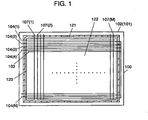
- Fig. 1 is a schematic plan view of a plasma display panel (PDP), with a front glass substrate removed, in accordance with an embodiment of the present invention.
- Fig. 2 is a perspective view of the PDP, showing an image display area in section.
- the number of display electrodes, display scan electrodes, and address electrodes is reduced for simplicity.
- PDP 100 includes front glass substrate 101 (not shown), rear glass substrate 102, N display electrodes 103, N display scan electrodes 104 (where a parenthesized N indicates the Nth electrode), M address electrode 107 (where a parenthesized M indicates the Mth electrode), and hermetic seal layer 121 shown by hatching.
- the PDP has an electrode matrix having a three-electrode structure made of display electrodes 103, display scan electrodes 104, and address electrodes 107. Display cells are formed at the respective intersections of display electrodes 103 and display scan electrodes 104, and address electrodes 107. Thus, image display area 123 is formed.
- This PDP 100 has, as shown in Fig. 2 , front glass substrate 101, and rear glass substrate 102 sealed to each other.
- the two substrates form discharge space 122 therebetween, which is filled with a discharge gas.
- display electrodes 103, display scan electrodes 104, dielectric glass layer 105, and MgO protective layer 106 are disposed on a principle surface of front glass substrate 101.
- display electrodes 103, display scan electrodes 104, dielectric glass layer 105, and MgO protective layer 106 are disposed on a principle surface of rear glass substrate 102.
- address electrodes 107, dielectric glass layer 108, barrier ribs 109, and phosphor layers 110R, 110G, and 110B are disposed on a principle surface of rear glass substrate 102.
- Such structured PDP is connected to a PDP driver 150 shown in Fig. 3 to form plasma display device 160.
- plasma display device 160 has display driver circuit 153, display scan driver circuit 154, and address driver circuit 155 in PDP 100.
- controller 152 a voltage is applied across display scan electrode 104 and address electrode 107 of a cell to be lit for address discharge therebetween.
- a pulse voltage is applied across display electrode 103 and display scan electrode 104, for sustain discharge.
- the sustain discharge generates ultraviolet light in the cell.
- the phosphor layers excited by the ultraviolet light emit light, thereby lighting the cell. In this way, combination of lit and unlit cells of the respective colors produces an image on the display.
- Fig. 4 is a sectional view illustrating the structure of an image display area of the PDP.
- N display electrodes 103 and N display scan electrodes 104 are arranged on front glass substrate 101 alternately, parallel to each other, like stripes. (In Fig. 2 , only two of respective electrodes are shown for simplicity.) Thereafter, the electrodes are covered with dielectric glass layer 105, and further over which, MgO protective layer 106 is formed.
- Display electrodes 103 and display scan electrodes 104 are formed of transparent electrodes made of indium thin oxide (ITO) and bus electrodes made of silver.
- the bus electrodes are formed by applying a silver paste by screen printing and then baking the paste.
- Dielectric glass layer 105 is formed by applying a paste containing lead glass material by screen printing, and baking the paste at a specified temperature for a specified period of time (e.g. at 560 °C for 20 min.) to obtain a desired thickness (approx. 20 ⁇ m).
- a paste containing lead glass material a mixture of PbO (70 wt%), B 2 O 3 (15 wt%), SiO 2 (10 wt%), Al 2 O 3 (5 wt%) and an organic binder ( ⁇ -terpineol containing 10% of ethyl cellulose dissolved therein) is used.
- the aforementioned organic binder contains a resin dissolved in an organic solvent.
- Acrylic resin can be used as a resin other than the ethyl cellulose, and n-butylcarbitol as an organic solvent. Further, a dispersant, e.g. glyceryl trileate, can be mixed into such an organic binder.
- a dispersant e.g. glyceryl trileate
- MgO protective layer 106 is made of magnesium oxide (MgO).
- the layer is formed into a specified thickness (approx. 0.5 ⁇ m) by sputtering or chemical vapor deposition (CVD) method.
- M address electrodes 107 are formed in lines on rear glass substrate 102 by screen-printing a silver paste for electrodes or a photolithography method and then baking the paste.
- dielectric glass layer 108 is formed by applying a paste containing lead glass material to the address electrodes by screen printing.
- barrier ribs 109 are formed by repeatedly applying the same paste containing lead glass material to the dielectric glass layer at a specified pitch by screen printing or by a photolithography method. These barrier ribs 109 divide, in the direction of the lines, discharge space 122 into respective cells (i.e. unit emission area).
- interval dimension W between barrier ribs 109 is determined to a value ranging from approx. 130 to 240 ⁇ m, according to a high definition television (HD-TV) screen having a diagonal size ranging from 32 to 50 in.
- HD-TV high definition television
- Red (R) phosphor particles are made of an yttrium oxide compound positively charged on their surfaces.
- Blue (B) phosphor particles are made of an aluminate compound having a ⁇ -alumina structure and positively charged on their surfaces.
- Green (G) phosphor particles are made of an aluminate compound having a ⁇ -alumina structure or an yttrium oxide compound positively charged on their surfaces.
- Paste-like phosphor ink made of red (R), green (G), or blue (B) phosphor particles and an organic binder is applied to grooves between barrier ribs 109, and baked at temperatures ranging from 400 to 590 °C to burn out the organic binder.
- phosphor layers 110R, 110B, and 110G - in which phosphor particles of corresponding colors are bound with each other - are formed. It is preferable that thickness L in the direction of lamination of phosphor layers 110R, 110B, and 110G on address electrodes 107 is approx. 8 to 25 times the average diameter of phosphor particles of each color That is, in order to constantly achieve a certain luminance (emission efficiency) when a phosphor layer is irradiated with an amount of ultraviolet light, the phosphor layer needs to absorb ultraviolet light generated in the discharged space, not allowing to pass therethrough. For this purpose, it is desirable that the phosphor layer has a thickness formed of at least eight layered-, preferably, approx.
- Phosphor particles having sufficiently small diameters and spherical shapes like those obtained by the hydrothermal synthesis method or the like, have a packing factor of the phosphor layer and a total surface area of the phosphor particles larger than those of phosphor particles having non-spherical shapes, even when the number of laminated layers are the same. As a result, phosphor particles having spherical shapes increase the surface area contributing to actual light emission of the phosphor layer, thereby enhancing the emission efficiency.
- the methods of synthesizing phosphor layers 110R, 11G, and 11B will be described later.
- the front panel and the rear panel produced in this manner are placed one on the other so that the respective electrodes on the front panel (display electrodes 103 and display scan electrodes 104) are orthogonal to the address electrodes 107 on the rear panel.
- Sealing glass is disposed between the panels along the periphery thereof and baked, for example, at temperatures of approx. 450 °C for 10 to 20 min. to form hermetical seal layer 121 (see Fig. 1 ) for sealing.
- discharge space 122 is once evacuated to a high vacuum (e.g. 1.1 ⁇ 10 -4 Pa) and filled with a discharge gas (e.g. He-Xe and Ne-Xe inert gas), at a specified pressure, to complete PDP 100.
- This PDP 100 is aged at a discharge voltage of 175V and at a frequency of 200 kHz: for five hours.
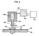
- Fig. 5 is a schematic diagram showing the structure of an ink dispenser used in forming phosphor layers.
- ink dispenser 200 includes server 210, pressure pump 220, and header 230.
- Phosphor ink is pressurized by pressure pump 220 and supplied from server 210, which stores the phosphor ink, to header 230.
- Header 230 includes ink chamber 230a and nozzle 240 (of which inner diameter ranges from 30 to 120 ⁇ m).
- the phosphor ink which has been fed to ink chamber 230a with application of pressure, is continuously ejected from nozzle 240.
- bore diameter D of nozzle 240 is sized at least 30 ⁇ m to prevent clogging of the nozzle.
- bore diameter D is equal to or smaller than interval W between barrier ribs 109 (approx. 130 to 200 ⁇ m) to properly apply the ink to the groove between the barrier ribs.
- bore diameter D is usually determined to 30 to 130 ⁇ m.
- Header 230 is structured to be driven lineally by a header scanning mechanism (not shown). Continuously ejecting phosphor ink 250 from nozzle 240 while scanning header 230 allow the phosphor ink to be uniformly applied to the grooves between barrier ribs 109 on rear glass substrate 102. Viscosity of the phosphor ink is kept within the range of 1,500 to 50,000 centipoises (CP) at a temperature of 25 °C.
- CP centipoises
- This server 210 also has a mixer (not shown). Mixing prevents precipitation of particles in the phosphor ink.
- Header 230 is integrally formed with ink chamber 230a and nozzle 240 by performing machining and electric discharge machining on a metallic material, inorganic material, or the like.
- Forming phosphor layers is not limited to the aforementioned method; other various kinds of methods, such as photolithography, screen printing, and a method of disposing a film including phosphor particles mixed therein, can be employed.
- the phosphor ink is prepared by mixing phosphor particles of each color, a binder, and a solvent so that the mixture has a viscosity ranging from 1,500 to 50,000 centipoises (CP).
- a surface active agent, silica, a dispersant (in amount of 0.1 to 5 wt%) can also be added, as required.
- red phosphor included in this phosphor ink a compound expressed by (Y, Gd) 1-x Eu x BO 3 or (Y 1-x Eu x ) 2 O 3 is used.
- the element Eu substitutes for a part of the element Y constituting the matrix of the compounds.
- the substitution value X of the element Eu with respect to the element Y is in the range of 0.01 ⁇ X ⁇ 0.3. Having X larger than 0.3 causes serious luminance degradation, although it achieves a high luminance. For this reason, such a red phosphor is unlikely to be practical.
- having X smaller than 0.01 lowers the composition ratio of Eu mainly emitting light, thus decreasing the luminance. The phosphor with decreased luminance can no longer serve as a phosphor.
- a compound expressed by xBaO ⁇ yMgO ⁇ zAl 2 O 3 ⁇ aMnO, xBaO ⁇ yAl 2 O 3 ⁇ zMnO, or YBO 3 :Tb and positively charged on its surface is used.
- Ba 1-x MgAl 10 O 17 :Eu x or Bal 1-x-y SryMgAl 10 O 17 :Eu x is used.
- Ba 1-x MgAl 10 O 17 :Eu x and Ba 1-x-y SryMgAl 10 O 17 :Eu x are compounds in which the element Eu or Eu and Sr substitute for a part of the element Ba constituting the matrix of the compounds.
- substitution values X, and Y of the element Eu and Sr with respect to the element Ba in the blue phosphor Ba 1-x-y SryMgAl 10 O 17 :Eu x should preferably be 0.03 ⁇ X ⁇ 0.2, and 0.1 ⁇ y ⁇ 0.5.
- Ethyl cellulose or acrylic resin can be used as a binder included in phosphor ink (in an amount of 0.1 to 10 wt% of the ink).
- ⁇ -terpineol or butylcarbitol can be used as a solvent.
- Polymers, such as PMA and PVA, can also be used as a binder.
- organic solvent, such as diethyleneglycol and methyl ether, can also be used.
- phosphor particles are fabricated by a solid-phase firing method, aqueous solution reaction method, atomization firing method, and hydrothermal synthesis method.
- aqueous solution reaction method atomization firing method
- hydrothermal synthesis method atomization firing method
- Ion-exchange water or pure water is preferably used for the aqueous medium in that it contains no impurities; however, an aqueous medium containing non-aqueous solvent (e.g. methanol and ethanol) can also be used.
- an aqueous medium containing non-aqueous solvent e.g. methanol and ethanol
- the hydrate mixed solution is put into a container made of a corrosion- and heat-resistant material, such as gold and platinum.
- the hydrate is hydro-thermally synthesized in a high pressure vessel, using equipment capable of heating and pressurizing at the same time, such as an autoclave, at specified temperatures (100 to 300°C) under specified pressures (0.2 to 10 MPa) for 12 to 20 hours.
- the obtained powder is baked in a reducing atmosphere (e.g. containing 5% of hydrogen and 95% of nitrogen), at a specified temperature for a specified period of time (e.g. at 1,350°C for two hours). Thereafter, the baked powder is classified to provide a desired blue phosphor, Ba 1-x MgAl 10 O 17 :Eu x . Then, the classified power is baked in an O 2 -N 2 atmosphere at temperatures ranging from 700 to 1,000°C to reduce the sites adsorbing water (H 2 O) or hydrocarbon (CxHy).
- a reducing atmosphere e.g. containing 5% of hydrogen and 95% of nitrogen
- a specified temperature for a specified period of time e.g. at 1,350°C for two hours.
- the baked powder is classified to provide a desired blue phosphor, Ba 1-x MgAl 10 O 17 :Eu x .
- the classified power is baked in an O 2 -N 2 atmosphere at temperatures ranging from 700 to 1,000°C to reduce
- trivalent Eu ions substitute for a part of bivalent ions (most of the Eu ions in a blue phosphor fabricated in a reducing atmosphere being bivalent) to fill oxygen vacancy.
- the blue phosphor can be fabricated by an atomizing method - atomizing the hydrate from a nozzle into a high-temperature furnace, without putting it in a gold or platinum container.
- the phosphor is different from the aforementioned Ba 1-x MgAl 10 O 17 :Eu x in the materials, and fabricated by a solid-phase reaction method. The materials thereof are described hereinafter.
- the materials i.e., barium hydroxide [Ba(OH) 2 ], strontium hydroxide [Sr(OH) 2 ], magnesium hydroxide [Mg(OH) 2 ], aluminum hydroxide [Al(OH) 3 ], and europium hydroxide [Eu(OH) 2 ] are weighted so as to have a required molar ratio.
- the materials are mixed with AlF 3 as a fluxing agent, and baked at specified temperatures (1,300 to 1,400°C) for a specified period of time (12 to 20 hours).
- Ba 1-x-y SryMgAl 10 O 17 :Eu x in which quadrivalent ions substitute for Mg and Al ions can be obtained.
- the average diameter of phosphor particles obtained by this method ranges from approx. 0.1 to 3.0 ⁇ m.
- a reducing atmosphere e.g. 5%H 2 -95%N 2
- specified temperatures 1,000 to 1,600°C
- specified period of time two hours
- the particles are classified by an air classifier to provide the phosphor particles.
- the particles are baked in an O 2 -N 2 atmosphere at temperatures ranging from 700 to 1,000°C.
- trivalent ions substitute for a part of bivalent Eu ions to fill oxygen vacancy.
- oxides, nitrides, and hydroxides are mainly used as the materials of the phosphors.
- the phosphors can be fabricated using organometallic compounds containing the elements Ba, Sr, Mg, Al, Eu, or the like, such as metal alkoxide and acetylacetone.
- the materials i.e., barium carbonate [BaCO 3 ], magnesium carbonate [MgCO 3 ], aluminum carbonate [Al 2 CO 3 ], manganese carbonate [MnCO 3 ] - light-emitting material, are prepared so as to have a required molar ratio.
- This compound is mixed with a small amount of fluxing agent (AlF 3 ), and baked in air at temperatures ranging from 1,200 to 1,500°C for two hours.
- AlF 3 fluxing agent
- the compound is lightly milled so that aggregate loosens, it is baked in a nitrogen atmosphere or an N 2 -H 2 atmosphere at temperatures ranging from 1,200 to 1,500°C, and milled again.
- the particles are baked in an oxygen atmosphere or an O 2 -N 2 atmosphere at temperatures ranging from 600 to 1,000°C.
- trivalent ions substitute for a part of bivalent Mn ions to fill oxygen vacancy, and a positively charged green phosphor is fabricated.
- the materials i.e. barium nitrate [Ba(NO 3 ) 2 ], lanthanoids nitrate [M(NO 3 ) 3 ], magnesium nitrate [Mg(NO 3 ) 2 ] and aluminum nitrate [Al(NO 3 ) 3 ⁇ 9H 2 O] are prepared in an aqueous solution so as to have a required a molar ratio.
- a required amount of manganese nitrate [Mn(NO 3 ) 2 ] and europium nitrate [Eu(NO 3 ) 3 ⁇ 9H 2 O] are added, to fabricate a mixed solution.
- an aqueous base e.g. ammonia aqueous solution
- this hydrate and ion-exchange water are put into a container made of a corrosion- and heat-resistant material, such as platinum and gold.
- This mixed solution is hydro-thermally synthesized in a high-pressure vessel, using an autoclave, for example, at specified temperatures under specified pressures for specified periods of time (e.g. 100 to 300°C, 0.2 to 10 MPa, 2 to 20 hours). Then the solution is dried to provide a phosphor xBaO ⁇ yMgO ⁇ zAl 2 O 3 ⁇ aMnO.
- this powder is baked in a N 2 atmosphere or a N 2 -H 2 atmosphere at temperatures ranging from 1, 200 to 1,500°C, to fabricate a positively charged green phosphor.
- the particle diameter grows to 5 to 15 ⁇ m.
- these particles are milled by a jet mill until the average diameter reaches 0.1 to 3 ⁇ m, they are baked in air or a N 2 -O 2 atmosphere at temperatures ranging from 600 to 1,000°C, to reduce the sites adsorbing water (H 2 O) or hydrocarbon (CxHy).
- H 2 O adsorbing water
- CxHy hydrocarbon
- the materials i.e. Y 2 O 3 , B 2 O 3 , and TB 2 O 3 , are prepared so as to have a required molar ratio of the phosphor.
- the materials are mixed with a small amount of fluxing agent (NH 4 Cl), baked in a N 2 atmosphere or in a N 2 -H 2 atmosphere at temperatures ranging from 1,000 to 1,400°C, and then baked in a N 2 -O 2 atmosphere at temperatures ranging from 600 to 900°C.
- a positively charged green phosphor without oxygen vacancy can be provided.
- This mixture is heat-treated in air at temperatures ranging from 1,200 to 1,350°C for two hours and classified, to provide a red phosphor. Because the red phosphor is baked in air, oxygen vacancy is relatively small even if the mixture is not baked in an O 2 -N 2 atmosphere. However, defects may occur in the classifying process; thus baking in an O 2 -N 2 atmosphere is preferable.
- the mixture is dissolved in ion-exchange water, to fabricate a mixed solution.
- an aqueous base e.g. ammonia aqueous solution
- is added to the mixed solution to provide a hydrate.
- the hydrate and ion-exchange water are put into a container made of a corrosion- and heat-resistant material, such as gold and platinum. Then, the container holding the mixed solution is put into a high-pressure vessel to undergo hydrothermal synthesis.
- the hydrothermal synthesis takes place for 3 to 12 hours at temperatures ranging from 100 to 300 °C under pressures ranging from 0.2 to 10 MPa, using an autoclave, for example.
- the compound obtained by hydrothermal synthesis is dried, to provide a desired phosphor of Y 2-x O 3 :Eu x .
- the phosphor is baked in air at temperatures ranging from 1,300 to 1,400 °C for two hours and then classified.
- the red phosphor is thus obtained.
- the phosphor obtained by the hydrothermal synthesis process has a spherical shape and particle diameters ranging from approx. 0.1 to 2.0 ⁇ m. Such a diameter and shape are suitable for forming a phosphor layer that exhibits excellent light emission characteristics. Because these red phosphors are baked in air, oxygen vacancy is smaller and thus adsorption of water (H 2 O) or hydrocarbon (CxHy) is smaller.
- each of the plasma display devices produced has a diagonal size of 42 in. - for a high definition (HD) TV screen having a rib-pitch of 150 ⁇ m.
- Each of the PDPs was produced so that the dielectric glass layer was 20 ⁇ m thick; the MgO protective layer was 0.5 ⁇ m thick; and the distance between the display electrode and the display scan electrode was 0.08 mm.
- the discharge space was filled with a discharge gas in which 5% of xenon gas was mixed into neon as the major component.
- the discharge gas was filled in the discharge space with the application of a pressure of 66.5 kPa.
- Each of sample Nos. 1 through 6 shows evaluation results of a plasma display device using a green phosphor xBaO ⁇ yMgO ⁇ zAl 2 O 3 ⁇ aMnO, which is fabricated by baking in an O 2 -N 2 atmosphere and positively charged, and a red phosphor (Y, Gd) 1-x BO 3 :Eu x , and a blue phosphor BaO 1-x MgAl 10 O 17 :Eu x .
- the methods of synthesizing the phosphors, the composition x, y, z, and a of respective materials, and the amounts of trivalent ions with respect to bivalent Eu ions are changed as shown in Table 1.
- Each of sample Nos. 7 through11 shows evaluation results of a plasma display device using a green phosphor xBaO ⁇ yAl 2 O 3 ⁇ zMnO, which is fabricated by baking in an O 2 -N 2 atmosphere, and a red phosphor Y 1-x O 3 :Eu x , and a blue phosphor Ba 1-x-y Sr y MgAl 10 O 17 :Eu x .
- the methods of synthesizing the phosphors, the composition x, y, and z, of respective materials, and the amounts of trivalent ions with respect to bivalent Mn and Eu ions are changed as shown in Table 1.
- Each of sample Nos. 12 through 16 is a panel using a mixture of xBaO ⁇ yAl 2 O 3 ⁇ zMnO and ReBO 3 :Tb - both fabricated by baking in an O 2 -N 2 atmosphere and positively charged, as a green phosphor, and a red phosphor (Y 1-x ) 2 O 3 :Eu x , and a blue phosphor Ba 1-x Eu x MgAl 10 O 17 .
- the methods of synthesizing the phosphors, the composition x, y, and z of respective materials, and the amounts of trivalent ions with respect to bivalent Mn and Eu ions are changed as shown in Table 1.
- Sample No. 6 is a comparative sample, a panel using a blue phosphor that is not sufficiently baked in an O 2 -N 2 atmosphere (the amount of trivalent Eu ions being 1%). Phosphors of other colors are the same as those of sample No. 5.
- Sample No. 11 is also a comparative sample, a panel using a green phosphor that is not sufficiently baked in an O 2 -N 2 atmosphere (the amount of trivalent Mn ions being 0.1%). Phosphors of other colors are the same as those of sample No. 10.
- Sample No. 17 is also a comparative sample that has 50% of Zn 2 SiO 4 :Mn mixed in the green phosphor. The red phosphor and blue phosphor are the same as those of sample No. 12.
- Sample No. 18 is also a comparative sample, a panel using a green phosphor Zn 2 SiO 4 :Mn negatively charged, and a conventional blue phosphor Ba 1-x Eu x MgAl 10 O 17 containing less trivalent Eu
- Phosphor ink used for forming phosphor layers was prepared by using each kind of phosphor particles shown in Table 1, and mixing the phosphor, resin, solvent and dispersant. According to the measurement results, viscosity of each kind of the phosphor ink (at 25°C) is kept within the range of 1,500 to 50,000 centipoises (CP). Observations on each phosphor layer formed showed that the phosphor ink was uniformly applied to the side faces of the barrier ribs. In production of each sample, the bore diameter of the nozzle used for application is 100 ⁇ m.
- the phosphor particles used for the phosphor layers have an average diameter ranging from 0.1 to 3.0 ⁇ m and a maximum diameter up to 8 ⁇ m.
- the phosphors (blue, green, and red) in the produced PDPs were taken out, and the amount of adsorbed water (H 2 O), carbon monoxide (CO), and carbon dioxide (CO 2 ) was measured by a thermal desorption spectroscopy (TDS).
- TDS thermal desorption spectroscopy
- the luminance (white, green, blue, and red) and color temperature of each PDP after the PDP manufacturing process were measured with a luminance meter.
- luminance degradation and color temperature were measured as follows. Discharge sustain pulses at a voltage of 175V and at a frequency of 200 kHz were applied to each plasma display device continuously for 500 hours, and the luminance and color temperature of each PDP were measured before and after the application of the pulses. From the measurements, a luminance degradation factor ([luminance after application luminance before application]/luminance before application)*100) and a color temperature change factor were determined.
- the ratio of bivalent and trivalent Mn and Eu ions was measured by an X-ray absorption near edge structure (XANES) spectrum method.
- the combination of phosphors used for the PDPs include a green phosphor xBaO ⁇ yAl 2 O 3 ⁇ zMnO and BaO ⁇ yMgO ⁇ zAl 2 O 3 ⁇ aMnO, and a blue phosphor Ba 1-x Eu x MgAl 10 O 17 . Because these phosphors are not baked in an O 2 -N 2 atmosphere, they are likely to adsorb water (H 2 O) or hydrocarbon (CxHy).
- adsorption of water is three to seven times as much as that of the phosphor that has been baked.
- the absolute amount of the adsorbed water is one fifth to one tenth the amount of water; however, the amount of adsorbed carbon monoxide (CO), carbon dioxide (CO 2 ), and hydrocarbon (CxHy) is large.
- This adsorption causes significant luminance degradation of green and blue during discharge (driving) and significant decrease in the luminance and color temperature (color shift) at white display on the entire panel.
- nozzle clogging does not occur.
- each of these PDPs use a positively charged green phosphor xBaO ⁇ yMgO ⁇ zAl 2 O 3 ⁇ aMnO or xBaO ⁇ yAl 2 O 3 ⁇ zMnO having a ⁇ -alumina single crystal structure, and a blue phosphor Ba 1-x Eu x MgAl 10 O 17 or Ba 1-x-y Eu x Sr y MgAl 10 O 17 , both of which are baked in an O 2 atmosphere or an O 2 -N 2 atmosphere.
- the present invention can stabilize the application of phosphor layers and provide a highly reliable plasma display device having no decrease in the luminance and color temperature and no addressing failure of the panel.
- a plasma display device of the present invention can realize a highly reliable plasma display device having no decrease in the luminance and color temperature and no addressing failure of the panel.
- This plasma display device is useful as an image display device or the like for a TV set or the like.
Landscapes
- Chemical & Material Sciences (AREA)
- Engineering & Computer Science (AREA)
- Inorganic Chemistry (AREA)
- Materials Engineering (AREA)
- Organic Chemistry (AREA)
- Physics & Mathematics (AREA)
- Plasma & Fusion (AREA)
- Luminescent Compositions (AREA)
- Gas-Filled Discharge Tubes (AREA)
Abstract
Claims (5)
- Dispositif d'affichage à plasma comprenant un panneau d'affichage à plasma dans lequel une pluralité de cellules de décharge ayant une pluralité de couleurs sont disposées, des couches luminophores ayant une couleur qui correspond aux cellules de décharge respectives sont disposées, et les couches luminophores sont excitées par une lumière ultraviolette pour émettre de la lumière, dans lequel les couches luminophores comprennent:une couche luminophore verte (110G) réalisée en l'un parmi un luminophore composé d'aluminate ayant une structure cristalline β-alumine sélectionné parmi un composé exprimé par xBaO·yMgO·zAl2O3·aMnO (où, 0, 7 ≤ x ≤ 0,95, 0,05 ≤ y ≤ 0,2, 5,0 ≤ z ≤ 6.0, et 0,05 ≤ a ≤ 0,2) et un composé exprimé par xBaO·yAl2O3·zMnO (où, 0,7 ≤ x ≤ 0,95, 5 ≤ y ≤ 6, et 0,05 ≤ z ≤ 0,2), dans lequel des ions trivalents se substituent à une partie d'ions bivalents de Mn, ou réalisée en l'un dudit luminophore composé d'aluminate ayant une structure cristalline β-alumine mélangé avec un composé d'oxyde exprimé par ReBO3:Tb (où Re est l'un de Y, Sc, La, Ce et Gd) ;une couche luminophore bleu (110B) réalisée en un luminophore composé d'aluminate ayant une structure cristalline β-alumine ; etune couche luminophore rouge (110R) réalisée en un luminophore composé d'oxyde d'yttrium.
- Dispositif d'affichage à plasma selon la revendication 1, dans lequel des atomes de Mn dans le luminophore vert du composé d'aluminate ont une concentration en ions bivalents de Mn se trouvant dans la plage de 80 à 99% et une concentration en ions trivalents de Mn se trouvant dans la plage de 1 à 20%.
- Dispositif d'affichage à plasma selon la revendication 1, dans lequel le luminophore bleu réalisé en composé d'aluminate est un composé exprimé par l'un parmi Ba1-xEuxMgAl10O17 et Ba1-x-yEuxSryMgAl10O17 (où 0,05 ≤ x ≤ 0,2, et 0,05 ≤ y ≤ 0,5).
- Dispositif d'affichage à plasma de la revendication 3, dans lequel des atomes d'Eu dans le luminophore bleu ont une concentration en ions bivalents d'Eu se trouvant dans la plage de 40 à 90% et une concentration en ions trivalents d'Eu se trouvant dans la plage de 10 à 60%.
- Dispositif d'affichage à plasma de la revendication 1, dans lequel le luminophore rouge est un composé exprimé par l'un parmi (Y, Gd)1-xEuxB03 et (Y1-xEux) 2O3 (où, 0,01 ≤ x ≤ 0, 3) .
Applications Claiming Priority (5)
| Application Number | Priority Date | Filing Date | Title |
|---|---|---|---|
| JP2002283185 | 2002-09-27 | ||
| JP2002283185 | 2002-09-27 | ||
| JP2002313911 | 2002-10-29 | ||
| JP2002313911 | 2002-10-29 | ||
| PCT/JP2003/012347 WO2004030009A1 (fr) | 2002-09-27 | 2003-09-26 | Ecran a plasma |
Publications (3)
| Publication Number | Publication Date |
|---|---|
| EP1480247A1 EP1480247A1 (fr) | 2004-11-24 |
| EP1480247A4 EP1480247A4 (fr) | 2010-09-29 |
| EP1480247B1 true EP1480247B1 (fr) | 2011-08-24 |
Family
ID=32044634
Family Applications (1)
| Application Number | Title | Priority Date | Filing Date |
|---|---|---|---|
| EP03798526A Expired - Lifetime EP1480247B1 (fr) | 2002-09-27 | 2003-09-26 | Ecran a plasma |
Country Status (5)
| Country | Link |
|---|---|
| US (1) | US7531961B2 (fr) |
| EP (1) | EP1480247B1 (fr) |
| KR (1) | KR100621125B1 (fr) |
| CN (1) | CN100590773C (fr) |
| WO (1) | WO2004030009A1 (fr) |
Families Citing this family (6)
| Publication number | Priority date | Publication date | Assignee | Title |
|---|---|---|---|---|
| FR2864694A1 (fr) * | 2004-07-01 | 2005-07-01 | Thomson Plasma | Panneau a plasma a luminophores de charges statiques homogenes |
| KR20070005392A (ko) * | 2005-07-06 | 2007-01-10 | 삼성에스디아이 주식회사 | 형광막 형성용 조성물과 이로부터 제조된 표시장치 및 이의제조방법 |
| JP4645463B2 (ja) * | 2006-01-27 | 2011-03-09 | 船井電機株式会社 | テレビジョン放送受信記録装置 |
| JP5121167B2 (ja) * | 2006-05-19 | 2013-01-16 | キヤノン株式会社 | 青色蛍光体及びその用途 |
| KR100932984B1 (ko) | 2008-02-01 | 2009-12-21 | 삼성에스디아이 주식회사 | 디스플레이 장치용 적색 형광체 및 이를 포함하는디스플레이 장치 |
| CN107488450A (zh) | 2016-06-09 | 2017-12-19 | 日亚化学工业株式会社 | 铝酸盐荧光体、发光装置及铝酸盐荧光体的制造方法 |
Family Cites Families (7)
| Publication number | Priority date | Publication date | Assignee | Title |
|---|---|---|---|---|
| JPS59226087A (ja) * | 1983-06-07 | 1984-12-19 | Toshiba Corp | 螢光ランプ |
| JP3587661B2 (ja) * | 1997-09-12 | 2004-11-10 | 富士通株式会社 | プラズマディスプレイパネル |
| JP3045229B2 (ja) | 1997-10-14 | 2000-05-29 | 日本電気株式会社 | プラズマディスプレイパネル |
| JPH11140437A (ja) | 1997-11-06 | 1999-05-25 | Matsushita Electric Ind Co Ltd | 二価ユーロピウム付活蛍光体の製造方法 |
| JP2000251701A (ja) | 1999-02-26 | 2000-09-14 | Toray Ind Inc | ディスプレイの製造方法 |
| TW533447B (en) * | 1999-12-14 | 2003-05-21 | Matsushita Electric Ind Co Ltd | Plasma display apparatus |
| JP2003336052A (ja) * | 2002-05-17 | 2003-11-28 | Matsushita Electric Ind Co Ltd | プラズマディスプレイ装置 |
-
2003
- 2003-09-26 KR KR1020047013593A patent/KR100621125B1/ko not_active IP Right Cessation
- 2003-09-26 WO PCT/JP2003/012347 patent/WO2004030009A1/fr active Application Filing
- 2003-09-26 CN CN03804990A patent/CN100590773C/zh not_active Expired - Fee Related
- 2003-09-26 EP EP03798526A patent/EP1480247B1/fr not_active Expired - Lifetime
- 2003-09-26 US US10/503,301 patent/US7531961B2/en not_active Expired - Fee Related
Also Published As
| Publication number | Publication date |
|---|---|
| CN1639825A (zh) | 2005-07-13 |
| US7531961B2 (en) | 2009-05-12 |
| EP1480247A1 (fr) | 2004-11-24 |
| KR20040086471A (ko) | 2004-10-08 |
| US20050146271A1 (en) | 2005-07-07 |
| WO2004030009A1 (fr) | 2004-04-08 |
| EP1480247A4 (fr) | 2010-09-29 |
| CN100590773C (zh) | 2010-02-17 |
| KR100621125B1 (ko) | 2006-09-13 |
Similar Documents
| Publication | Publication Date | Title |
|---|---|---|
| KR100572432B1 (ko) | 플라즈마 디스플레이 장치, 그에 사용되는 형광체 및 그의 제조 방법 | |
| US7208102B2 (en) | Plasma display unit, phosphor and process for producing phosphor | |
| EP1426430B1 (fr) | Ecran a plasma, materiau fluorescent et procede de fabrication du materiau fluorescent | |
| EP1350829B1 (fr) | Matiere fluorescente, son procede de fabrication et ecran a plasma | |
| EP1426431B1 (fr) | Ecran a plasma, materiau fluorescent et procede de fabrication du materiau fluorescent | |
| US7268492B2 (en) | Plasma display device with green emitting phosphor that becomes positively charged | |
| US7423376B2 (en) | Plasma display device | |
| US7576487B2 (en) | Plasma display device | |
| KR100572431B1 (ko) | 플라즈마 표시 장치, 형광체 및 형광체의 제조 방법 | |
| US7423368B2 (en) | Plasma display and method of producing phosphor used therein | |
| EP1480247B1 (fr) | Ecran a plasma | |
| JP3818285B2 (ja) | プラズマディスプレイ装置 | |
| JP4556908B2 (ja) | プラズマディスプレイ装置 | |
| JP2004091623A (ja) | プラズマディスプレイパネル | |
| JP2004067874A (ja) | プラズマディスプレイパネル |
Legal Events
| Date | Code | Title | Description |
|---|---|---|---|
| PUAI | Public reference made under article 153(3) epc to a published international application that has entered the european phase |
Free format text: ORIGINAL CODE: 0009012 |
|
| 17P | Request for examination filed |
Effective date: 20040806 |
|
| AK | Designated contracting states |
Kind code of ref document: A1 Designated state(s): AT BE BG CH CY CZ DE DK EE ES FI FR GB GR HU IE IT LI LU MC NL PT RO SE SI SK TR |
|
| AX | Request for extension of the european patent |
Extension state: AL LT LV MK |
|
| DAX | Request for extension of the european patent (deleted) | ||
| RBV | Designated contracting states (corrected) |
Designated state(s): DE FR GB NL |
|
| RAP1 | Party data changed (applicant data changed or rights of an application transferred) |
Owner name: PANASONIC CORPORATION |
|
| A4 | Supplementary search report drawn up and despatched |
Effective date: 20100831 |
|
| 17Q | First examination report despatched |
Effective date: 20101207 |
|
| GRAP | Despatch of communication of intention to grant a patent |
Free format text: ORIGINAL CODE: EPIDOSNIGR1 |
|
| RIC1 | Information provided on ipc code assigned before grant |
Ipc: C09K 11/78 20060101ALI20110330BHEP Ipc: C09K 11/64 20060101ALI20110330BHEP Ipc: H01J 11/02 20060101AFI20110330BHEP Ipc: C09K 11/08 20060101ALI20110330BHEP |
|
| GRAS | Grant fee paid |
Free format text: ORIGINAL CODE: EPIDOSNIGR3 |
|
| GRAA | (expected) grant |
Free format text: ORIGINAL CODE: 0009210 |
|
| AK | Designated contracting states |
Kind code of ref document: B1 Designated state(s): DE FR GB NL |
|
| REG | Reference to a national code |
Ref country code: GB Ref legal event code: FG4D |
|
| REG | Reference to a national code |
Ref country code: DE Ref legal event code: R096 Ref document number: 60338216 Country of ref document: DE Effective date: 20111027 |
|
| REG | Reference to a national code |
Ref country code: NL Ref legal event code: VDEP Effective date: 20110824 |
|
| PG25 | Lapsed in a contracting state [announced via postgrant information from national office to epo] |
Ref country code: NL Free format text: LAPSE BECAUSE OF FAILURE TO SUBMIT A TRANSLATION OF THE DESCRIPTION OR TO PAY THE FEE WITHIN THE PRESCRIBED TIME-LIMIT Effective date: 20110824 |
|
| PLBE | No opposition filed within time limit |
Free format text: ORIGINAL CODE: 0009261 |
|
| STAA | Information on the status of an ep patent application or granted ep patent |
Free format text: STATUS: NO OPPOSITION FILED WITHIN TIME LIMIT |
|
| 26N | No opposition filed |
Effective date: 20120525 |
|
| REG | Reference to a national code |
Ref country code: DE Ref legal event code: R097 Ref document number: 60338216 Country of ref document: DE Effective date: 20120525 |
|
| PGFP | Annual fee paid to national office [announced via postgrant information from national office to epo] |
Ref country code: GB Payment date: 20120926 Year of fee payment: 10 |
|
| PGFP | Annual fee paid to national office [announced via postgrant information from national office to epo] |
Ref country code: FR Payment date: 20120926 Year of fee payment: 10 Ref country code: DE Payment date: 20120919 Year of fee payment: 10 |
|
| REG | Reference to a national code |
Ref country code: DE Ref legal event code: R119 Ref document number: 60338216 Country of ref document: DE |
|
| GBPC | Gb: european patent ceased through non-payment of renewal fee |
Effective date: 20130926 |
|
| REG | Reference to a national code |
Ref country code: FR Ref legal event code: ST Effective date: 20140530 |
|
| PG25 | Lapsed in a contracting state [announced via postgrant information from national office to epo] |
Ref country code: GB Free format text: LAPSE BECAUSE OF NON-PAYMENT OF DUE FEES Effective date: 20130926 |
|
| PG25 | Lapsed in a contracting state [announced via postgrant information from national office to epo] |
Ref country code: DE Free format text: LAPSE BECAUSE OF NON-PAYMENT OF DUE FEES Effective date: 20140401 Ref country code: FR Free format text: LAPSE BECAUSE OF NON-PAYMENT OF DUE FEES Effective date: 20130930 |
|
| REG | Reference to a national code |
Ref country code: DE Ref legal event code: R079 Ref document number: 60338216 Country of ref document: DE Free format text: PREVIOUS MAIN CLASS: H01J0011020000 Ipc: H01J0011000000 |
|
| REG | Reference to a national code |
Ref country code: DE Ref legal event code: R119 Ref document number: 60338216 Country of ref document: DE Effective date: 20140401 Ref country code: DE Ref legal event code: R079 Ref document number: 60338216 Country of ref document: DE Free format text: PREVIOUS MAIN CLASS: H01J0011020000 Ipc: H01J0011000000 Effective date: 20141029 |