EP1478023A1 - Module part - Google Patents
Module part Download PDFInfo
- Publication number
- EP1478023A1 EP1478023A1 EP03705323A EP03705323A EP1478023A1 EP 1478023 A1 EP1478023 A1 EP 1478023A1 EP 03705323 A EP03705323 A EP 03705323A EP 03705323 A EP03705323 A EP 03705323A EP 1478023 A1 EP1478023 A1 EP 1478023A1
- Authority
- EP
- European Patent Office
- Prior art keywords
- circuit substrate
- module component
- junction
- recited
- junction circuit
- Prior art date
- Legal status (The legal status is an assumption and is not a legal conclusion. Google has not performed a legal analysis and makes no representation as to the accuracy of the status listed.)
- Withdrawn
Links
Images







Classifications
-
- H—ELECTRICITY
- H10—SEMICONDUCTOR DEVICES; ELECTRIC SOLID-STATE DEVICES NOT OTHERWISE PROVIDED FOR
- H10W—GENERIC PACKAGES, INTERCONNECTIONS, CONNECTORS OR OTHER CONSTRUCTIONAL DETAILS OF DEVICES COVERED BY CLASS H10
- H10W70/00—Package substrates; Interposers; Redistribution layers [RDL]
- H10W70/01—Manufacture or treatment
- H10W70/05—Manufacture or treatment of insulating or insulated package substrates, or of interposers, or of redistribution layers
-
- G—PHYSICS
- G01—MEASURING; TESTING
- G01R—MEASURING ELECTRIC VARIABLES; MEASURING MAGNETIC VARIABLES
- G01R31/00—Arrangements for testing electric properties; Arrangements for locating electric faults; Arrangements for electrical testing characterised by what is being tested not provided for elsewhere
- G01R31/28—Testing of electronic circuits, e.g. by signal tracer
-
- H—ELECTRICITY
- H05—ELECTRIC TECHNIQUES NOT OTHERWISE PROVIDED FOR
- H05K—PRINTED CIRCUITS; CASINGS OR CONSTRUCTIONAL DETAILS OF ELECTRIC APPARATUS; MANUFACTURE OF ASSEMBLAGES OF ELECTRICAL COMPONENTS
- H05K1/00—Printed circuits
- H05K1/18—Printed circuits structurally associated with non-printed electric components
- H05K1/182—Printed circuits structurally associated with non-printed electric components associated with components mounted in printed circuit boards [PCB], e.g. insert-mounted components [IMC]
- H05K1/185—Printed circuits structurally associated with non-printed electric components associated with components mounted in printed circuit boards [PCB], e.g. insert-mounted components [IMC] associated with components encapsulated in the insulating substrate of the PCBs; associated with components incorporated in internal layers of multilayer circuit boards
- H05K1/186—Printed circuits structurally associated with non-printed electric components associated with components mounted in printed circuit boards [PCB], e.g. insert-mounted components [IMC] associated with components encapsulated in the insulating substrate of the PCBs; associated with components incorporated in internal layers of multilayer circuit boards manufactured by mounting on or connecting to patterned circuits before or during embedding
-
- H—ELECTRICITY
- H10—SEMICONDUCTOR DEVICES; ELECTRIC SOLID-STATE DEVICES NOT OTHERWISE PROVIDED FOR
- H10W—GENERIC PACKAGES, INTERCONNECTIONS, CONNECTORS OR OTHER CONSTRUCTIONAL DETAILS OF DEVICES COVERED BY CLASS H10
- H10W70/00—Package substrates; Interposers; Redistribution layers [RDL]
- H10W70/60—Insulating or insulated package substrates; Interposers; Redistribution layers
- H10W70/611—Insulating or insulated package substrates; Interposers; Redistribution layers for connecting multiple chips together
-
- H—ELECTRICITY
- H10—SEMICONDUCTOR DEVICES; ELECTRIC SOLID-STATE DEVICES NOT OTHERWISE PROVIDED FOR
- H10W—GENERIC PACKAGES, INTERCONNECTIONS, CONNECTORS OR OTHER CONSTRUCTIONAL DETAILS OF DEVICES COVERED BY CLASS H10
- H10W70/00—Package substrates; Interposers; Redistribution layers [RDL]
- H10W70/60—Insulating or insulated package substrates; Interposers; Redistribution layers
- H10W70/611—Insulating or insulated package substrates; Interposers; Redistribution layers for connecting multiple chips together
- H10W70/614—Insulating or insulated package substrates; Interposers; Redistribution layers for connecting multiple chips together the multiple chips being integrally enclosed
-
- H—ELECTRICITY
- H10—SEMICONDUCTOR DEVICES; ELECTRIC SOLID-STATE DEVICES NOT OTHERWISE PROVIDED FOR
- H10W—GENERIC PACKAGES, INTERCONNECTIONS, CONNECTORS OR OTHER CONSTRUCTIONAL DETAILS OF DEVICES COVERED BY CLASS H10
- H10W70/00—Package substrates; Interposers; Redistribution layers [RDL]
- H10W70/60—Insulating or insulated package substrates; Interposers; Redistribution layers
- H10W70/67—Insulating or insulated package substrates; Interposers; Redistribution layers characterised by their insulating layers or insulating parts
- H10W70/68—Shapes or dispositions thereof
- H10W70/685—Shapes or dispositions thereof comprising multiple insulating layers
-
- H—ELECTRICITY
- H10—SEMICONDUCTOR DEVICES; ELECTRIC SOLID-STATE DEVICES NOT OTHERWISE PROVIDED FOR
- H10W—GENERIC PACKAGES, INTERCONNECTIONS, CONNECTORS OR OTHER CONSTRUCTIONAL DETAILS OF DEVICES COVERED BY CLASS H10
- H10W70/00—Package substrates; Interposers; Redistribution layers [RDL]
- H10W70/60—Insulating or insulated package substrates; Interposers; Redistribution layers
- H10W70/67—Insulating or insulated package substrates; Interposers; Redistribution layers characterised by their insulating layers or insulating parts
- H10W70/69—Insulating materials thereof
-
- H—ELECTRICITY
- H10—SEMICONDUCTOR DEVICES; ELECTRIC SOLID-STATE DEVICES NOT OTHERWISE PROVIDED FOR
- H10W—GENERIC PACKAGES, INTERCONNECTIONS, CONNECTORS OR OTHER CONSTRUCTIONAL DETAILS OF DEVICES COVERED BY CLASS H10
- H10W90/00—Package configurations
-
- H—ELECTRICITY
- H10—SEMICONDUCTOR DEVICES; ELECTRIC SOLID-STATE DEVICES NOT OTHERWISE PROVIDED FOR
- H10W—GENERIC PACKAGES, INTERCONNECTIONS, CONNECTORS OR OTHER CONSTRUCTIONAL DETAILS OF DEVICES COVERED BY CLASS H10
- H10W90/00—Package configurations
- H10W90/401—Package configurations characterised by multiple insulating or insulated package substrates, interposers or RDLs
-
- H—ELECTRICITY
- H05—ELECTRIC TECHNIQUES NOT OTHERWISE PROVIDED FOR
- H05K—PRINTED CIRCUITS; CASINGS OR CONSTRUCTIONAL DETAILS OF ELECTRIC APPARATUS; MANUFACTURE OF ASSEMBLAGES OF ELECTRICAL COMPONENTS
- H05K1/00—Printed circuits
- H05K1/16—Printed circuits incorporating printed electric components, e.g. printed resistors, capacitors or inductors
-
- H—ELECTRICITY
- H05—ELECTRIC TECHNIQUES NOT OTHERWISE PROVIDED FOR
- H05K—PRINTED CIRCUITS; CASINGS OR CONSTRUCTIONAL DETAILS OF ELECTRIC APPARATUS; MANUFACTURE OF ASSEMBLAGES OF ELECTRICAL COMPONENTS
- H05K2201/00—Indexing scheme relating to printed circuits covered by H05K1/00
- H05K2201/07—Electric details
- H05K2201/0707—Shielding
- H05K2201/0723—Shielding provided by an inner layer of PCB
-
- H—ELECTRICITY
- H05—ELECTRIC TECHNIQUES NOT OTHERWISE PROVIDED FOR
- H05K—PRINTED CIRCUITS; CASINGS OR CONSTRUCTIONAL DETAILS OF ELECTRIC APPARATUS; MANUFACTURE OF ASSEMBLAGES OF ELECTRICAL COMPONENTS
- H05K2203/00—Indexing scheme relating to apparatus or processes for manufacturing printed circuits covered by H05K3/00
- H05K2203/06—Lamination
- H05K2203/063—Lamination of preperforated insulating layer
-
- H—ELECTRICITY
- H05—ELECTRIC TECHNIQUES NOT OTHERWISE PROVIDED FOR
- H05K—PRINTED CIRCUITS; CASINGS OR CONSTRUCTIONAL DETAILS OF ELECTRIC APPARATUS; MANUFACTURE OF ASSEMBLAGES OF ELECTRICAL COMPONENTS
- H05K2203/00—Indexing scheme relating to apparatus or processes for manufacturing printed circuits covered by H05K3/00
- H05K2203/11—Treatments characterised by their effect, e.g. heating, cooling, roughening
- H05K2203/1147—Sealing or impregnating, e.g. of pores
-
- H—ELECTRICITY
- H05—ELECTRIC TECHNIQUES NOT OTHERWISE PROVIDED FOR
- H05K—PRINTED CIRCUITS; CASINGS OR CONSTRUCTIONAL DETAILS OF ELECTRIC APPARATUS; MANUFACTURE OF ASSEMBLAGES OF ELECTRICAL COMPONENTS
- H05K2203/00—Indexing scheme relating to apparatus or processes for manufacturing printed circuits covered by H05K3/00
- H05K2203/16—Inspection; Monitoring; Aligning
- H05K2203/167—Using mechanical means for positioning, alignment or registration, e.g. using rod-in-hole alignment
-
- H—ELECTRICITY
- H05—ELECTRIC TECHNIQUES NOT OTHERWISE PROVIDED FOR
- H05K—PRINTED CIRCUITS; CASINGS OR CONSTRUCTIONAL DETAILS OF ELECTRIC APPARATUS; MANUFACTURE OF ASSEMBLAGES OF ELECTRICAL COMPONENTS
- H05K2203/00—Indexing scheme relating to apparatus or processes for manufacturing printed circuits covered by H05K3/00
- H05K2203/17—Post-manufacturing processes
- H05K2203/171—Tuning, e.g. by trimming of printed components or high frequency circuits
-
- H—ELECTRICITY
- H05—ELECTRIC TECHNIQUES NOT OTHERWISE PROVIDED FOR
- H05K—PRINTED CIRCUITS; CASINGS OR CONSTRUCTIONAL DETAILS OF ELECTRIC APPARATUS; MANUFACTURE OF ASSEMBLAGES OF ELECTRICAL COMPONENTS
- H05K3/00—Apparatus or processes for manufacturing printed circuits
- H05K3/10—Apparatus or processes for manufacturing printed circuits in which conductive material is applied to the insulating support in such a manner as to form the desired conductive pattern
- H05K3/20—Apparatus or processes for manufacturing printed circuits in which conductive material is applied to the insulating support in such a manner as to form the desired conductive pattern by affixing prefabricated conductor pattern
-
- H—ELECTRICITY
- H05—ELECTRIC TECHNIQUES NOT OTHERWISE PROVIDED FOR
- H05K—PRINTED CIRCUITS; CASINGS OR CONSTRUCTIONAL DETAILS OF ELECTRIC APPARATUS; MANUFACTURE OF ASSEMBLAGES OF ELECTRICAL COMPONENTS
- H05K3/00—Apparatus or processes for manufacturing printed circuits
- H05K3/40—Forming printed elements for providing electric connections to or between printed circuits
- H05K3/4038—Through-connections; Vertical interconnect access [VIA] connections
- H05K3/4053—Through-connections; Vertical interconnect access [VIA] connections by thick-film techniques
- H05K3/4069—Through-connections; Vertical interconnect access [VIA] connections by thick-film techniques for via connections in organic insulating substrates
-
- H—ELECTRICITY
- H05—ELECTRIC TECHNIQUES NOT OTHERWISE PROVIDED FOR
- H05K—PRINTED CIRCUITS; CASINGS OR CONSTRUCTIONAL DETAILS OF ELECTRIC APPARATUS; MANUFACTURE OF ASSEMBLAGES OF ELECTRICAL COMPONENTS
- H05K3/00—Apparatus or processes for manufacturing printed circuits
- H05K3/46—Manufacturing multilayer circuits
- H05K3/4611—Manufacturing multilayer circuits by laminating two or more circuit boards
- H05K3/4614—Manufacturing multilayer circuits by laminating two or more circuit boards the electrical connections between the circuit boards being made during lamination
-
- H—ELECTRICITY
- H10—SEMICONDUCTOR DEVICES; ELECTRIC SOLID-STATE DEVICES NOT OTHERWISE PROVIDED FOR
- H10W—GENERIC PACKAGES, INTERCONNECTIONS, CONNECTORS OR OTHER CONSTRUCTIONAL DETAILS OF DEVICES COVERED BY CLASS H10
- H10W72/00—Interconnections or connectors in packages
- H10W72/01—Manufacture or treatment
- H10W72/0198—Manufacture or treatment batch processes
-
- H—ELECTRICITY
- H10—SEMICONDUCTOR DEVICES; ELECTRIC SOLID-STATE DEVICES NOT OTHERWISE PROVIDED FOR
- H10W—GENERIC PACKAGES, INTERCONNECTIONS, CONNECTORS OR OTHER CONSTRUCTIONAL DETAILS OF DEVICES COVERED BY CLASS H10
- H10W72/00—Interconnections or connectors in packages
- H10W72/071—Connecting or disconnecting
- H10W72/072—Connecting or disconnecting of bump connectors
- H10W72/07221—Aligning
- H10W72/07227—Aligning involving guiding structures, e.g. spacers or supporting members
-
- H—ELECTRICITY
- H10—SEMICONDUCTOR DEVICES; ELECTRIC SOLID-STATE DEVICES NOT OTHERWISE PROVIDED FOR
- H10W—GENERIC PACKAGES, INTERCONNECTIONS, CONNECTORS OR OTHER CONSTRUCTIONAL DETAILS OF DEVICES COVERED BY CLASS H10
- H10W72/00—Interconnections or connectors in packages
- H10W72/20—Bump connectors, e.g. solder bumps or copper pillars; Dummy bumps; Thermal bumps
- H10W72/251—Materials
-
- H—ELECTRICITY
- H10—SEMICONDUCTOR DEVICES; ELECTRIC SOLID-STATE DEVICES NOT OTHERWISE PROVIDED FOR
- H10W—GENERIC PACKAGES, INTERCONNECTIONS, CONNECTORS OR OTHER CONSTRUCTIONAL DETAILS OF DEVICES COVERED BY CLASS H10
- H10W72/00—Interconnections or connectors in packages
- H10W72/50—Bond wires
- H10W72/551—Materials of bond wires
- H10W72/552—Materials of bond wires comprising metals or metalloids, e.g. silver
- H10W72/5522—Materials of bond wires comprising metals or metalloids, e.g. silver comprising gold [Au]
-
- H—ELECTRICITY
- H10—SEMICONDUCTOR DEVICES; ELECTRIC SOLID-STATE DEVICES NOT OTHERWISE PROVIDED FOR
- H10W—GENERIC PACKAGES, INTERCONNECTIONS, CONNECTORS OR OTHER CONSTRUCTIONAL DETAILS OF DEVICES COVERED BY CLASS H10
- H10W74/00—Encapsulations, e.g. protective coatings
-
- H—ELECTRICITY
- H10—SEMICONDUCTOR DEVICES; ELECTRIC SOLID-STATE DEVICES NOT OTHERWISE PROVIDED FOR
- H10W—GENERIC PACKAGES, INTERCONNECTIONS, CONNECTORS OR OTHER CONSTRUCTIONAL DETAILS OF DEVICES COVERED BY CLASS H10
- H10W74/00—Encapsulations, e.g. protective coatings
- H10W74/01—Manufacture or treatment
- H10W74/012—Manufacture or treatment of encapsulations on active surfaces of flip-chip devices, e.g. forming underfills
-
- H—ELECTRICITY
- H10—SEMICONDUCTOR DEVICES; ELECTRIC SOLID-STATE DEVICES NOT OTHERWISE PROVIDED FOR
- H10W—GENERIC PACKAGES, INTERCONNECTIONS, CONNECTORS OR OTHER CONSTRUCTIONAL DETAILS OF DEVICES COVERED BY CLASS H10
- H10W74/00—Encapsulations, e.g. protective coatings
- H10W74/10—Encapsulations, e.g. protective coatings characterised by their shape or disposition
- H10W74/15—Encapsulations, e.g. protective coatings characterised by their shape or disposition on active surfaces of flip-chip devices, e.g. underfills
-
- H—ELECTRICITY
- H10—SEMICONDUCTOR DEVICES; ELECTRIC SOLID-STATE DEVICES NOT OTHERWISE PROVIDED FOR
- H10W—GENERIC PACKAGES, INTERCONNECTIONS, CONNECTORS OR OTHER CONSTRUCTIONAL DETAILS OF DEVICES COVERED BY CLASS H10
- H10W90/00—Package configurations
- H10W90/701—Package configurations characterised by the relative positions of pads or connectors relative to package parts
- H10W90/721—Package configurations characterised by the relative positions of pads or connectors relative to package parts of bump connectors
- H10W90/724—Package configurations characterised by the relative positions of pads or connectors relative to package parts of bump connectors between a chip and a stacked insulating package substrate, interposer or RDL
-
- H—ELECTRICITY
- H10—SEMICONDUCTOR DEVICES; ELECTRIC SOLID-STATE DEVICES NOT OTHERWISE PROVIDED FOR
- H10W—GENERIC PACKAGES, INTERCONNECTIONS, CONNECTORS OR OTHER CONSTRUCTIONAL DETAILS OF DEVICES COVERED BY CLASS H10
- H10W90/00—Package configurations
- H10W90/701—Package configurations characterised by the relative positions of pads or connectors relative to package parts
- H10W90/731—Package configurations characterised by the relative positions of pads or connectors relative to package parts of die-attach connectors
- H10W90/734—Package configurations characterised by the relative positions of pads or connectors relative to package parts of die-attach connectors between a chip and a stacked insulating package substrate, interposer or RDL
Definitions
- the present invention relates to a module component for use in electronic apparatus, communication equipment, etc.
- Japanese Patent Laid-Open Application No. H11-45955 discloses a small-size wiring board which contains semiconductor devices and electronic components (capacitors, resistors, filters, oscillation elements, etc.) within the inside.
- the above-described conventional wiring board is formed of a thermosetting resin and a composite material containing a thermosetting resin as the main ingredient.
- the constituent substrates are laminated while respective substrates are in the soft state (uncured- or half-cured state). They are cured all at once after being laminated.
- the present invention aims to reduce the dimensional shift due to the high temperature, which dimensional shift arising out of the process for curing a laminated body. Thereby, a high reliability in the connection among the laminated layers may be secured. Also aimed by the present invention is to offer a small module component in which a plurality of components is built-in precisely and densely.
- the present invention offers a module component which includes one or more mounting components, a circuit substrate having the component mounted on at least one of the surfaces, and a junction circuit substrate having either a hollow or a hole at the place corresponding to the component mounted on one of the surfaces of circuit substrate for fitting the mounted component in.
- the junction circuit substrate is provided with a connection function. The circuit substrate and the junction circuit substrate are laminated into a single body and then cured so that the mounted component is contained therein.
- Other module component in the present invention includes one or more mounting components, one circuit substrate having the component mounted on at least one of the surfaces, another circuit substrate having the component mounted on at least one of the surfaces, and a junction circuit substrate disposed between the circuit substrates, which junction circuit substrate having either a hollow or a hole at the places corresponding to respective components mounted on the opposing surfaces of the circuit substrates for fitting the mounted components in.
- the junction circuit substrate is provided with a connection function.
- the circuit substrates and the junction circuit substrate are laminated to form a single body and then cured so that the mounted components are contained therein.
- Still other module component in the present invention includes one or more mounting components, a circuit substrate having the component mounted on at least one of the surfaces, and one junction circuit substrate having either a hollow or a hole at the place corresponding to the one or more components mounted on the circuit substrate for fitting the component in.
- the junction circuit substrate is provided with a connection function.
- the circuit substrate is sandwiched between the one junction circuit substrate and another junction circuit substrate to be laminated into a single body, and then it is cured so that the component is contained therein.
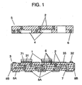
- a module component is described in accordance with a first exemplary embodiment of the present invention, referring to FIG. 1.
- the module component includes circuit substrate 3, a plurality of components 1 mounted on connection terminals 31 provided on one of the main surfaces of circuit substrate 3, and junction circuit substrate 5 having hollow 4 for fitting the mounted components 1 in.
- the junction circuit substrate is provided with a function of connecting both electrically and mechanically with circuit substrate 3.
- Circuit substrate 3 has wiring pattern 2, via 6 and through hole 7.
- Circuit substrate 3 is formed in the multi-layered wiring structure; two or more number of layers.
- Circuit substrate 3 is further provided on the upper surface with connection terminal 31 and connection terminal 32.
- Connection terminal 31 is for the connection with mounted component 1.
- Connection terminal 32 is for the electrical connection with via 6 of junction circuit substrate 5.
- the electric circuit in a module component is thus structured.
- Circuit substrate 3 is further provided with external connection terminals, 8A and 8B, for electrically connecting an individual module component with a mother board.
- Terminal 8A is provided in the LGA (Land Gurid Array) arrangement, where a number of terminal electrodes are formed on the lower surface of circuit substrate 3.
- Terminal 8B is provided as an end-face electrode, which is formed on the side face of circuit substrate 3.
- Circuit pattern 2 on the upper surface of circuit substrate 3 is additionally provided with constant adjustment pattern 33, which pattern playing the following role.
- the final electrical characteristics are sometimes optimized by adjusting the circuit constant of the circuit at the end stage of the manufacturing. It is not an easy job to adjust the electrical characteristics of circuit after component 1 is mounted within the inside.
- circuit constant adjustment function is added to circuit pattern 2 for meeting the above-described needs.
- Rectangular chip resistors, capacitors, inductors, EMC countermeasure components or the like passive components are mounted as component 1 on circuit substrate 3 by a high speed mounting facility. At the mounting operation, components 1 hit circuit substrate 3 with a certain force. The total mechanical shocks given to circuit substrate 3 during mounting procedure are substantial.
- circuit substrate 3 is made of a high rigidity material strong enough to withstand the mechanical shocks.
- the high-rigidity material includes FR-4, CEM-3 from the organic based materials, and a ceramic substrate, a metal substrate from the inorganic based materials.
- a cured composite resin substrate formed of a mixture containing inorganic filler and thermosetting resin can also be used.
- Components 1 are not limited to the passive components; packaged semiconductor ICs and other kinds of active components may be mounted as component 1.
- Chip LCRs, CSPs, etc. whose connection terminals are disposed at their bottom and side surfaces, FETs whose connection terminals are disposed at their bottom surface and the upper surface opposing to the bottom surface, and high frequency IC components whose surfaces other than connection terminal areas are covered with electrodes for the sake of heat dissipation or shielding can also be mounted as component 1.
- circuit substrate 3 is provided with connection terminals 31 compatible with such mounting components.
- components 1 are connected to circuit substrate 3 by means of soldering.
- a cream solder of Sn-Ag-Cu is applied using a 150 ⁇ m thick metal mask on terminal 31 in circuit substrate 3.
- Component 1 is placed on a predetermined place and connected and fixed by the reflow soldering, keeping the peak temperature 260°C for 5 seconds and then cooled.
- soldering flux In order to activate the surface of connection terminal 31 and to make the solder connection easy, a soldering flux is used. If the soldering flux remains after the soldering in the connected part, it will lead to a corrosion and connection failure, which leads to a significantly deteriorated reliability. In order to prevent this to happen, the remaining flux component is removed and cleaned using a cleaning agent containing isopropyl alcohol as the main ingredient. However, the residual flux staying in a very small gap of less than 200 ⁇ m between circuit substrate 3 and the mounted components 1 such as packaged IC, chip component is difficult to resolve and remove completely by simply immersing it in a cleaning agent. Therefore, an ultrasonic cleaning facility or a high speed fluid cleaner is used for a thorough removal of the flux.
- under-fill resin 71 formed of an epoxy resin and an inorganic filler material.
- the viscosity of under-fill resin 71 needs to be lowered. So, the entire circuit substrate 3 is heated to approximately 60°C before applying under-fill resin 71. And then, it is heated at 150°C for 5 min. for curing. This way of mounting the components eliminates the gap between circuit substrate 3 and mounted component 1, and high connecting reliability is ensured.
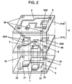
- Junction circuit substrate 5 is provided with hole 95A and hole 95B.
- Hole 95A is for fitting component 1 mounted on circuit substrate 3 in.
- Hole 95B is for fitting a trimmer capacitor or the like adjustment parts in. The capacitance is adjusted after a module component is finished; by trimming constant adjustment pattern 33 with a laser beam, Leutor, etc.
- Junction circuit substrate 5 is made of a thermosetting resin, a thermoplastic resin, etc.
- Preferred thermosetting resin includes a high heat-withstanding epoxy resin, a phenol resin, and a cyanate resin.
- the epoxy resin among other resins, has a significantly high heat-withstanding property; so it is advantageous in preventing the broken connection or short circuiting due to thermal distortion caused in junction circuit substrate 5 by the heat generated from mounted component 1.
- thermoplastic resin a highly heat-resistive polyimide, polyether sulfonate, etc. may be used.
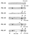
- a laminate sheet forming junction circuit substrate 5 is described. It is provided by forming a material containing thermosetting resin as the main ingredient into a sheet, as shown in FIG. 3A. Laminate sheet 91A, or 91B, is kept in the half-cured state (B stage) to be used as a prepreg.
- the presently used laminate sheet 91A, or 91B has a 500 ⁇ m thickness.
- the laminate sheet is provided with through holes at certain specified places.
- the through hole is filled with a conductive paste made of metal powder and resin using a combined method of screen printing and vacuum sucking process; via 92 is thus provided.
- wiring pattern 94 is formed on transfer-printing film 93.
- transfer-printing film 93 having wiring pattern 94 is laminated on the laminate sheet having via 92, and then heat-pressed.
- transfer-printing film 93 is removed. Wiring pattern 94 is thus provided on the laminate sheet.
- FIG. 3D transfer-printing film 93 having wiring pattern 94 is laminated on the laminate sheet having via 92, and then heat-pressed.
- transfer-printing film 93 is removed.
- Wiring pattern 94 is thus provided on the laminate sheet.
- a certain specific hole 95A, or 95B is provided.
- alignment hole 96 is also provided, which hole is used when laminating it with circuit substrate 3.
- Laminate sheet 91A, or 91B, which constitutes junction circuit substrate 5 is thus completed.
- a certain specific wiring pattern 2 is formed on laminate sheet 91A, or 91B, as shown in FIG. 2, by transfer-printing process.
- laminate sheet 91A is provided with hole 95A corresponding to mounted component 1, and hole 95B corresponding to constant adjustment pattern 33.
- Hole 95B is for trimming constant adjustment pattern 33 from outside after a module component is completed.
- Another laminate sheet 91B is provided with hole 95B corresponding to constant adjustment pattern 33.
- the holes in laminate sheet 91A, or 91B are formed by a laser beam facility. Since the facility uses a YAG laser beam, or an ultraviolet laser beam, whose wavelength is shorter than 2 ⁇ m, it generates less heat during the hole forming operation. As the result, it causes least thermal expansion/shrinkage at laminate sheet 91A, or 91B, enabling to form the holes at a high dimensional accuracy.
- the holes in laminate sheet 91A, or 91B, may be provided using a punching die, instead of using a laser beam facility.
- Laminate sheet 91A and laminate sheet 91B thus prepared are overlaid one after the other on circuit substrate 3.
- junction circuit substrate 5 having hollow 4 of desired depth and space that fit to the size of mounted component 1 can be provided.
- the overlaying operation is conducted while inserting a pin through alignment hole 81 of circuit substrate 3 and alignment hole 96 of junction circuit substrate 5.
- thermosetting resin for laminate sheet 91A, or 91B.
- Epoxy resin, polyimide resin, phenol resin, cyanate resin, etc. may be used.
- an inorganic filler may be added to the thermosetting resin. Silica, alumina, or ferrite may be used as the inorganic filler.
- junction circuit substrate 5 of high heat conductivity and high heat dissipation can be provided by adding high heat conductivity alumina in laminate sheet 91A, or 91B. Junction circuit substrate 5 thus provided and circuit substrate 3 are integrated together by heat pressing them at 150 - 200°C, pressing force 100 - 200 kg/cm 2 . Since the thermosetting resin at this step is in the half-cured state (B stage), junction circuit substrate 5 formed of laminate sheet 91A, or 91B, is once softened and then cured. Location of connection terminal 32 on the upper surface of circuit substrate 3 precisely coincides with via 6 formed in junction circuit substrate 5, as shown in FIG. 2. Circuit substrate 3 and junction circuit substrate 5 are electrically connected by heat-compressing the conductive paste which is filling via 6.
- connection terminal 32 may be provided in junction circuit substrate 5, while via 6 in circuit substrate 3, for implementing the same purpose.
- connection terminal 32 may be provided in junction circuit substrate 5, while via 6 in circuit substrate 3, for implementing the same purpose.
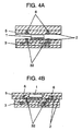
- junction circuit substrate 5 when junction circuit substrate 5 is heat-pressed, wiring pattern 2 and via 6 formed in junction circuit board 5 are transformed and displaced freely in the horizontal direction, in proportion to the volume of mounted component 1.
- thermosetting resin of junction circuit substrate 5 in the state of B stage gets softened.
- the precise wiring pattern 2 is originally located so that it can establish electrical contact with via 6 of junction circuit substrate 5 and connection terminal 32 on circuit substrate 3.
- wiring pattern 2 and via 6 are dislocated by the deformation and the free movement.
- the deformation and free movement caused as the result of the softened junction circuit substrate 5 at the time of integration makes it impossible to accomplish a high precision connection.
- shape of the pattern and the via for connection needs to be enlarged to be large enough to cover the amount of dislocation due to deformation and movement. Then, a circuit can not be formed within a certain desired substrate area, rendering the down-sizing of a module component difficult.
- the pressure concentrating to mounted component 1 might destroy the component.
- junction circuit substrate 5 is provided with hollow 4 for fitting mounted component 1 in, as shown in FIG. 5A, it eliminates the deformation and free movement of thermosetting resin, which would have otherwise been caused for the amount corresponding to the volume of mounted component 1. Furthermore, since component 1 mounted and fixed on circuit substrate 3, it plays the role of a bulwark to prevent the deformation/movement of wiring pattern 2 and via 6. Thus, it regulates the dislocation of wiring pattern 2 and via 6, and the high precision connection as shown in FIG. 5B can be implemented for the downsizing of a module component.
- the dimensional allowance between hollow 4 and component 1 is less than 1% of the length, width and height of component 1. By so doing, the dislocation of wiring pattern 2 can be eliminated. Furthermore, since there is no concentrated pressure on mounted component 1, a possible damage on component 1 can be avoided. Thus, it provides the module components with a high reliability.
- circuit substrate 3 and junction circuit substrate 5 are heated for integration, respective materials of circuit substrate 3 and junction circuit substrate 5 are substantially identical in the thermal expansion coefficient. As the result, the dislocation due to expansion/shrinkage of substrates can be eliminated, which helps implementing smaller and higher-precision module components.
- circuit substrate 3 and junction circuit substrate 5 are integrated as shown in FIG. 6A, mounted components 1 are completely sealed without an air gap.
- hole 95B allows an additional adjustment operation to be made thereafter from the outside on constant adjustment pattern 33.
- the circuit constant of electrical circuit can be adjusted even after a module component is completed, by using a laser beam, Leutor, etc. After the adjustment operation, the module component is finally sealed, as shown in FIG. 6A, with sealing material 11 containing an epoxy resin as the main ingredient.
- the module components completely sealed without an air gap exhibit a high reliability in the moisture absorption reflow test. If the laminated circuit substrate 3 and junction circuit substrate 5 had an air gap, the JEDEC moisture absorption reflow test conducted at the Level 1 condition result in water in the air gap.
- the moisture absorption conditions specified in JEDEC Reflow Level 1 are; for 168 hours in 85°C, 85% RH.
- the module components sealed in accordance with the present invention without an air gap can survive the Level 1 moisture absorption reflow test, exhibiting no breakage. The high reliability is maintained.
- the average surface roughness (Ra) of circuit substrate 3 Prior to integration of circuit substrate 3 and junction circuit substrate 5, the average surface roughness (Ra) of circuit substrate 3 is made to be more than 10 ⁇ m.
- junction surface of junction circuit substrate 5 can get a firm grip into the roughened surface of circuit substrate 3, to an enhanced adhesive strength between circuit substrate 3 and junction circuit substrate 5.
- protruding electrode 64 is formed on connection terminal 62 of junction circuit substrate 5.
- a gold stud bump of melted gold wire formed with the help of an ultrasonic wave on connection terminal 62, or a Ni-Au bump formed by either electrolytic plating or electroless deposition serves as protruding electrode 64.
- Protruding electrode 64 and Ni-Au plated connection terminal 32 disposed on circuit substrate 3 accomplish the Au-Au metal bond by the heat and the pressure. This implements a surer and lower-resistance connection. Instead, a solder connection is a possibility; using solder bumps formed with a certain fixed amount of melted solder.
- a module component in the present invention is formed by laminating junction circuit substrate 5 on circuit substrate 3, and the area of circuit substrate 3 is identical to or larger than junction circuit substrate 5.
- junction circuit substrate 5 can be laminated on circuit substrate 3 with ease, which leads to a higher productivity in the manufacture.
- circuit substrate 3 may be provided at the upper surface with wall 51 for placement regulation.
- the wall 51 prevents wiring pattern 2 and via 6 of junction circuit board 5 from making a free movement on the surface. This enables to maintain a high accuracy in the dimensions of connection.
- the size of hollow 4A of junction circuit substrate 5 is identical to or slightly smaller than the shape of mounted component 1. As the result, mounted component 1 is press-fit tightly with hollow 4A. In this way, there is no gap between mounted component 1 and junction circuit substrate 5, and the connection reliability is improved.
- the size of hollow 4A can be identical to or larger than that of mounted component 1, as shown in FIG. 9B. This makes the laminating operation easier.
- the gap existing between hollow 4A and mounted component 1 is filled while a pressure is given for lamination.
- elastic member 102 is provided on the wall surface of hollow 4A, for filling the gap between mounted component 1 and wall surface of hollow 4A. As a result, the outside air can be totally blocked, and the gap with mounted component 1 is filled. This can further improve the reliability at the moisture absorption reflow test, etc.
- the elastic member a silicone rubber, a fluoro rubber, etc. may be used. Or, as shown in FIG.
- hollow 4B may take a trapezoid form in the cross sectional shape, with the mouth broader.
- the trapezoid form makes the aligning at the fitting operation of mounted component 1 with hollow 4B easier.
- FIG. 9A - FIG. 9D exhibit variations of hollow 4A and 4B in their cross sectional shapes. The above concepts of variation are applicable also to such cases where hole is formed, besides hollow 4A, 4B.
- Junction circuit substrate 5 in the present embodiment 1 has been described based on a resin substrate using prepreg. However, other high-rigidity substrate may be used for junction circuit substrate 5, with a connection layer provided at the junction surface of junction circuit substrate 5 and circuit substrate 3.
- the substrates are integrated into a single body by curing the connection layer with a heat, a pressure or an energy beam; and a finished module component is completed.
- the energy beam includes an electron beam, X-ray beam and a radiation beam, etc.
- the high-rigidity substrate includes a cured resin substrate, a ceramic substrate, a metal substrate and a composite resin substrate made of a mixture containing inorganic filler and thermosetting resin, and cured, and others.
- a preferred inorganic filler is alumina. Since these ceramic substrates, metal substrates, composite resin substrates containing alumina as the main ingredient are provided with a high thermal conductivity, they can effectively radiate the heat generated from the heat-generating component 1.
- junction circuit substrate 5 and circuit substrate 3 are connected by means of an adhesive layer.
- Junction circuit substrate 5 shown in FIG. 10A is a multi-layered ceramic substrate. The inner layer of which substrate is provided with via 6 for the layer-to-layer electrical connection.
- hollow 4 Provided at the lower surface of junction circuit substrate 5 are hollow 4 which corresponds to mounted component 1 and connection terminal 62 which is slightly pushing out of the lower surface for electrical connection with circuit substrate 3.
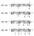
- adhesive layer 65 is provided as shown in FIG. 10B.
- Adhesive layer 65 is formed by applying an adhesive agent which contains an epoxy resin as the main ingredient.
- connection terminal 62 establishes an electrical connection with connection terminal 32 of circuit substrate 3 by breaking adhesive layer 65 through.
- FIG. 10C when providing adhesive layer 65 on the exposed surface of junction circuit substrate 5, the area of connection terminal 62 which makes contact with circuit substrate 3 may be excluded. By so doing, the reliability in the connection with circuit substrate 3 is improved.
- adhesive layer 65 may be formed evading connection terminal 62 of junction circuit substrate 5, while conductive layer 63 is provided on connection terminal 62. This structure further improves the connection reliability.
- Conductive layer 63 is formed by applying a conductive paste.
- the adhesive agent a two-liquid type adhesive or an anaerobic adhesive may be used. Besides the liquid adhesives, an adhesive agent in the form of an adhesive sheet can be used.
- connection resistance is reduced a step further.
- the conductive layer provided at the open region realizes another reduction in the connection resistance.
- Component 1 can be mounted on circuit substrate 3 with a solder or a conductive paste.
- a solder or a conductive paste for mounting a semiconductor bear chip, among other components, there are two mounting methods; viz. connecting at a relatively low temperature using an anisotropic conductive resin sheet or a conductive paste, or connecting at a high temperature using a solder or gold.
- the flatness of circuit substrate 3 at the surface of connection area, where the bare chip is mounted is to be less than 10 ⁇ m.
- the solder mounting method is suitable to volume production, so it is often used.
- connection terminals 31 are disposed in accordance with the pitch of solder bumps 20.
- the pitch is very small as shown in FIG. 11B, therefore a melted solder sometimes flows out of the own connection terminal to reach other terminals. This leads to short-circuiting between the connection terminals, and makes it difficult to maintain certain predetermined electrical characteristics.
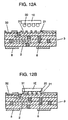
- circuit substrate 3 is provided with walls between respective connection terminals 31, as shown in FIG. 12A, which walls being made of resist 21 formed of a resin as the main ingredient.
- the wall of resist 21 is provided also in other areas than connection terminal 32. As shown in FIG. 12, resist 21 is needed to prevent the solder from flowing on wiring pattern 2.
- resist 21 is provided on circuit substrate 3 in the above descriptions, it can also be provided with respect to wiring pattern 2 formed on junction circuit substrate 5.
- Hollow 4 of junction circuit substrate 5 may be provided at the bottom surface 12 with terminal 111, as shown in FIG. 13A.
- An FET and the like component 1 having its terminal 112 at the opposing surface can be connected electrically by making use of terminal 111.
- the electrical connection between terminal 111 and terminal 112 of mounted component 1 may be accomplished by a pressure connection. When a conductive layer or an anisotropic conductive sheet is provided on terminal 112, the electrical connection is implemented at a still lower resistance.
- Hollow 4 of junction circuit substrate 5 may be provided at the side surface with terminal 113, as shown in FIG. 13B. This enables component 1 to establish electrical contact at its side-face electrode 114 with terminal 113. In this way, junction circuit substrate 5 can be connected direct with mounted component 1, not via circuit substrate 3. Furthermore, as shown in FIG. 13C, hollow 4 of junction circuit substrate 5 may be provided in the inside with shield layer 115 formed of gold, copper or other conductive material. This helps suppress the influence of noise generated from mounted component 1 to a minimum level. Still further, as shown in FIG. 13D, hollow 4 of junction circuit substrate 5 may be provided at the bottom surface 12 with heat conductive layer 116 of copper or the like metal. Component 1 having its heat radiation layer at the portion other than the place of connection terminal, e.g.
- Description in the present embodiment 1 has been based on the process of manufacturing module components piece-by-piece.
- a number of module components 141 can be manufactured altogether at once, as shown in FIG. 14, to be separated later into individual module components.
- the thermal expansion coefficient of circuit substrate 3 should preferably be identical to that of junction circuit substrate 5.
- both substrates have substantially the same thermal expansion coefficient, possible warp of a module component that would arise at the reflow connection with the mother substrate can be suppressed. Namely, the bending stress is reduced, and breakage and short-circuiting of wiring pattern 2 can be eliminated.
- hollow 4 has been provided for fixing one individual component 1 each.
- one hollow 4 may house a plurality of components 1 which have been disposed in proximity to each other.
- module component containing mounting components in accordance with the present invention is described.
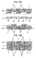
- junction circuit substrate 5 is configured to have hollow 4A which corresponds to component 1 mounted on circuit substrate 3A, and hollow 4B which corresponds to component 1 mounted on circuit substrate 3B.
- Components 1 on respective circuit substrates 3A and 3B are mounted so that each of them does not overlap with the one on other circuit substrate at the same location. In this way, respective components 1 on the two circuit substrates are eventually disposed flat in the same level.
- wiring pattern 2 finer.
- wiring pattern 2 is extended around here and there, and a number of mounting components 1 is disposed densely on the surface of circuit substrate 3.
- the number of vias 6 inevitably increases, so is the number of lamination layers.
- mechanical strength of circuit substrate 3 deteriorates, while the increased layer counts increases the thickness. Namely, the downsizing target is not implemented through the conventional procedures.
- circuit substrate 3A and circuit substrate 3B are disposed respectively at the up and down of junction circuit substrate 5, the density of mounting components 1 can be raised using the already existing wiring rules. Furthermore, thickness of module components can be reduced; which is an additional advantage for making the height of an apparatus lower.
- no component has been mounted on the surface of circuit substrates 3A, 3B reverse to that facing to junction circuit substrate 5; however, the reverse surfaces may of course be mounted with components 1.
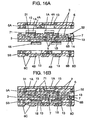
- Embodiment 3 in the present invention is described referring to FIG. 16A and FIG. 16B.
- a module component in embodiment 3 is an example in which analog circuit and digital circuit are incorporated together.
- Circuit substrate 3 is mounted at the upper surface with components 1A forming an analog circuit.
- Circuit substrate 3 is mounted at the lower surface with components 1B forming a digital circuit.
- shield layer 13 and ground electrode 14 are provided in the inside of circuit substrate 3.
- Junction circuit substrate 5A has hollows 4A which correspond to components 1A mounted on the upper surface of circuit substrate 3.
- Junction circuit substrate 5B has hollows 4B which correspond to components 1B mounted on the lower surface of circuit substrate 3.
- Shield layer 13 is formed on the surface of hollow 4B.
- Junction circuit substrate 5B is provided with connection terminals 8C and 8D for electrical connection with the mother substrate. Among the connection terminals, terminal 8D is connected with the GND electrode of mother substrate. Connection terminal 8D is further connected with ground electrode 14 of circuit substrate 3 by way of via 6B.
- the method of lamination remains the same as in embodiment 1.
- analog circuit and digital circuit are disposed on the upper and the lower surfaces, respectively, of one circuit substrate 3
- digital signal can be overlaid as noise on analog signal, which would lead to an operation error. Therefore, the digital circuit needs to be shielded so that no digital signal escapes as noise. While in the analog circuit, it is important to protect itself against noise by means of shielding, for keeping the reliability of the signal it processes.
- each of the circuits has to be shielded by means of metal shield case.
- metal shield case the size of a module component inevitably goes big.
- the circuits are disposed on the upper surface and the lower surface, respectively, of circuit substrate 3, it is needed to have the shield case both on the upper and the lower surfaces.
- the terminal for connection with mother substrate needs to be disposed somewhere in the area having no shield case. As the result, the total structure of a module component becomes complicated.
- shield layer 13 is formed within circuit substrate 3, as well as on the inner surface of hollows 4A, 4B of junction circuit substrates 5A, 5B.
- the respective analog circuit and the digital circuit can be shielded.
- the size of module component does not go bigger, and the terminal for connection with mother substrate can be disposed at the lower surface of junction circuit substrate 5B.
- Shield layer 13 formed in circuit substrate 3 as the reference GND for respective circuits, and the GND potential of mother substrate are brought to the same level.
- the circuits formed on circuit substrate 3 can be kept to be free of parasitic LCR; and the reliability of electric signals can be ensured.
- a compact module component is offered in accordance with the present invention, where the electrical characteristics are not deteriorated even when analog circuit and digital circuit are disposed together.
- Circuit substrate 3 may be formed of a laminate substrate of different materials, or an integration of a ceramic substrate and a composite resin substrate. If the composite resin substrate is formed of ferrite and ceramic as the inorganic filler, it removes the noises from mounted component 1 and circuit pattern 2. Namely, since the circuit substrate 3 can separate the electric circuits electrically, it can be used as a circuit substrate 3 having the shielding effects.
- laminate substrate of different materials is an integration of composite resin substrates, where each one composite resin substrate containing an inorganic filler consisting of either one of the high dielectric constant material, the low dielectric constant material and the ferrite material.
- a laminate body having various dielectric constant and magnetic permeability is used, a chip capacitor, a resistor, a coil, etc. which used to be mounted on the circuit substrate can be formed within the inside of the laminate body. As the result, the size of a module component can be made smaller.
- circuit substrate 3 has been formed in a laminate substrate of different materials, the same idea can be applied to junction circuit substrate 5.
- FIG. 17A and FIG. 17B A module component in accordance with embodiment 4 is described referring to FIG. 17A and FIG. 17B.
- Components 1A and 1B are mounted on the lower surface of circuit substrate 3.
- Junction circuit substrate 5 is provided with hollows 4A and 4B corresponding to mounted components 1A and 1B.
- junction circuit substrate 5 is provided at the bottom of hollow 4B with via 6C, and a metal body of high thermal capacitance such as copper, aluminum, etc. is buried in part of junction circuit substrate 5 as heat radiation member 15 in a manner that it makes contact with via 6C. Under this configuration, the high temperature generated at a certain part of mounted component 1B is conveyed through via 6C formed in junction circuit substrate 5 to heat radiation member 15 to be efficiently conducted to external connection terminal 8A. Thus, the heat is quickly discharged to the outside.
- terminal 8A of LGA structure and terminal 8B of side face electrode are disposed on circuit substrate 3. In the present embodiment 4, these are disposed on junction circuit substrate 5.
- FIG. 17B shows a module component of high heat-discharging capability having its heat radiation member 15 in junction circuit substrate 5.
- Another high heat-discharging module component can be configured by disposing heat radiation member 15 in circuit substrate 3, as shown in FIG. 18A and FIG. 18B.
- Circuit substrate 3 may be formed using a cured resin substrate, a ceramic substrate containing heat-conductive alumina as the main ingredient, a metal substrate, a cured composite resin substrate, etc. In this way, the heat of component 1B, which generates a substantial amount of heat, can be discharged efficiently so that the power supply IC can operate to the full performance.
- Circuit substrate 3A is provided at the upper and the lower surfaces with components 1A forming a digital circuit.
- Junction circuit substrate 5A is provided with hollows 4A corresponding to components 1A mounted on the upper surface of circuit substrate 3A.
- Junction circuit substrate 5A is provided at the upper surface with shield layer 13.
- Junction circuit substrate 5B is provided with hollows 4A corresponding to components 1A mounted on circuit substrate 3A at the lower surface.
- Junction circuit substrate 5B is proved with connection terminals 8C and 8D for electrical connection with the mother substrate.
- Connection terminal 8D is connected with the GND electrode of mother substrate.
- Circuit substrate 3B is provided at the upper surface with a plurality of components 1B disposed adjacent to each other, also component 1B at the lower surface. Thus circuit substrate 3B constitutes an analog circuit.
- Junction circuit substrate 5D is provided with hollow 4B, which hollow corresponding to the plurality of components 1B mounted on the upper surface of circuit substrate 3B.
- Junction circuit substrate 5C is provided with hollow 4B, which hollow corresponding to component 1B mounted on the lower surface of circuit substrate 3B.
- Hollow 4B is provided on the surface with shield layer 13.
- Lamination method remains the same as in embodiment 1.
- a method of forming different kinds of circuits within a module component has already been described in embodiment 3.
- junction circuit substrates and circuit substrates may be used for lamination, as described in the present example.
- the present embodiment 5 described an exemplary structure where a circuit substrate sandwiched by junction circuit substrates is combined for two sets.
- the structure of a module component is not limited to the above-described; there can be a number of variations in the combination of junction circuit substrates and circuit substrates.
- the present invention teaches an improved reliability implemented through a higher accuracy in the dimensions, a reduction of damage on substrate which is caused by the shocks given by components when they are mounted, a reduced warp in a laminated substrate which is caused by the difference in the thermal expansion coefficient.
- a compact module component containing components within the inside is offered accompanied by an improved operational reliability.
- the present invention can implement and offer compact size module components containing within the inside a plurality of components mounted at a high precision level with a high mounting density. These module components exhibit a high reliability in the layer-to-layer connection.
Landscapes
- Engineering & Computer Science (AREA)
- Manufacturing & Machinery (AREA)
- Microelectronics & Electronic Packaging (AREA)
- General Engineering & Computer Science (AREA)
- Physics & Mathematics (AREA)
- General Physics & Mathematics (AREA)
- Combinations Of Printed Boards (AREA)
- Production Of Multi-Layered Print Wiring Board (AREA)
- Structures For Mounting Electric Components On Printed Circuit Boards (AREA)
Abstract
Description
Claims (72)
- A module component comprising
one or more mounting components,
a circuit substrate having the components mounted on at least one of the surfaces, and
a junction circuit substrate having either a hollow or a hole at the places corresponding to the components mounted on the one surface of circuit substrate for fitting the mounted components in, wherein
the junction circuit substrate is provided with a connecting function, the circuit substrate and the junction circuit substrate are laminated into a single body and then cured so that the mounted components are contained within the module component. - A module component comprising
one or more mounting components,
one circuit substrate having the components mounted on at least one of the surfaces,
another circuit substrate having the components mounted on at least one of the surfaces, and
a junction circuit substrate disposed between the circuit substrates, which junction circuit substrate having either a hollow or a hole at the places corresponding to the components mounted on the opposing surfaces of the respective circuit substrates for fitting the components in, wherein
the junction circuit substrate is provided with a connecting function, the respective circuit substrates and the junction circuit substrate are laminated into a single body and then cured so that the mounted components are contained within the module component. - A module component comprising
one or more mounting components,
a circuit substrate having the components mounted on at least one of the surfaces, and
one junction circuit substrate having either a hollow or a hole at the places corresponding to the one or more components mounted on circuit substrate for fitting the mounted components in, wherein
the junction circuit substrate is provided with a connecting function, the circuit substrate is sandwiched by the one junction circuit substrate and another junction circuit substrate to be laminated into a single body and then cured so that the mounted components are contained within the module component. - A module component formed by laminating two or more of any module components recited in one of claims 1 through 3, wherein
at least the junction surface is provided by either a combination of the circuit substrate and the junction circuit substrate, or a combination of the junction circuit substrates. - The module component of claim 4, wherein
the junction circuit substrate disposed between the circuit substrates is provided on both surfaces with a hollow or a hole for fitting the components mounted on the opposing circuit substrates in. - The module component recited in one of claims 1 through 3, wherein the mounted component is provided with a heat radiation member.
- The module component recited in one of claims 1 through 3, wherein the mounted component is provided on at least one of the surfaces with a connection terminal.
- The module component recited in one of claims 1 through 3, wherein the mounted component is provided with connection terminals on the two opposite surfaces.
- The module component recited in one of claims 1 through 3, wherein the mounted component is provided with a shielding surface on all of the surfaces with the exception of one surface.
- The module component recited in one of claims 1 through 3, wherein the circuit substrate is provided with at least one item selected from the group of through hole, via and wiring pattern.
- The module component recited in one of claims 1 through 3, wherein the circuit substrate and the junction circuit substrate are electrically connected by at least one means selected from the group of through hole, via and wiring pattern.
- The module component recited in one of claims 1 through 3, wherein the circuit substrate has an average surface roughness 10µm, or more.
- The module component recited in one of claims 1 through 3, wherein the circuit substrate is provided with an external connection terminal.
- The module component of claim 13, wherein the external connection terminal is formed in either the LGA or a side-face electrode structure.
- The module component recited in one of claims 1 through 3, wherein the circuit substrate is formed of a material which is provided with the function for suppressing the thermal shrinkage of the junction circuit substrate caused during the lamination process for integration.
- The module component of claim 15, wherein the circuit substrate is formed of at least one item selected from the group of cured resin substrate, ceramic substrate, metal substrate and cured composite resin substrate.
- The module component recited in one of claims 1 through 3, wherein the circuit substrate is provided with a heat radiating function.
- The module component recited in one of claims 1 through 3, wherein the circuit substrate is provided with at least either a layer-to-layer shielding function or a partial shielding function.
- The module component recited in one of claims 1 through 3, wherein the circuit substrate has an electric circuit which contains at least one item among the group of inductor, capacitor, resistor, filter, IC and adjustment circuit.
- The module component recited in one of claims 1 through 3, wherein the circuit substrate has a multi-layered wiring structure of either the layer-to-layer bond or the layer-to-layer connection.
- The module component recited in one of claims 1 through 3, wherein the circuit substrate has a connection terminal for connection with the junction circuit substrate.
- The module component recited in one of claims 1 through 3, wherein the circuit substrate has an anti-solder drift wall in part of connection terminal land.
- The module component recited in one of claims 1 through 3, wherein the circuit substrate has an area identical to, or larger than, the junction circuit substrate.
- The module component recited in one of claims 1 through 3, wherein the circuit substrate is formed of a laminated body of different materials.
- The module component recited in one of claims 1 through 3, wherein the circuit substrate is provided with a thermal conductivity.
- The module component of claim 25, wherein the circuit substrate is incorporating a heat radiation member.
- The module component recited in one of claims 1 through 3, wherein the circuit substrate has a thermal expansion coefficient that is substantially identical to that of the junction circuit substrate.
- The module component recited in one of claims 1 through 3, wherein the circuit substrate is provided with a function of removing electrical noise.
- The module component recited in one of claims 1 through 3, wherein the circuit substrate is incorporating the ground electrode.
- The module component recited in one of claims 1 through 3, wherein the circuit substrate is provided with an wall for alignment.
- The module component recited in one of claims 1 through 3, wherein at least either one of the circuit substrate and the junction circuit substrate is provided at the junction surface with a protrusion, or a hole, for alignment.
- The module component recited in one of claims 1 through 3, wherein the circuit substrate is provided with a function of adjusting the constant of electrical characteristic.
- The module component recited in one of claims 1 through 3, wherein the junction circuit substrate is provided with at least one item selected from the group of through hole, via and wiring pattern.
- The module component recited in one of claims 1 through 3, wherein the junction circuit substrate has an external connection terminal.
- The module component of claim 34, wherein the external connection terminal is formed in either the LGA or a side-face electrode structure.
- The module component recited in one of claims 1 through 3, wherein the mounted component is press-fit to the hollow, or the hole, of the junction circuit substrate.
- The module component recited in one of claims 1 through 3, wherein the hollow, or the hole, of the junction circuit substrate has a size which can absorb the dimensional allowance not more than 1% of the mounted component.
- The module component recited in one of claims 1 through 3, wherein the hollow, or the hole, of the junction circuit substrate has a shape which is larger at the mouth for fitting-in the mounted component than the size in the inside.
- The module component recited in one of claims 1 through 3, wherein the junction circuit substrate is provided with a terminal at the bottom of hollow.
- The module component recited in one of claims 1 through 3, wherein the junction circuit substrate is provided with a terminal at the side wall of hollow, or hole.
- The module component recited in one of claims 1 through 3, wherein the junction circuit substrate is provided with a shield layer in the hollow, or hole.
- The module component recited in one of claims 1 through 3, wherein the junction circuit substrate is provided with a conductive layer in the hollow, or the hole.
- The module component recited in one of claims 1 through 3, wherein the junction circuit substrate is provided with an elastic layer in the hollow, or hole.
- The module component recited in one of claims 1 through 3, wherein the junction circuit substrate is provided with a heat conductive layer in the hollow, or hole.
- The module component recited in one of claims 1 through 3, wherein the junction circuit substrate is formed of a prepreg.
- The module component recited in one of claims 1 through 3, wherein the junction circuit substrate is provided with an adhesive layer at the surface.
- The module component of claim 46, wherein the adhesive layer is formed by applying an adhesive agent of either two-liquid type or anaerobic type.
- The module component of claim 46, wherein the adhesive layer is patterned to have a void at the region corresponding to an area where the circuit substrate and the junction circuit substrate are electrically connected.
- The module component of claim 48, wherein the region void of adhesive layer is filled with an electro conductive paste.
- The module component of claim 46, wherein the adhesive layer is formed of an adhesive sheet.
- The module component of claim 50, wherein the adhesive sheet is provided with a void hole at the region corresponding to an area where the circuit substrate and the junction circuit substrate are electrically connected.
- The module component of claim 51, wherein the void hole of adhesive sheet is filled with an electro conductive paste.
- The module component of claim 50, wherein the adhesive sheet is provided with conductive particles.
- The module component recited in one of claims 1 through 3, wherein the junction circuit substrate is formed of either a thermosetting resin or a thermoplastic resin.
- The module component of claim 46, wherein the junction circuit substrate is formed of either a thermosetting resin or a thermoplastic resin.
- The module component of claim 46, wherein the junction circuit substrate is formed of a material which does not cause a dimensional change when the adhesive layer is cured.
- The module component of claim 56, wherein the junction circuit substrate is formed of at least one item among the group of cured resin substrate, ceramic substrate, metal substrate and cured composite resin substrate.
- The module component recited in one of claims 1 through 3, wherein the junction circuit substrate is provided with a heat radiating function.
- The module component recited in one of claims 1 through 3, wherein the junction circuit substrate is provided with at least either a layer-to-layer shielding function or a partial shielding function.
- The module component recited in one of claims 1 through 3, wherein the junction circuit substrate has an electric circuit which contains at least one item among the group of inductor, capacitor, resistor, filter, IC and adjustment circuit.
- The module component recited in one of claims 1 through 3, wherein the junction circuit substrate has a multi-layered wiring structure of either the layer-to-layer bond or the layer-to-layer connection.
- The module component recited in one of claims 1 through 3, wherein the junction circuit substrate a connection terminal for connection with the junction circuit substrate.
- The module component recited in one of claims 1 through 3, wherein the junction circuit substrate has an anti-solder drift wall in part of connection terminal land.
- The module component recited in one of claims 1 through 3, wherein the junction circuit substrate is formed of a laminated body of different materials.
- The module component recited in one of claims 1 through 3, wherein the junction circuit substrate is provided with a thermal conductivity.
- The module component of claim 65, wherein the junction circuit substrate is incorporating a heat radiation member.
- The module component recited in one of claims 1 through 3, wherein the junction circuit substrate is provided with a function of removing electrical noise.
- The module component recited in one of claims 1 through 3, wherein the junction circuit substrate is incorporating the ground electrode.
- The module component recited in one of claims 1 through 3, wherein connection terminal of either the circuit substrate or the junction circuit substrate is protruding to the opponent side.
- The module component recited in one of claims 1 through 3, wherein the portion containing the mounted component has no air gap.
- The module component recited in one of claims 1 through 3, wherein no air gap exists between the mounted component and the circuit substrate at the mounted surface.
- The module component of claim 71, wherein air gap between the mounted component and the circuit substrate at the mounted surface is filled with a resin.
Applications Claiming Priority (3)
| Application Number | Priority Date | Filing Date | Title |
|---|---|---|---|
| JP2002041066 | 2002-02-19 | ||
| JP2002041066A JP2003243797A (en) | 2002-02-19 | 2002-02-19 | Module parts |
| PCT/JP2003/001785 WO2003071603A1 (en) | 2002-02-19 | 2003-02-19 | Module part |
Publications (2)
| Publication Number | Publication Date |
|---|---|
| EP1478023A1 true EP1478023A1 (en) | 2004-11-17 |
| EP1478023A4 EP1478023A4 (en) | 2008-12-31 |
Family
ID=27750457
Family Applications (1)
| Application Number | Title | Priority Date | Filing Date |
|---|---|---|---|
| EP03705323A Withdrawn EP1478023A4 (en) | 2002-02-19 | 2003-02-19 | MODULE PIECE |
Country Status (5)
| Country | Link |
|---|---|
| US (2) | US7161371B2 (en) |
| EP (1) | EP1478023A4 (en) |
| JP (1) | JP2003243797A (en) |
| CN (1) | CN100472779C (en) |
| WO (1) | WO2003071603A1 (en) |
Cited By (9)
| Publication number | Priority date | Publication date | Assignee | Title |
|---|---|---|---|---|
| WO2010012594A1 (en) * | 2008-07-31 | 2010-02-04 | Robert Bosch Gmbh | Printed circuit board with electronic component |
| EP1648028A4 (en) * | 2004-06-10 | 2010-05-26 | Panasonic Corp | COMPOSITE ELECTRONIC COMPONENT |
| US7943001B2 (en) | 2006-06-16 | 2011-05-17 | Fujitsu Limited | Process for producing multilayer board |
| WO2011066106A1 (en) * | 2009-11-24 | 2011-06-03 | Marvell World Trade Ltd. | Embedded chip packages |
| US8400776B2 (en) | 2006-07-28 | 2013-03-19 | Dai Nippon Printing Co., Ltd. | Multilayered printed wiring board |
| US8455769B2 (en) | 2008-01-30 | 2013-06-04 | Murata Manufacturing Co., Ltd. | Electronic component and method of mounting the same |
| ITMI20121134A1 (en) * | 2012-06-27 | 2013-12-28 | St Microelectronics Srl | FLIP CHIP ELECTRONIC DEVICE AND RELATED PRODUCTION METHOD |
| EP2940729A1 (en) * | 2014-04-28 | 2015-11-04 | AT & S Austria Technologie & Systemtechnik Aktiengesellschaft | Electronic assembly comprising a carrier structure made from a printed circuit board |
| EP2985785A4 (en) * | 2013-04-10 | 2017-01-11 | Mitsubishi Electric Corporation | Semiconductor device and semiconductor device manufacturing method |
Families Citing this family (53)
| Publication number | Priority date | Publication date | Assignee | Title |
|---|---|---|---|---|
| JP2003243797A (en) * | 2002-02-19 | 2003-08-29 | Matsushita Electric Ind Co Ltd | Module parts |
| JP2005108625A (en) | 2003-09-30 | 2005-04-21 | Jst Mfg Co Ltd | Multi-layer anisotropic conductive sheet |
| JP4287733B2 (en) * | 2003-11-04 | 2009-07-01 | 日本シイエムケイ株式会社 | Multi-layer printed wiring board with built-in electronic components |
| JP2005158770A (en) * | 2003-11-20 | 2005-06-16 | Matsushita Electric Ind Co Ltd | LAMINATED BOARD, MANUFACTURING METHOD THEREOF, MODULE MANUFACTURING METHOD USING THE LAMINATED SUBSTRATE AND ITS MANUFACTURING DEVICE |
| CN1774965A (en) * | 2004-03-30 | 2006-05-17 | 松下电器产业株式会社 | Module component and method for manufacturing the same |
| JP4251144B2 (en) * | 2004-04-19 | 2009-04-08 | パナソニック株式会社 | Manufacturing method of laminated substrate |
| JP4218576B2 (en) * | 2004-04-19 | 2009-02-04 | パナソニック株式会社 | Manufacturing method of laminated substrate |
| JP4792749B2 (en) * | 2005-01-14 | 2011-10-12 | 大日本印刷株式会社 | Manufacturing method of printed wiring board with built-in electronic components |
| EP1863087A4 (en) * | 2005-03-17 | 2010-12-22 | Panasonic Corp | Module board |
| US7935892B2 (en) * | 2005-04-14 | 2011-05-03 | Panasonic Corporation | Electronic circuit device and method for manufacturing same |
| JP4215024B2 (en) * | 2005-04-22 | 2009-01-28 | パナソニック株式会社 | Manufacturing method of laminated substrate |
| JP4417294B2 (en) * | 2005-06-16 | 2010-02-17 | パナソニック株式会社 | Probe card component built-in substrate and manufacturing method thereof |
| DE102005032489B3 (en) * | 2005-07-04 | 2006-11-16 | Schweizer Electronic Ag | Circuit board multi-layer structure with integrated electric component, has insert embedded between two flat electrically insulating liquid resin structures |
| JP4175351B2 (en) * | 2005-08-26 | 2008-11-05 | 松下電工株式会社 | Uneven multilayer circuit board module and manufacturing method thereof |
| JP2007158157A (en) * | 2005-12-07 | 2007-06-21 | Alps Electric Co Ltd | Electronic circuit device |
| US20100153836A1 (en) * | 2008-12-16 | 2010-06-17 | Rich Media Club, Llc | Content rendering control system and method |
| JP4849926B2 (en) * | 2006-03-27 | 2012-01-11 | 富士通株式会社 | Semiconductor device and manufacturing method of semiconductor device |
| JP5034289B2 (en) * | 2006-03-28 | 2012-09-26 | 大日本印刷株式会社 | Multilayer printed wiring board and manufacturing method thereof |
| SG139594A1 (en) * | 2006-08-04 | 2008-02-29 | Micron Technology Inc | Microelectronic devices and methods for manufacturing microelectronic devices |
| KR100763345B1 (en) | 2006-08-30 | 2007-10-04 | 삼성전기주식회사 | Manufacturing Method of Electronic Circuit Board |
| JP4939916B2 (en) * | 2006-12-21 | 2012-05-30 | 株式会社フジクラ | Multilayer printed wiring board and manufacturing method thereof |
| JP4970994B2 (en) * | 2007-03-19 | 2012-07-11 | ルネサスエレクトロニクス株式会社 | Semiconductor package |
| EP2136610A4 (en) * | 2008-01-25 | 2011-07-13 | Ibiden Co Ltd | MULTILAYER WIRING BOARD AND METHOD OF MANUFACTURING THE SAME |
| JP5172410B2 (en) * | 2008-03-24 | 2013-03-27 | 日本特殊陶業株式会社 | Manufacturing method of wiring board with built-in components |
| FR2937796A1 (en) * | 2008-10-29 | 2010-04-30 | St Microelectronics Grenoble | SEMICONDUCTOR DEVICE WITH PROTECTION SCREEN |
| JP5589302B2 (en) * | 2008-11-12 | 2014-09-17 | 富士通株式会社 | Component built-in substrate and manufacturing method thereof |
| JP5200870B2 (en) * | 2008-11-12 | 2013-06-05 | 株式会社村田製作所 | Manufacturing method of module with built-in components |
| US7786839B2 (en) * | 2008-12-28 | 2010-08-31 | Pratt & Whitney Rocketdyne, Inc. | Passive electrical components with inorganic dielectric coating layer |
| EP2242066A1 (en) * | 2009-04-17 | 2010-10-20 | Nxp B.V. | Inductive components for dc/dc converters and methods of manufacture thereof |
| US9225379B2 (en) | 2009-12-18 | 2015-12-29 | Intel Corporation | Apparatus and method for embedding components in small-form-factor, system-on-packages |
| US8217272B2 (en) * | 2009-12-18 | 2012-07-10 | Intel Corporation | Apparatus and method for embedding components in small-form-factor, system-on-packages |
| JP5293692B2 (en) * | 2010-06-29 | 2013-09-18 | エルナー株式会社 | Flex-rigid wiring board and manufacturing method thereof |
| JPWO2012023332A1 (en) * | 2010-08-18 | 2013-10-28 | 株式会社村田製作所 | Electronic component and manufacturing method thereof |
| JP5667023B2 (en) * | 2010-09-30 | 2015-02-12 | 京セラサーキットソリューションズ株式会社 | Collective wiring board and electronic device mounting method |
| US9173299B2 (en) | 2010-09-30 | 2015-10-27 | KYOCERA Circuit Solutions, Inc. | Collective printed circuit board |
| US8669777B2 (en) * | 2010-10-27 | 2014-03-11 | Seagate Technology Llc | Assessing connection joint coverage between a device and a printed circuit board |
| TWI441305B (en) * | 2010-12-21 | 2014-06-11 | 財團法人工業技術研究院 | Semiconductor device |
| JP2013149792A (en) * | 2012-01-19 | 2013-08-01 | Denso Corp | Method for manufacturing electronic component |
| US8872349B2 (en) * | 2012-09-11 | 2014-10-28 | Intel Corporation | Bridge interconnect with air gap in package assembly |
| KR20140079204A (en) * | 2012-12-18 | 2014-06-26 | 에스케이하이닉스 주식회사 | Semiconductor package substrate, semiconductor package and the method for fabricating same of |
| JP2014154813A (en) * | 2013-02-13 | 2014-08-25 | Ibiden Co Ltd | Printed wiring board |
| JP2014165396A (en) * | 2013-02-26 | 2014-09-08 | Sony Corp | Solid imaging device and electronic apparatus |
| WO2014181697A1 (en) * | 2013-05-08 | 2014-11-13 | 株式会社村田製作所 | Multi-layer wiring board |
| WO2014203603A1 (en) | 2013-06-18 | 2014-12-24 | 株式会社村田製作所 | Method for manufacturing multi-layer resin substrate |
| JP5583828B1 (en) * | 2013-08-05 | 2014-09-03 | 株式会社フジクラ | Electronic component built-in multilayer wiring board and method for manufacturing the same |
| US9443758B2 (en) * | 2013-12-11 | 2016-09-13 | Taiwan Semiconductor Manufacturing Co., Ltd. | Connecting techniques for stacked CMOS devices |
| USD760230S1 (en) | 2014-09-16 | 2016-06-28 | Daishinku Corporation | Piezoelectric vibration device |
| DE102015113421B4 (en) * | 2015-08-14 | 2019-02-21 | Danfoss Silicon Power Gmbh | Method for producing semiconductor chips |
| JP6891582B2 (en) * | 2017-03-27 | 2021-06-18 | 横河電機株式会社 | Explosion-proof component mounting board |
| KR102259995B1 (en) * | 2017-10-30 | 2021-06-02 | 니뽄 도쿠슈 도교 가부시키가이샤 | Electrode embedded memeber |
| US11497112B2 (en) * | 2020-12-11 | 2022-11-08 | Toyota Motor Engineering & Manufacturing North America, Inc. | Driver board assemblies and methods of forming a driver board assembly |
| KR102537710B1 (en) * | 2021-05-28 | 2023-05-31 | (주)티에스이 | batch joining type multi-layer printed circuit board and manufacturing method of the same |
| WO2023127202A1 (en) | 2021-12-27 | 2023-07-06 | 株式会社ダイワ工業 | Method for manufacturing wiring board or wiring board material |
Family Cites Families (31)
| Publication number | Priority date | Publication date | Assignee | Title |
|---|---|---|---|---|
| FR2080693B3 (en) * | 1970-02-23 | 1973-05-11 | Keramische K Veb | |
| JPS4899657A (en) * | 1972-03-30 | 1973-12-17 | ||
| US5162540A (en) * | 1986-12-18 | 1992-11-10 | Lonza Ltd. | Process for the production of (+) biotin |
| JPH0274099A (en) * | 1988-09-09 | 1990-03-14 | Murata Mfg Co Ltd | Electronic component built-in multilayer resin board |
| JPH03190188A (en) * | 1989-12-19 | 1991-08-20 | Nippon Chemicon Corp | Multilayer circuit device and manufacture thereof |
| JPH06120670A (en) * | 1991-03-12 | 1994-04-28 | Japan Radio Co Ltd | Multilayer wiring board |
| EP0544329A3 (en) * | 1991-11-28 | 1993-09-01 | Kabushiki Kaisha Toshiba | Semiconductor package |
| JPH0579995U (en) * | 1992-04-03 | 1993-10-29 | 日本無線株式会社 | Multilayer wiring board with high-frequency shield structure |
| JP3288840B2 (en) * | 1994-02-28 | 2002-06-04 | 三菱電機株式会社 | Semiconductor device and manufacturing method thereof |
| WO1998027795A1 (en) * | 1996-12-17 | 1998-06-25 | Hokuriku Electric Industry Co., Ltd. | Circuit board having electric component and its manufacturing method |
| JP3051700B2 (en) | 1997-07-28 | 2000-06-12 | 京セラ株式会社 | Method of manufacturing multilayer wiring board with built-in element |
| JPH1174648A (en) * | 1997-08-27 | 1999-03-16 | Kyocera Corp | Wiring board |
| JPH11214819A (en) * | 1998-01-28 | 1999-08-06 | Sony Corp | Wiring board and method of manufacturing the same |
| JP2000183536A (en) * | 1998-12-17 | 2000-06-30 | Sony Corp | Functional module and method of manufacturing the same |
| JP2000182018A (en) * | 1998-12-18 | 2000-06-30 | Dainippon Printing Co Ltd | Method of manufacturing heat-resistant IC card |
| JP3207174B2 (en) * | 1999-02-01 | 2001-09-10 | 京セラ株式会社 | Wiring board mounted with electric element and method of manufacturing the same |
| JP3213292B2 (en) * | 1999-07-12 | 2001-10-02 | ソニーケミカル株式会社 | Multilayer board and module |
| JP3619395B2 (en) * | 1999-07-30 | 2005-02-09 | 京セラ株式会社 | Semiconductor device built-in wiring board and manufacturing method thereof |
| JP3681155B2 (en) * | 1999-12-22 | 2005-08-10 | 新光電気工業株式会社 | Electronic component mounting structure, electronic component device, electronic component mounting method, and electronic component device manufacturing method |
| JP4032589B2 (en) | 1999-12-28 | 2008-01-16 | 株式会社日立プラントテクノロジー | Sound barrier |
| JP2001210954A (en) * | 2000-01-24 | 2001-08-03 | Ibiden Co Ltd | Multilayer board |
| JP4074040B2 (en) * | 2000-03-14 | 2008-04-09 | イビデン株式会社 | Semiconductor module |
| JP2001267710A (en) * | 2000-03-15 | 2001-09-28 | Sony Corp | Electronic circuit device and multilayer printed wiring board |
| TW507484B (en) * | 2000-03-15 | 2002-10-21 | Matsushita Electric Industrial Co Ltd | Method of manufacturing multi-layer ceramic circuit board and conductive paste used for the same |
| CN1127127C (en) * | 2000-03-30 | 2003-11-05 | 卡门国际投资有限公司 | Semiconductor chip device and its package method |
| JP3951091B2 (en) * | 2000-08-04 | 2007-08-01 | セイコーエプソン株式会社 | Manufacturing method of semiconductor device |
| JP3669255B2 (en) * | 2000-09-19 | 2005-07-06 | 株式会社村田製作所 | Method for producing ceramic multilayer substrate and green ceramic laminate |
| JP2003124429A (en) * | 2001-10-15 | 2003-04-25 | Matsushita Electric Ind Co Ltd | Module parts |
| JP2003243797A (en) * | 2002-02-19 | 2003-08-29 | Matsushita Electric Ind Co Ltd | Module parts |
| JP2004165501A (en) * | 2002-11-14 | 2004-06-10 | Alps Electric Co Ltd | Circuit module |
| TWI251313B (en) * | 2003-09-26 | 2006-03-11 | Seiko Epson Corp | Intermediate chip module, semiconductor device, circuit board, and electronic device |
-
2002
- 2002-02-19 JP JP2002041066A patent/JP2003243797A/en active Pending
-
2003
- 2003-02-19 WO PCT/JP2003/001785 patent/WO2003071603A1/en not_active Ceased
- 2003-02-19 EP EP03705323A patent/EP1478023A4/en not_active Withdrawn
- 2003-02-19 US US10/488,552 patent/US7161371B2/en not_active Expired - Lifetime
- 2003-02-19 CN CNB038015625A patent/CN100472779C/en not_active Expired - Fee Related
-
2007
- 2007-01-09 US US11/650,976 patent/US7423418B2/en not_active Expired - Fee Related
Cited By (15)
| Publication number | Priority date | Publication date | Assignee | Title |
|---|---|---|---|---|
| EP1648028A4 (en) * | 2004-06-10 | 2010-05-26 | Panasonic Corp | COMPOSITE ELECTRONIC COMPONENT |
| US7943001B2 (en) | 2006-06-16 | 2011-05-17 | Fujitsu Limited | Process for producing multilayer board |
| US8400776B2 (en) | 2006-07-28 | 2013-03-19 | Dai Nippon Printing Co., Ltd. | Multilayered printed wiring board |
| US8942003B2 (en) | 2006-07-28 | 2015-01-27 | Dai Nippon Printing Co., Ltd. | Multilayered printed wiring board |
| US8455769B2 (en) | 2008-01-30 | 2013-06-04 | Murata Manufacturing Co., Ltd. | Electronic component and method of mounting the same |
| WO2010012594A1 (en) * | 2008-07-31 | 2010-02-04 | Robert Bosch Gmbh | Printed circuit board with electronic component |
| US9070679B2 (en) | 2009-11-24 | 2015-06-30 | Marvell World Trade Ltd. | Semiconductor package with a semiconductor die embedded within substrates |
| WO2011066106A1 (en) * | 2009-11-24 | 2011-06-03 | Marvell World Trade Ltd. | Embedded chip packages |
| ITMI20121134A1 (en) * | 2012-06-27 | 2013-12-28 | St Microelectronics Srl | FLIP CHIP ELECTRONIC DEVICE AND RELATED PRODUCTION METHOD |
| US9362142B2 (en) | 2012-06-27 | 2016-06-07 | Stmicroelectronics S.R.L. | Flip-chip electronic device and production method thereof |
| EP2985785A4 (en) * | 2013-04-10 | 2017-01-11 | Mitsubishi Electric Corporation | Semiconductor device and semiconductor device manufacturing method |
| US11233029B2 (en) | 2013-04-10 | 2022-01-25 | Mitsubishi Electric Corporation | Semiconductor device having a device fixed on a substrate with an adhesive |
| EP2940729A1 (en) * | 2014-04-28 | 2015-11-04 | AT & S Austria Technologie & Systemtechnik Aktiengesellschaft | Electronic assembly comprising a carrier structure made from a printed circuit board |
| WO2015165889A1 (en) * | 2014-04-28 | 2015-11-05 | At & S Austria Technologie & Systemtechnik Aktiengesellschaft | Electronic assembly comprising a carrier structure made from a printed circuit board |
| US9929101B2 (en) | 2014-04-28 | 2018-03-27 | At & S Austria Technologie & Systemtechnik Aktiengesellschaft | Electronic assembly comprising a carrier structure made from a printed circuit board |
Also Published As
| Publication number | Publication date |
|---|---|
| CN100472779C (en) | 2009-03-25 |
| CN1592968A (en) | 2005-03-09 |
| US20070182000A1 (en) | 2007-08-09 |
| US7161371B2 (en) | 2007-01-09 |
| JP2003243797A (en) | 2003-08-29 |
| US20050017740A1 (en) | 2005-01-27 |
| EP1478023A4 (en) | 2008-12-31 |
| US7423418B2 (en) | 2008-09-09 |
| WO2003071603A1 (en) | 2003-08-28 |
Similar Documents
| Publication | Publication Date | Title |
|---|---|---|
| US7161371B2 (en) | Module part | |
| JP3910045B2 (en) | Method for manufacturing electronic component internal wiring board | |
| US8018731B2 (en) | Interconnect substrate and electronic circuit mounted structure | |
| KR102380304B1 (en) | A printed circuit board comprising embeded electronic component within and a method for manufacturing | |
| US7506437B2 (en) | Printed circuit board having chip package mounted thereon and method of fabricating same | |
| US7594316B2 (en) | Method of manufacturing composite electronic component | |
| KR100935139B1 (en) | Manufacturing method of component embedded module and component embedded module | |
| JP6800132B2 (en) | Circuit board and circuit module | |
| US20110314667A1 (en) | Method of manufacturing printed circuit board including electronic component embedded therein | |
| US20060284300A1 (en) | Module with built-in component and method for manufacturing module | |
| KR20150053579A (en) | Electric component module and manufacturing method threrof | |
| US7656677B2 (en) | Multilayer electronic component and structure for mounting multilayer electronic component | |
| US11289412B2 (en) | Package substrate with partially recessed capacitor | |
| CN112736039A (en) | Component carrier and method for producing a component carrier | |
| JP3733419B2 (en) | Electronic component built-in type multilayer substrate, method for manufacturing the same, and metal core substrate used therefor | |
| JP6587795B2 (en) | Circuit module | |
| JP2017162989A (en) | Electronic component built-in substrate and manufacturing method thereof | |
| WO2005101934A1 (en) | Composite electronic component and method for producing the same | |
| EP3349553A1 (en) | Component carrier with pad covered by surface finish-solder structure | |
| JP2018207118A (en) | Circuit module | |
| JP2006286660A (en) | Three-dimensional electronic circuit device | |
| KR100828925B1 (en) | Composite Electronic Components and Manufacturing Method Thereof | |
| US20040211583A1 (en) | Surface-mount-type high-frequency module | |
| KR20050041082A (en) | Circuit board filled with passive element and a manufacturing method |
Legal Events
| Date | Code | Title | Description |
|---|---|---|---|
| PUAI | Public reference made under article 153(3) epc to a published international application that has entered the european phase |
Free format text: ORIGINAL CODE: 0009012 |
|
| 17P | Request for examination filed |
Effective date: 20040512 |
|
| AK | Designated contracting states |
Kind code of ref document: A1 Designated state(s): AT BE BG CH CY CZ DE DK EE ES FI FR GB GR HU IE IT LI LU MC NL PT SE SI SK TR |
|
| RAP1 | Party data changed (applicant data changed or rights of an application transferred) |
Owner name: PANASONIC CORPORATION |
|
| A4 | Supplementary search report drawn up and despatched |
Effective date: 20081127 |
|
| RIC1 | Information provided on ipc code assigned before grant |
Ipc: H01L 25/065 20060101ALI20081121BHEP Ipc: H01L 23/538 20060101ALI20081121BHEP Ipc: H05K 1/18 20060101AFI20081121BHEP |
|
| STAA | Information on the status of an ep patent application or granted ep patent |
Free format text: STATUS: THE APPLICATION HAS BEEN WITHDRAWN |
|
| 18W | Application withdrawn |
Effective date: 20090210 |