EP1478022A1 - Integrated circuit package marked with product tracking information - Google Patents
Integrated circuit package marked with product tracking information Download PDFInfo
- Publication number
- EP1478022A1 EP1478022A1 EP03009828A EP03009828A EP1478022A1 EP 1478022 A1 EP1478022 A1 EP 1478022A1 EP 03009828 A EP03009828 A EP 03009828A EP 03009828 A EP03009828 A EP 03009828A EP 1478022 A1 EP1478022 A1 EP 1478022A1
- Authority
- EP
- European Patent Office
- Prior art keywords
- integrated circuit
- tracking information
- package
- product tracking
- circuit package
- Prior art date
- Legal status (The legal status is an assumption and is not a legal conclusion. Google has not performed a legal analysis and makes no representation as to the accuracy of the status listed.)
- Ceased
Links
Images


Classifications
-
- H—ELECTRICITY
- H01—ELECTRIC ELEMENTS
- H01L—SEMICONDUCTOR DEVICES NOT COVERED BY CLASS H10
- H01L23/00—Details of semiconductor or other solid state devices
- H01L23/544—Marks applied to semiconductor devices or parts, e.g. registration marks, alignment structures, wafer maps
-
- H—ELECTRICITY
- H01—ELECTRIC ELEMENTS
- H01L—SEMICONDUCTOR DEVICES NOT COVERED BY CLASS H10
- H01L2223/00—Details relating to semiconductor or other solid state devices covered by the group H01L23/00
- H01L2223/544—Marks applied to semiconductor devices or parts
- H01L2223/54406—Marks applied to semiconductor devices or parts comprising alphanumeric information
-
- H—ELECTRICITY
- H01—ELECTRIC ELEMENTS
- H01L—SEMICONDUCTOR DEVICES NOT COVERED BY CLASS H10
- H01L2223/00—Details relating to semiconductor or other solid state devices covered by the group H01L23/00
- H01L2223/544—Marks applied to semiconductor devices or parts
- H01L2223/54413—Marks applied to semiconductor devices or parts comprising digital information, e.g. bar codes, data matrix
-
- H—ELECTRICITY
- H01—ELECTRIC ELEMENTS
- H01L—SEMICONDUCTOR DEVICES NOT COVERED BY CLASS H10
- H01L2223/00—Details relating to semiconductor or other solid state devices covered by the group H01L23/00
- H01L2223/544—Marks applied to semiconductor devices or parts
- H01L2223/5442—Marks applied to semiconductor devices or parts comprising non digital, non alphanumeric information, e.g. symbols
-
- H—ELECTRICITY
- H01—ELECTRIC ELEMENTS
- H01L—SEMICONDUCTOR DEVICES NOT COVERED BY CLASS H10
- H01L2223/00—Details relating to semiconductor or other solid state devices covered by the group H01L23/00
- H01L2223/544—Marks applied to semiconductor devices or parts
- H01L2223/54473—Marks applied to semiconductor devices or parts for use after dicing
- H01L2223/54486—Located on package parts, e.g. encapsulation, leads, package substrate
-
- H—ELECTRICITY
- H01—ELECTRIC ELEMENTS
- H01L—SEMICONDUCTOR DEVICES NOT COVERED BY CLASS H10
- H01L2924/00—Indexing scheme for arrangements or methods for connecting or disconnecting semiconductor or solid-state bodies as covered by H01L24/00
- H01L2924/0001—Technical content checked by a classifier
- H01L2924/0002—Not covered by any one of groups H01L24/00, H01L24/00 and H01L2224/00
-
- H—ELECTRICITY
- H01—ELECTRIC ELEMENTS
- H01L—SEMICONDUCTOR DEVICES NOT COVERED BY CLASS H10
- H01L2924/00—Indexing scheme for arrangements or methods for connecting or disconnecting semiconductor or solid-state bodies as covered by H01L24/00
- H01L2924/15—Details of package parts other than the semiconductor or other solid state devices to be connected
- H01L2924/151—Die mounting substrate
- H01L2924/1515—Shape
- H01L2924/15158—Shape the die mounting substrate being other than a cuboid
- H01L2924/15162—Top view
-
- H—ELECTRICITY
- H01—ELECTRIC ELEMENTS
- H01L—SEMICONDUCTOR DEVICES NOT COVERED BY CLASS H10
- H01L2924/00—Indexing scheme for arrangements or methods for connecting or disconnecting semiconductor or solid-state bodies as covered by H01L24/00
- H01L2924/15—Details of package parts other than the semiconductor or other solid state devices to be connected
- H01L2924/151—Die mounting substrate
- H01L2924/153—Connection portion
- H01L2924/1531—Connection portion the connection portion being formed only on the surface of the substrate opposite to the die mounting surface
- H01L2924/15312—Connection portion the connection portion being formed only on the surface of the substrate opposite to the die mounting surface being a pin array, e.g. PGA
Definitions
- the invention relates to packaged integrated circuits (ICs). More particularly, the invention relates integrated circuit packages with marked product tracking information.
- ICs are normally "packaged” prior to sale, e.g., mounted in plastic or ceramic carriers that protect the IC.
- the IC package is then typically mounted on a circuit board, while "package pins” incorporated in the package allow electrical contact (through fragile internal “bond wires") between the pads of the IC and traces on the board.
- Commonly used packages include dual in-line (DIP) packages, ball grid arrays (BGA), and many other well-known packages.
- packaged ICs are normally marked with both product tracking information and product identity information prior to sale.
- the product tracking information typically includes the wafer fabrication lot number and the date on which the wafer was fabricated, as well as the assembly lot number and the date on which the packaged IC was assembled. This information allows the manufacturer to track the manufacturing process and assists in solving manufacturing problems. Basic principles about these informations and methods of marking these informations are disclosed e.g. in the US 5,644,102 and US 6,359,248.
- Product identity information typically includes designations for the product type, package type, and performance (speed grade) of the IC.
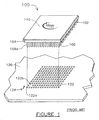
- FIG. 1 shows a generic, packaged integrated circuit 100, and is intended to be representative of any conventional package. This Figure is included to show some of numerous ways that others have provided features on integrated circuit packages and printed circuit boards, and is not intended in any way to be a limiting representation of the prior art.
- an IC device is tested briefly while still on the wafer. ICs failing the tests are discarded. ICs passing the tests are packaged, then marked with product tracking information.
- the package is marked on the front with additional information intended for the customer, typically product identity information.
- Product tracking information may also be included intended for the manufacturer.
- a marked IC may display the company name and logo, an alphanumeric string including the product identity information (PRODUCTIDENTITY), and one or more strings including the product tracking information (PRODUCTTRACKING).
- FIG. 1 shows the marked information in more detail.
- the IC of FIG. 1 displays the product identity information in the form of a product designator (Prod), package identifier (pkg), and speed grade (spd-grade).
- Product tracking information includes the wafer lot, processing date, assembly lot, and assembly date.
- the package body 102 of the integrated circuit 100 shown in FIG.1 has four corners, one of which 104 is chamfered to indicate a particular orientation of the package (e.g., the location of pin number 1).
- the package body has a top surface 110, and a bottom surface opposite the top surface.
- a plurality of pins 106 extend from the bottom surface of the package body in a rectangularly shaped array, and are electrically connected to a semiconductor (integrated) circuit die (not shown) contained within the package body 102.
- the integrated circuit 100 may be mounted to a printed circuit board (PCB) 120 having a plurality of holes 122 for receiving the plurality of pins 106, and the pins and holes may be arranged in symmetrical arrays or about the periphery of the package.
- PCB printed circuit board
- the device 100 could be inserted in any of four orientations into the PCB 120--only one of which orientation is correct.
- the chamfered corner 104 indicates a particular orientation, and the printed circuit board may be provided with a mark 124 ("1"), or the like, indicating the location of a particular hole 122a corresponding to pin #1 which can be established to be the pin 106a nearest to the chamfered edge 104 of the package 102.
- an integrated circuit package having at least a product identity information and a product tracking information, said integrated circuit package comprising:
- the product tracking information is encoded having the form of a bar code.
- the encoded product tracking information has the form of a nxm matrix or a nxn matrix whereby n and m are integers.
- this encoded product tracking information is located on the surface indicating the location of a reference pin or a reference side or a reference corner.
- the encoded product tracking information is provided in a colour, other than white or black, that is either applied as a coating or a label to the top surface of the device or incorporated into the material forming the body of the device package. Typically this is done by inking and curing.
- the encoded product information is applied by a laser to the top surface of the device or incorporated into the material forming the body of the device package.
- a laser is much less likely to damage an IC than other known marking methods. Further, the laser process is much faster than the inking and curing.
- the encoded product tracking information is applied to (or incorporated into) a particular surface of the packaged semiconductor device, but must not completely cover the package.
- the encoded product tracking information is applied to (or incorporated into) at least one selected area of the top surface of the device.
- the at least one selected area encompasses less than 75% of a visible surface of the device, including less than 50%, less than 25%, less than 20%, less than 15%, less than 10%, and less than 5%.
- FIG. 3A is a top view of an integrated circuit package 300a having leads (electrical connections) shown as peripheral leads (such as gull wing or J-type leads) 302a, 302b, 302c, and 302d disposed along respective sides 312a, 312b, 312c, and 312d of the integrated circuit package 300a.
- leads electrical connections
- peripheral leads such as gull wing or J-type leads
- a colored inked 16x16 data code matrix 320a appears on a surface 314 of the integrated circuit package 300a.
- the inked data code matrix 320a occupies an area substantially less than the total area of the surface 314 (e.g., less than 75% of the area of the surface 314), and is positioned towards a reference corner 310a (between sides 312a and 312b) of the integrated circuit package 300a. To an observer, this positioning of the inked data code matrix 320a can be used to visually indicate that the corner 310a is a reference corner.
- pin (ball) #1 could be the pin at the corner of the pin (ball) array under the corner 310a.
- FIG. 3B is a top view of an integrated circuit package 300b, similar to 300a (FIG. 3A), but with different markings. Like the integrated circuit package 300a, the integrated circuit package 300b has leads 302a', 302b', 302c', and 302d' disposed along respective sides of the package 300b.
- a lasermarked data code matrix 320b bearing the product tracking information appears on a surface 314' of the package 300b.
- the lasermarked data code matrix 320b has an area less than 25% of the total area of the surface 314', but is significantly larger than characters in a printed text marking 342 on the surface 314', and such lasermarked data code matrix 320b is readily discerned from distances well beyond reading distance.
- the lasermarked data code matrix 320b is preferably positioned on the surface 314' towards a reference corner 310b of the package (in a manner similar to the offset orientation of the inked data code matrix in FIG. 3a).
- a logo 340 appears on the surface 314'.
- the logo 340 includes the characters "LOGIC” which are not necessarily the color(s) of the "INFINEON” characters.
- the "LOGIC” characters could be black or white shades surrounded by the colored square portion--providing a complex internal shaded region to the lasermarked data code matrix 320b enhancing the contrast.
- the data code matrix bearing the product tracking information can be used to convey additional information about one or more characteristics of the integrated circuit.
Abstract
An integrated circuit package (300b) having at least a product
identity information and a product tracking information (340), said
integrated circuit package comprising:

Description
- The invention relates to packaged integrated circuits (ICs). More particularly, the invention relates integrated circuit packages with marked product tracking information.
- ICs are normally "packaged" prior to sale, e.g., mounted in plastic or ceramic carriers that protect the IC. The IC package is then typically mounted on a circuit board, while "package pins" incorporated in the package allow electrical contact (through fragile internal "bond wires") between the pads of the IC and traces on the board. Commonly used packages include dual in-line (DIP) packages, ball grid arrays (BGA), and many other well-known packages.
- Because many different ICs are generally available in a given package, packaged ICs are normally marked with both product tracking information and product identity information prior to sale.
- The product tracking information typically includes the wafer fabrication lot number and the date on which the wafer was fabricated, as well as the assembly lot number and the date on which the packaged IC was assembled. This information allows the manufacturer to track the manufacturing process and assists in solving manufacturing problems. Basic principles about these informations and methods of marking these informations are disclosed e.g. in the US 5,644,102 and US 6,359,248.
- Product identity information typically includes designations for the product type, package type, and performance (speed grade) of the IC.
- Among the various characteristics of integrated circuit devices which can be marked additionally are:
- testing level (e.g., commercial, industrial, mil-spec);
- radiation hardness of the integrated circuit;
- functionality (e.g., microprocessor, peripheral controller, memory device, etc.);
- source or origin of the device (e.g., manufacturer, distributor, etc.);
- temperature and/or humidity range for operation;
- method or process for design or manufacture (e.g., CMOS11, CMOS12 BiCMOS6HFC, etc.);
- device speed;
- testing level (e.g., commercial, industrial, mil-spec);
- availability of added (optional) functionality;
- location and function of groups of functionally related pins of the integrated circuit device;
- location of reference pin, side, corner, etc.
- FIG. 1 shows a generic, packaged integrated
circuit 100, and is intended to be representative of any conventional package. This Figure is included to show some of numerous ways that others have provided features on integrated circuit packages and printed circuit boards, and is not intended in any way to be a limiting representation of the prior art. - Typically, an IC device is tested briefly while still on the wafer. ICs failing the tests are discarded. ICs passing the tests are packaged, then marked with product tracking information.
- The package is marked on the front with additional information intended for the customer, typically product identity information. Product tracking information may also be included intended for the manufacturer.
- For example, a marked IC may display the company name and logo, an alphanumeric string including the product identity information (PRODUCTIDENTITY), and one or more strings including the product tracking information (PRODUCTTRACKING). FIG. 1 shows the marked information in more detail. The IC of FIG. 1 displays the product identity information in the form of a product designator (Prod), package identifier (pkg), and speed grade (spd-grade). Product tracking information includes the wafer lot, processing date, assembly lot, and assembly date.
- Due to the ongoing miniaturization and shrinking of the semiconductor devices it becomes very hard to provide all this information on one the top surface of the package since the available area is becoming smaller and smaller. Especially, providing the product tracking information by alphanummeric strings is becoming almost impossible.
- Therefore, it is known, to mark the product tracking information on the bottom of the package and the more important product identity information is marked on the front. This is shown in FIG. 2A and 2B. However, this method is very complicated and needs additional tools in the marking equipment.
- Furthermore, it is a disadvantage in having this information on the bottom since this information is not visible after mounting the IC on the printed circuit board.
- The
package body 102 of the integratedcircuit 100 shown in FIG.1 has four corners, one of which 104 is chamfered to indicate a particular orientation of the package (e.g., the location of pin number 1). The package body has atop surface 110, and a bottom surface opposite the top surface. A plurality ofpins 106 extend from the bottom surface of the package body in a rectangularly shaped array, and are electrically connected to a semiconductor (integrated) circuit die (not shown) contained within thepackage body 102. Theintegrated circuit 100 may be mounted to a printed circuit board (PCB) 120 having a plurality ofholes 122 for receiving the plurality ofpins 106, and the pins and holes may be arranged in symmetrical arrays or about the periphery of the package. - Evidently, in such a case, the
device 100 could be inserted in any of four orientations into thePCB 120--only one of which orientation is correct. To ensure that thedevice 100 is inserted into thePCB 120 in the proper orientation, thechamfered corner 104 indicates a particular orientation, and the printed circuit board may be provided with a mark 124 ("1"), or the like, indicating the location of aparticular hole 122a corresponding to pin #1 which can be established to be thepin 106a nearest to thechamfered edge 104 of thepackage 102. - In the assembly and subsequent inspection of semiconductor devices to circuit boards, it is essential that the proper device be mounted to the proper site on the board, and that the device is properly oriented at its location.
- For example, if the device is rotated 90, 180 or 270 degrees from its proper orientation it most certainly will not function as planned, since the pin-outs would be entirely wrong. To this end, certain semiconductor packages have some sort of locating/orienting feature, such as one of the corners of the package body being chamfered, an advertently missing pin, or the like. These solutions are complex, and require re-tooling to convert a non-orientation-sensitive package design to an orientation-sensitive package design.
- Therefore it is a problem applying indicia to a integrated circuit package that determines its "correct" orientation and simultanously providing the product identity information and product tracking information on top surfaces if there is only a small area available.
- According to the invention, this problem is solved by an integrated circuit package having at least a product identity information and a product tracking information, said integrated circuit package comprising:
- an integrated circuit device; and
- a package body (whether ceramic, plastic, epoxy, or the like) having a top surface and a bottom surface, the product tracking information being located on the top surface of the package body indicating a unique orientation of the integrated circuit device.
-
- In one embodiment the product tracking information is encoded having the form of a bar code. In a more preferred embodiment the encoded product tracking information has the form of a nxm matrix or a nxn matrix whereby n and m are integers.
- In a preferred embodiment this encoded product tracking information is located on the surface indicating the location of a reference pin or a reference side or a reference corner.
- In a further embodiment the encoded product tracking information is provided in a colour, other than white or black, that is either applied as a coating or a label to the top surface of the device or incorporated into the material forming the body of the device package. Typically this is done by inking and curing.
- In an alternative preferred embodiment the encoded product information is applied by a laser to the top surface of the device or incorporated into the material forming the body of the device package. A laser is much less likely to damage an IC than other known marking methods. Further, the laser process is much faster than the inking and curing.
- To this end, the encoded product tracking information is applied to (or incorporated into) a particular surface of the packaged semiconductor device, but must not completely cover the package.
- According to an aspect of the invention, the encoded product tracking information is applied to (or incorporated into) at least one selected area of the top surface of the device. For example, the at least one selected area encompasses less than 75% of a visible surface of the device, including less than 50%, less than 25%, less than 20%, less than 15%, less than 10%, and less than 5%.
- The present invention is illustrated by way of example, and not by way of limitation, in the following figures:
- FIG. 1 shows the perspective view of a packaged IC and indicates the information that may be marked on the package according to a first known method.
- FIGS. 2A and 2B show the bottom and top sides, respectively, of a packaged IC after marking with product tracking information according to a second known method.
- FIGS. 3A and 3B are top views of integrated circuit packages with marked product tracking information, according to the invention.
-
- FIG. 3A is a top view of an
integrated circuit package 300a having leads (electrical connections) shown as peripheral leads (such as gull wing or J-type leads) 302a, 302b, 302c, and 302d disposed alongrespective sides integrated circuit package 300a. - A colored inked 16x16
data code matrix 320a appears on asurface 314 of theintegrated circuit package 300a. The inkeddata code matrix 320a occupies an area substantially less than the total area of the surface 314 (e.g., less than 75% of the area of the surface 314), and is positioned towards areference corner 310a (betweensides integrated circuit package 300a. To an observer, this positioning of the inkeddata code matrix 320a can be used to visually indicate that thecorner 310a is a reference corner. In the case of a pin grid array (or ball grid array) type package, pin (ball) #1 could be the pin at the corner of the pin (ball) array under thecorner 310a. - FIG. 3B is a top view of an
integrated circuit package 300b, similar to 300a (FIG. 3A), but with different markings. Like theintegrated circuit package 300a, theintegrated circuit package 300b hasleads 302a', 302b', 302c', and 302d' disposed along respective sides of thepackage 300b. - A lasermarked
data code matrix 320b bearing the product tracking information appears on a surface 314' of thepackage 300b. The lasermarkeddata code matrix 320b has an area less than 25% of the total area of the surface 314', but is significantly larger than characters in a printed text marking 342 on the surface 314', and such lasermarkeddata code matrix 320b is readily discerned from distances well beyond reading distance. - The lasermarked
data code matrix 320b is preferably positioned on the surface 314' towards areference corner 310b of the package (in a manner similar to the offset orientation of the inked data code matrix in FIG. 3a). In addition to the lasermarkeddata code matrix 320b and printedtext markings 342, alogo 340 appears on the surface 314'. Thelogo 340 includes the characters "LOGIC" which are not necessarily the color(s) of the "INFINEON" characters. Thus, the "LOGIC" characters could be black or white shades surrounded by the colored square portion--providing a complex internal shaded region to the lasermarkeddata code matrix 320b enhancing the contrast. - It will be readily appreciated by one of ordinary skill in the art that the data code matrix bearing the product tracking information can be used to convey additional information about one or more characteristics of the integrated circuit.
- Among these various informations which can be added additionally to the product tracking information in form of a data code matrix are:
- testing level (e.g., commercial, industrial, mil-spec);
- radiation hardness of the integrated circuit;
- functionality (e.g., microprocessor, peripheral controller, memory device, etc.);
- source or origin of the device (e.g., manufacturer, distributor, subcontractor etc.);
- temperature and/or humidity range for operation;
- method or process for design or manufacture;
- device speed;
Claims (11)
- Integrated circuit package having at least a product identity information and a product tracking information, said integrated circuit package comprising:an integrated circuit device; anda package body having a top surface and a bottom surface, the product tracking information being located on the top surface of the package body indicating a unique orientation of the integrated circuit device.
- Integrated circuit package of claim 1, wherein the product tracking information is located on the top surface of the package body indicating a reference pin of the integrated circuit device.
- Integrated circuit package of claim 1, wherein the product tracking information is located on the top surface of the package body indicating a reference side of the integrated circuit device.
- Integrated circuit package of claim 1, wherein the product tracking information is located on the top surface of the package body indicating a reference corner of the integrated circuit device.
- Integrated circuit package of claim 1, wherein the product tracking information is encoded.
- Integrated circuit package of claim 5, wherein the product tracking information is provided as a bar code.
- Integrated circuit package of claim 5, wherein the product tracking information is provided as a matrix.
- Integrated circuit package of claim 1, wherein the product tracking information is applied as acoating or label to the top surface.
- Integrated circuit package of claim 1, wherein the product tracking information is incorporated into the material forming the package body.
- Integrated circuit package of claim 1, wherein the product tracking information is inked and cured on the top surface.
- Integrated circuit package of claim 1, wherein the product tracking information is applied on the top surface by a laser.
Priority Applications (2)
| Application Number | Priority Date | Filing Date | Title |
|---|---|---|---|
| EP03009828A EP1478022A1 (en) | 2003-05-13 | 2003-05-13 | Integrated circuit package marked with product tracking information |
| US10/843,814 US20040257230A1 (en) | 2003-05-13 | 2004-05-12 | Integrated circuit packages with marked product tracking information |
Applications Claiming Priority (1)
| Application Number | Priority Date | Filing Date | Title |
|---|---|---|---|
| EP03009828A EP1478022A1 (en) | 2003-05-13 | 2003-05-13 | Integrated circuit package marked with product tracking information |
Publications (1)
| Publication Number | Publication Date |
|---|---|
| EP1478022A1 true EP1478022A1 (en) | 2004-11-17 |
Family
ID=33016842
Family Applications (1)
| Application Number | Title | Priority Date | Filing Date |
|---|---|---|---|
| EP03009828A Ceased EP1478022A1 (en) | 2003-05-13 | 2003-05-13 | Integrated circuit package marked with product tracking information |
Country Status (2)
| Country | Link |
|---|---|
| US (1) | US20040257230A1 (en) |
| EP (1) | EP1478022A1 (en) |
Cited By (3)
| Publication number | Priority date | Publication date | Assignee | Title |
|---|---|---|---|---|
| EP2625708A1 (en) * | 2010-10-04 | 2013-08-14 | SanDisk Semiconductor (Shanghai) Co., Ltd. | Discrete component backward traceability and semiconductor device forward traceability |
| US8754538B2 (en) | 2008-06-24 | 2014-06-17 | Infineon Technologies Ag | Semiconductor chip including identifying marks |
| EP4270476A1 (en) | 2022-04-29 | 2023-11-01 | Infineon Technologies Austria AG | Semiconductor package and method for marking a semiconductor package |
Families Citing this family (1)
| Publication number | Priority date | Publication date | Assignee | Title |
|---|---|---|---|---|
| US8689434B2 (en) * | 2009-10-14 | 2014-04-08 | Nanya Technology Corporation | Integrated circuit manufacturing system |
Citations (4)
| Publication number | Priority date | Publication date | Assignee | Title |
|---|---|---|---|---|
| JPS59175751A (en) * | 1983-03-26 | 1984-10-04 | Mitsubishi Electric Corp | Resin seal type semiconductor device |
| US5644102A (en) * | 1994-03-01 | 1997-07-01 | Lsi Logic Corporation | Integrated circuit packages with distinctive coloration |
| US20020036235A1 (en) * | 1997-06-27 | 2002-03-28 | Isao Kudo | Semiconductor device and an information management system thereof |
| US20020167076A1 (en) * | 2001-04-13 | 2002-11-14 | Kenichi Shirasaka | Semiconductor package and semiconductor package mounting method |
Family Cites Families (2)
| Publication number | Priority date | Publication date | Assignee | Title |
|---|---|---|---|---|
| US6359248B1 (en) * | 1999-08-02 | 2002-03-19 | Xilinx, Inc. | Method for marking packaged integrated circuits |
| US6352204B2 (en) * | 1999-08-04 | 2002-03-05 | Industrial Data Entry Automation Systems Incorporated | Optical symbol scanner with low angle illumination |
-
2003
- 2003-05-13 EP EP03009828A patent/EP1478022A1/en not_active Ceased
-
2004
- 2004-05-12 US US10/843,814 patent/US20040257230A1/en not_active Abandoned
Patent Citations (4)
| Publication number | Priority date | Publication date | Assignee | Title |
|---|---|---|---|---|
| JPS59175751A (en) * | 1983-03-26 | 1984-10-04 | Mitsubishi Electric Corp | Resin seal type semiconductor device |
| US5644102A (en) * | 1994-03-01 | 1997-07-01 | Lsi Logic Corporation | Integrated circuit packages with distinctive coloration |
| US20020036235A1 (en) * | 1997-06-27 | 2002-03-28 | Isao Kudo | Semiconductor device and an information management system thereof |
| US20020167076A1 (en) * | 2001-04-13 | 2002-11-14 | Kenichi Shirasaka | Semiconductor package and semiconductor package mounting method |
Non-Patent Citations (2)
| Title |
|---|
| AGAPAKIS J. ET AL: "Improving Yield, Productivity, and Quality in Test Assembly & Packaging Through Direct Part Marking and Unit Level Traceability", SEMI TECHNOLOGY SYMPOSIUM: INTERNATIONAL ELECTRONIC MANUFACTURING TECHNOLOGY (IEMT) SYMPOSIUM, 17 July 2002 (2002-07-17), NEW YORK, NY : IEEE, US, pages 154 - 158, XP010603409 * |
| PATENT ABSTRACTS OF JAPAN vol. 009, no. 031 (E - 295) 9 February 1985 (1985-02-09) * |
Cited By (6)
| Publication number | Priority date | Publication date | Assignee | Title |
|---|---|---|---|---|
| US8754538B2 (en) | 2008-06-24 | 2014-06-17 | Infineon Technologies Ag | Semiconductor chip including identifying marks |
| US9171806B2 (en) | 2008-06-24 | 2015-10-27 | Infineon Technologies Ag | Method of making a semiconductor chip including identifying marks |
| EP2625708A1 (en) * | 2010-10-04 | 2013-08-14 | SanDisk Semiconductor (Shanghai) Co., Ltd. | Discrete component backward traceability and semiconductor device forward traceability |
| EP2625708A4 (en) * | 2010-10-04 | 2014-10-08 | Sandisk Semiconductor Shanghai Co Ltd | Discrete component backward traceability and semiconductor device forward traceability |
| US10229886B2 (en) | 2010-10-04 | 2019-03-12 | Sandisk Semiconductor (Shanghai) Co. Ltd. | Discrete component backward traceability and semiconductor device forward traceability |
| EP4270476A1 (en) | 2022-04-29 | 2023-11-01 | Infineon Technologies Austria AG | Semiconductor package and method for marking a semiconductor package |
Also Published As
| Publication number | Publication date |
|---|---|
| US20040257230A1 (en) | 2004-12-23 |
Similar Documents
| Publication | Publication Date | Title |
|---|---|---|
| US5644102A (en) | Integrated circuit packages with distinctive coloration | |
| US7265454B2 (en) | Semiconductor device and method of producing high contrast identification mark | |
| USRE40623E1 (en) | Method and apparatus for identifying integrated circuits | |
| US6359248B1 (en) | Method for marking packaged integrated circuits | |
| KR101006777B1 (en) | A semiconductor devices with leds and a fabricating method thereof | |
| BRPI9911407B1 (en) | Radio Frequency Identification Tag, Antenna and Method for Manufacturing a Radio Frequency Identification Tag | |
| US20040190256A1 (en) | Heat sink with visible logo | |
| JP2005142186A (en) | Semiconductor device and its manufacturing method | |
| US20070114652A1 (en) | Surface-mount packaging for chip | |
| EP1478022A1 (en) | Integrated circuit package marked with product tracking information | |
| US9941218B2 (en) | Display apparatus capable of easily acquiring identification about a display panel and a driving chip | |
| US20090126979A1 (en) | Semiconductor package circuit board and method of forming the same | |
| US6777821B2 (en) | Ball grid array x-ray orientation mark | |
| JP4846299B2 (en) | Marking method for semiconductor device | |
| JPH05267482A (en) | Semiconductor device | |
| KR19980020175A (en) | A reel-type printed circuit board | |
| US20240032188A1 (en) | Substrate | |
| JPH1126895A (en) | Face mounted parts | |
| JPS61131549A (en) | Semiconductor circuit package | |
| WO2003073504A1 (en) | Semiconductor device and method of producing high contrast identification mark | |
| JP2000223802A (en) | Printed circuit board | |
| KR101824117B1 (en) | Ball grid array package having index marker and method for manufacturing the same | |
| JPH02299216A (en) | Semiconductor device | |
| US8377747B2 (en) | Interleaf for leadframe identification | |
| KR20090098066A (en) | Substrate for semiconductor pacakge and method of manufacturing semiconductor package using the same |
Legal Events
| Date | Code | Title | Description |
|---|---|---|---|
| PUAI | Public reference made under article 153(3) epc to a published international application that has entered the european phase |
Free format text: ORIGINAL CODE: 0009012 |
|
| AK | Designated contracting states |
Kind code of ref document: A1 Designated state(s): AT BE BG CH CY CZ DE DK EE ES FI FR GB GR HU IE IT LI LU MC NL PT RO SE SI SK TR |
|
| AX | Request for extension of the european patent |
Extension state: AL LT LV MK |
|
| 17P | Request for examination filed |
Effective date: 20050204 |
|
| 17Q | First examination report despatched |
Effective date: 20050225 |
|
| AKX | Designation fees paid |
Designated state(s): DE FR GB |
|
| STAA | Information on the status of an ep patent application or granted ep patent |
Free format text: STATUS: THE APPLICATION HAS BEEN REFUSED |
|
| 18R | Application refused |
Effective date: 20081030 |