EP1477849A2 - Methode zur Reproduktion eines dreidimensionalen Prägemusters in einem Empfangsmaterial unbestimmter Grösse - Google Patents
Methode zur Reproduktion eines dreidimensionalen Prägemusters in einem Empfangsmaterial unbestimmter Grösse Download PDFInfo
- Publication number
- EP1477849A2 EP1477849A2 EP03027335A EP03027335A EP1477849A2 EP 1477849 A2 EP1477849 A2 EP 1477849A2 EP 03027335 A EP03027335 A EP 03027335A EP 03027335 A EP03027335 A EP 03027335A EP 1477849 A2 EP1477849 A2 EP 1477849A2
- Authority
- EP
- European Patent Office
- Prior art keywords
- photopolymer
- layer
- shim
- silicone
- imprint
- Prior art date
- Legal status (The legal status is an assumption and is not a legal conclusion. Google has not performed a legal analysis and makes no representation as to the accuracy of the status listed.)
- Withdrawn
Links
Images







Classifications
-
- G—PHYSICS
- G03—PHOTOGRAPHY; CINEMATOGRAPHY; ANALOGOUS TECHNIQUES USING WAVES OTHER THAN OPTICAL WAVES; ELECTROGRAPHY; HOLOGRAPHY
- G03F—PHOTOMECHANICAL PRODUCTION OF TEXTURED OR PATTERNED SURFACES, e.g. FOR PRINTING, FOR PROCESSING OF SEMICONDUCTOR DEVICES; MATERIALS THEREFOR; ORIGINALS THEREFOR; APPARATUS SPECIALLY ADAPTED THEREFOR
- G03F7/00—Photomechanical, e.g. photolithographic, production of textured or patterned surfaces, e.g. printing surfaces; Materials therefor, e.g. comprising photoresists; Apparatus specially adapted therefor
- G03F7/20—Exposure; Apparatus therefor
-
- B—PERFORMING OPERATIONS; TRANSPORTING
- B81—MICROSTRUCTURAL TECHNOLOGY
- B81C—PROCESSES OR APPARATUS SPECIALLY ADAPTED FOR THE MANUFACTURE OR TREATMENT OF MICROSTRUCTURAL DEVICES OR SYSTEMS
- B81C99/00—Subject matter not provided for in other groups of this subclass
- B81C99/0075—Manufacture of substrate-free structures
- B81C99/009—Manufacturing the stamps or the moulds
-
- B—PERFORMING OPERATIONS; TRANSPORTING
- B82—NANOTECHNOLOGY
- B82Y—SPECIFIC USES OR APPLICATIONS OF NANOSTRUCTURES; MEASUREMENT OR ANALYSIS OF NANOSTRUCTURES; MANUFACTURE OR TREATMENT OF NANOSTRUCTURES
- B82Y10/00—Nanotechnology for information processing, storage or transmission, e.g. quantum computing or single electron logic
-
- B—PERFORMING OPERATIONS; TRANSPORTING
- B82—NANOTECHNOLOGY
- B82Y—SPECIFIC USES OR APPLICATIONS OF NANOSTRUCTURES; MEASUREMENT OR ANALYSIS OF NANOSTRUCTURES; MANUFACTURE OR TREATMENT OF NANOSTRUCTURES
- B82Y40/00—Manufacture or treatment of nanostructures
-
- G—PHYSICS
- G03—PHOTOGRAPHY; CINEMATOGRAPHY; ANALOGOUS TECHNIQUES USING WAVES OTHER THAN OPTICAL WAVES; ELECTROGRAPHY; HOLOGRAPHY
- G03F—PHOTOMECHANICAL PRODUCTION OF TEXTURED OR PATTERNED SURFACES, e.g. FOR PRINTING, FOR PROCESSING OF SEMICONDUCTOR DEVICES; MATERIALS THEREFOR; ORIGINALS THEREFOR; APPARATUS SPECIALLY ADAPTED THEREFOR
- G03F7/00—Photomechanical, e.g. photolithographic, production of textured or patterned surfaces, e.g. printing surfaces; Materials therefor, e.g. comprising photoresists; Apparatus specially adapted therefor
- G03F7/0002—Lithographic processes using patterning methods other than those involving the exposure to radiation, e.g. by stamping
-
- G—PHYSICS
- G03—PHOTOGRAPHY; CINEMATOGRAPHY; ANALOGOUS TECHNIQUES USING WAVES OTHER THAN OPTICAL WAVES; ELECTROGRAPHY; HOLOGRAPHY
- G03F—PHOTOMECHANICAL PRODUCTION OF TEXTURED OR PATTERNED SURFACES, e.g. FOR PRINTING, FOR PROCESSING OF SEMICONDUCTOR DEVICES; MATERIALS THEREFOR; ORIGINALS THEREFOR; APPARATUS SPECIALLY ADAPTED THEREFOR
- G03F7/00—Photomechanical, e.g. photolithographic, production of textured or patterned surfaces, e.g. printing surfaces; Materials therefor, e.g. comprising photoresists; Apparatus specially adapted therefor
- G03F7/0015—Production of aperture devices, microporous systems or stamps
Definitions
- the present invention relates generally to a method for replicating a three-dimensional imprint pattern on a compliant media of arbitrary size. More specifically, the present invention relates to a method for replicating one or more photopolymer shims that include an imprint stamp on a compliant media that can be used to transfer a high resolution three-dimensional imprint pattern carried on the imprint stamp to another media that is brought into contact with the compliant media in a soft lithography printing process.
- shims are often created from smaller masters using a process called recombination.
- a small master stamp is alternately heated and cooled while embossing a thermoplastic substrate.
- a pattern in the master stamp is transferred to the thermoplastic substrate.
- the thermoplastic substrate can then be plated or otherwise coated to create other shims.
- the machines used for the aforementioned process are expensive (e.g. ⁇ $90,000) and are not guaranteed to work with patterns that are submicron (i.e. less than 1.0 ⁇ m) in dimension due to a relatively high viscosity of the thermoplastic substrate when in a molten state.
- Other proprietary processes are available, such as automated holographic systems, for example. However, those proprietary systems are also expensive and the cost per shim can exceed several thousand dollars per shim.
- PDMS Polydimethyl Siloxane
- the present invention is embodied in a method for replicating a high resolution three-dimensional imprint pattern on a compliant media of arbitrary size.
- the compliant media can be connected with a flexible belt material or it can be connected with a cylinder.
- the compliant media carries an imprint stamp that can include features having a submicron (i.e. less than 1.0 ⁇ m) feature size.
- the compliant media can be made any size and the imprint patterns carried by the compliant media can be made from the same master substrate or from different master substrates.
- the compliant media of the present invention include it can be manufactured at a low cost in a bench top laboratory environment, the compliant media is durable, flexible, and can be made from optically transparent materials, particularly, materials that are optically transparent to ultraviolet light.
- the compliant media can be connected with an optically transparent belt or cylinder for use in a soft lithography process wherein the imprint stamp carried by the compliant media is used to emboss another substrate that can be coated with a photopolymer material and is then cured by an ultraviolet light source contemporaneously with the embossing step.
- the present invention is embodied in a method for fabricating a high resolution three-dimensional imprint pattern on a compliant media of arbitrary size.
- the compliant media can be connected with another substrate such as a cylinder or a belt.
- the belt can be a flexible belt.
- the imprint pattern can be used as part of a lithographic print process, wherein, another coated substrate is passed under the belt or cylinder and the imprint pattern on the compliant media is embossed (i.e. transferred) to the coated substrate.
- the coated substrate can be coated with a material such as a photopolymer and the photopolymer can be cured contemporaneously with the embossing in order to fix the imprinted pattern in the photopolymer.
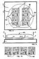
- a master substrate 11 is patterned and then etched to form an imprint pattern 20 therein.
- the master substrate 11 is coated with a material 155 that will serve as an etch mask.
- the material 155 can be a photoresist material that is commonly used in the microelectronics art.
- a mask 151 that carries a pattern 153 to be formed in the master substrate 11 is illuminated with light 154 which exposes the material 155 with the pattern 153.
- the material 155 is developed to remove those portions of the material 155 that were exposed to the light 154.
- the master substrate 11 is etched with an etch material to remove those portions of the master substrate 11 that are not covered with the material 155 .
- a plurality of imprint patterns 20p are formed in the master substrate 11 .
- the imprint patterns 20p define an imprint stamp 20 on the master substrate 11 .
- the imprint stamp 20 can include imprint patterns 20p that vary in all three dimensions of width, length, and height. In the cross-sectional view of FIG. 4 and the top plan view of FIG. 5 , the imprint patterns 20p vary in a width dimension do, a height dimension h 0 , and a length dimension L 0 .
- the actual dimensions of the imprint patterns 20p will be application dependent and will depend to a large extent on the lithography process used for the patterning the material 155 . For example, if a state-of-the-art microelectronics lithography process is used, then the dimensions ( d 0 , h 0 , L 0 ) can be of a sub-micrometer scale, that is, less than 1.0 ⁇ m.
- the imprint patterns 20p can be nano-imprint patterns that can have dimensions ( d 0 , h 0 , L 0 ) of 100.0 nm or less. Accordingly, the imprint stamp 20 would be a nano-imprint stamp with imprint patterns 20p that have nanometer-size dimensions ( d 0 , h 0 , L 0 ).
- Lithography processes that are well understood in the microelectronics art can be used to pattern and etch the master substrate 11 .
- a photolithography process using a photoresist for the material 155 and an etch process such as reactive ion etching (RIE) can be used to form the imprint stamp 20 in the master substrate 11 .
- RIE reactive ion etching
- Suitable materials for the master substrate 11 include but are not limited to a silicon (Si) substrate and a silicon (Si) wafer.
- the master substrate 11 is a silicon wafer with a wafer flat 11F .
- Four of the imprint stamps 20 are formed in the master substrate 11 .
- the silicon wafer can be any size. For example a 4.0 inch silicon wafer was used as the master substrate 11 for four of the imprint stamps 20 . Larger diameter silicon wafers (e.g. 8 inch or 12 inch) can be used to provide a larger surface area for more of the imprint stamps 20 or for larger imprint stamps 20 .
- the imprint patterns 20p appear to be identical in FIG. 5
- the imprint stamps 20 can include imprint patterns 20p that vary (i.e are not identical) among the imprint stamps 20 .
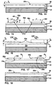
- a release layer 13 is deposited over the imprint patterns 20p .
- the release layer 13 includes a first thickness t 1 that is operative to conformally coat the imprint patterns 20p such that the first thickness t 1 is substantially equally thick on the vertical and the horizontal surfaces of the imprint patterns 20p .
- Suitable materials for the release layer 13 include but are not limited to a fluorocarbon material.
- the fluorocarbon material for the release layer 13 can be deposited using a plasma deposition of a trifluoromethane (CHF 3 ) gas for about 5.0 minutes.
- the first thickness t 1 will be application dependent; however, as will be discussed below, the release layer 13 is operative to provide a non-stick surface upon which to apply a silicone-based elastomer material that will later be released from the release layer 13 . Therefore, the release layer 13 can be a very thin layer having a first thickness t 1 that is from about 50.0 nm to about 150.0 nm thick.
- a silicone-based elastomer layer 15 is deposited over the release layer 13 to a first depth d 1 that completely covers the imprint patterns 20p .
- the master substrate 11 should be substantially level. This can be accomplished by placing the master substrate 11 on a level surface or a level vacuum chuck prior to depositing the silicone-based elastomer layer 15 , for example.
- the silicone-based elastomer layer 15 is then cured by heating H the master substrate 11 .
- the curing can be accomplished by baking the master substrate 11 at a predetermined temperature for a predetermined amount of time.
- the actual time and temperature will be application dependent and will also depend on the type of material used for the silicone-based elastomer layer 15 .
- Suitable materials for the silicone-based elastomer layer 15 include but are not limited to Polydimethyl Siloxane (PDMS ), DOW CORNING® silicone-based conformal coatings including SYLGARD® 182 silicone elastomer, SYLGARD® 183 silicone elastomer, SYLGARD® 184 silicone elastomer, and SYLGARD® 186 silicone elastomer.
- the first depth d 1 of the silicone-based elastomer layer 15 can be application dependent. However, in a preferred embodiment, the first depth d 1 of the silicone-based elastomer layer 15 is from about 0.5 mm to about 1.5 mm.
- the curing of the silicone-based elastomer layer 15 can be accomplished by baking the master substrate 11 in an oven or the like. The predetermined temperature and the predetermined amount of time for the curing can be for about 4.0 hours at a temperature of about 100.0 °C.
- a cover layer 16 having a second thickness t 2 is applied over the already deposited silicone-based elastomer layer 15.
- the cover layer 16 is a Polyester film and the second thickness t 2 is from about 50.0 ⁇ m to about 150.0 ⁇ m.
- the cover layer 16 may be used to planarize any surface anomalies in the silicone-based elastomer layer 15 that cause deviations from a substantially planar surface 15s of the silicone-based elastomer layer 15 .
- a complementary image of the imprint patterns 20p are replicated 20r in the silicone-based elastomer layer 15 such that an imprint stamp 20a is formed in the silicone-based elastomer layer 15 (see FIGS. 8 through 10 ).
- the silicone-based elastomer layer 15 is released from the release layer 13 .
- a tip of a pair of tweezers or an edge of a knife or razor, such as an X-Acto® Knife, can be used to separate the silicone-based elastomer layer 15 from the release layer 13 as depicted by a knife edge K and a dashed arrow inserted between the silicone-based elastomer layer 15 and the release layer 13 .
- the silicone-based elastomer layer 15 can then be lifted off of the release layer 13 by grabbing an edge of the silicone-based elastomer layer 15 and peeling off (see dashed arrow P ) the silicone-based elastomer layer 15 from the release layer 13 . If the above mentioned cover layer 16 is used, then the cover layer 16 is removed from the silicone-based elastomer layer 15 before the silicone-based elastomer layer 15 is released from the release layer 13 .
- the imprint stamp 20a is removed from an excess portion of the silicone-based elastomer layer 15 that surrounds the imprint stamp 20a. If the above mentioned cover layer 16 is used, then the imprint stamp 20a is removed from an excess portion of the silicone-based elastomer layer 15 and the cover layer 16 that surround the imprint stamp 20a .
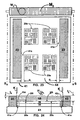
- the imprint stamp 20a can be removed from the excess portion by placing the silicone-based elastomer layer 15 on a substantially flat substrate 21 and then cutting C around a perimeter (see dashed lines in FIGS. 8 and 9 ) of the imprint stamp 20a to release the excess portions of the silicone-based elastomer layer 15 or the silicone-based elastomer layer 15 and the cover layer 16 from the imprint stamp 20a .
- a knife, razor, die, or the like can be used to accomplish the cutting as depicted by a knife K in FIG. 9 .
- the substantially flat substrate 21 can be a material including but not limited to a glass, a metal, a plastic, and quartz.
- the substantially flat substrate 21 can be a glass plate.
- the above mentioned steps may be repeated as necessary to produce additional imprint stamps 20a using the master substrate 11 .
- One advantage of the present invention is that the master substrate 11 is not damaged by the aforementioned process steps. Consequently, the same master substrate 11 can be repeatedly used to produce several imprint stamps 20a . Therefore, the cost of patterning and etching the master substrate 11 and depositing the release layer 13 can be amortized over several imprint stamps 20a.
- Another advantage of the present invention is that the master substrate 11 need not be cleaned after each use in order to remove contaminants, such as dust particles, because the silicone-based elastomer layer 15 flows around the particles and entrains them. Consequently, the master substrate 11 is self-cleaning because the particles are removed with the silicone-based elastomer layer 15 .
- a flat and thin plastic film 33 having a third thickness t 3 is placed on a flat and compliant silicone rubber backing 31 having a fourth thickness t 4 .
- Suitable materials for the thin plastic film 33 include but are not limited to a Polymide and a Polyester ( PET , Polyethylene Terephthalate).
- the third thickness t 3 and the fourth thickness t 4 will be application dependent.
- the third thickness t 3 of the thin plastic film 33 is from about 40.0 ⁇ m to about 100.0 ⁇ m and the fourth thickness t 4 of the silicone rubber backing 31 is from about 0.125 inches to about 0.25 inches.
- the fourth thickness t 4 of the silicone rubber backing 31 should be selected to ensure the silicone rubber backing 31 is complaint (i.e. not stiff).
- a surface 33s of the thin plastic film 33 is coated with a photopolymer solution 35 .
- the photopolymer solution 35 can include but is not limited to a mixture of about 50% of a photopolymer material and about 50% acetone. As will be describe below, the acetone will evaporate leaving a substantially photopolymer layer on the surface 33s of the thin plastic film 33 .
- the photopolymer material can include but is not limited to a Norland TM Optical Adhesive that cures when exposed to ultraviolet light. Preferably, the photopolymer material will cure in a time from about 5.0 seconds to about 60.0 seconds. For example, a Norland® NOA 83H photopolymer can be used for the photopolymer solution 35 .
- the photopolymer solution 35 is spread over the surface 33s of the thin plastic film 33 to form a photopolymer layer 35 having a fifth thickness t 5 .
- the spreading of the photopolymer solution 35 is accomplished using a Mayer bar M 1 that is wound with a wire W 1 having a first diameter.
- the Mayer bar M 1 slides S over the surface 33s and meters the photopolymer solution 35 so that the photopolymer layer 35 having a fifth thickness t 5 is formed.
- Any acetone in the photopolymer solution 35 substantially evaporates during the spreading process.
- the photopolymer layer 35 comprises substantially a photopolymer material as described above.
- the fifth thickness t 5 of the photopolymer layer 35 is from about 5.0 ⁇ m to about 10.0 ⁇ m.
- the first diameter of the wire W 1 will be application dependent.
- the first diameter of the wire W 1 is from about 50.0 ⁇ m micrometers to about 100.0 ⁇ m.
- a patterned surface 21a of the imprint stamp 20a is placed on the photopolymer layer 35 .
- Placing the imprint stamp 20a on the photopolymer layer 35 can include placing an edge e1 of the imprint stamp 20a in contact with the photopolymer layer 35 and holding the edge e1 down while progressively lowering ( see arrows L1 and d ) a remainder of the patterned surface 21a into contact with the photopolymer layer 35 .
- a pair of tweezers or a suction wand can be used to grasp an edge e2 to accomplish the lowering and to hold the edge e1 down.
- a rubber roller or the like can be used in conjunction with the progressive lowering to bring the patterned surface 21 a into contact with the photopolymer layer 35 .
- One advantage to the progressive lowering is that air entrapped between the photopolymer layer 35 and the patterned surface 20r is displaced so that air bubbles that can cause defects are not trapped between the photopolymer layer 35 and the patterned surface 20r .
- the imprint stamp 20a can be floated (see dashed arrow F ) over a surface 35s of the photopolymer layer 35 to position the imprint stamp 20a at a predetermined location on the photopolymer layer 35 .
- the floating F can be done manually using a tweezer or suction wand, or the floating F can be automated and a precision mechanical device, such as a robotic end effector, can be used to precisely position the imprint stamp 20a.
- the photopolymer layer 35 is cured to fix a position of the imprint stamp 20a on the photopolymer layer 35 and to transfer an image of the imprint pattern 20r to the photopolymer layer 35 .
- the photopolymer layer 35 is cured by irradiating the photopolymer layer 35 with an ultraviolet light UV of a predetermined intensity for a first time period.
- the photopolymer layer 35 hardens as it cures and an the image of the imprint pattern 20r that is transferred into the photopolymer layer 35 also hardens and is fixed in the photopolymer layer 35 as an imprint pattern 20s .
- the ultraviolet light UV can have a wavelength that includes but is not limited a range from about 300 nm to about 400 nm.
- the predetermined intensity of the ultraviolet light UV can include but is not limited to an intensity of about 150 mW/cm 2 .
- the first time period can include but is not limited to a time period from about 5.0 seconds to about 60.0 seconds.
- the ultraviolet light UV can be from a UVA ultraviolet light source.
- the imprint stamps 20a that are used to pattern the photopolymer layer 35 can have a thickness (see t A and t B in FIG. 16 ) that can vary and those variations in thickness will not effect the accuracy of the transfer of the imprint pattern 20r to imprint pattern 20s of the photopolymer layer 35 .
- the variations in thickness (t A and t B ) can be due to variations in the process used to make the imprint stamps 20a, variations in the first depth d 1 of FIG. 7 , or the use of different master substrates 11 to make different imprint stamps 20 with different imprint patterns 20p .
- the imprint stamps 20a are removed P from the photopolymer layer 35 so that the image of the imprint pattern 20r defines a photopolymer shim 36 with the imprint pattern 20s fixed therein.
- the imprint stamps 20a can be removed P using a pair of tweezers or the like to grab an edge (e1 or e2 ) and then lift the imprint stamps 20a from the photopolymer layer 35 (see dashed arrow P ).
- the photopolymer shim 36 is post-cured by heating the photopolymer shim 36 .
- the post-curing of the photopolymer shim 36 can include but is not limited to a time of about 1.0 hour at a temperature of about 100 °C.
- the photopolymer shim 36 can be rinsed with an acetone solution to remove chemical species which might inhibit curing of a silicone based elastomer material such as PDMS or the above mentioned SYLGARD® silicone-based elastomers.
- the post-curing of the photopolymer shim 36 drives off cure-inhibiting species and improves an adhesion of the photopolymer shim 36 to the thin plastic film 33 .
- a coating of a fluorocarbon material 37 having a sixth thickness t 6 is deposited on the photopolymer shim 36 .
- the sixth thickness t 6 can include but is not limited to a thickness from about 50.0 nm to about 150.0 nm.
- the fluorocarbon material 37 can be deposited using a plasma deposition of a trifluoromethane (CHF 3 ) gas for about 5.0 minutes.
- a tweezer or a knife edge can be inserted between the thin plastic film 33 and the silicone rubber backing 31 and the thin plastic film 33 can be pulled off of the silicone rubber backing 31 as shown by the dashed arrow P .
- the combination of the photopolymer shim 36 and the thin plastic film 33 will be referred to as the photopolymer shim 36 unless otherwise noted.
- the photopolymer shim 36 is attached to a support substrate 41 .
- the photopolymer shim 36 can be connected with the support substrate 41 by laying the photopolymer shim 36 on the support substrate 41 and fastening an end of the photopolymer shim 36 to the support substrate 41 using an adhesive.
- a high temperature adhesive tape T can be used.
- the support substrate 41 can be made from a material including but not limited to a glass and quartz.
- a shim stock 43 having a first height h 1 is attached to the support substrate 41 .
- the shim stock 43 can be connected with the support substrate 41 using an adhesive such as the above mentioned high temperature adhesive tape T , for example.
- the shim stock 43 is positioned adjacent to the photopolymer shim 36 and is spaced apart from the photopolymer shim 36 by a first distance D 1 so that there is a space between the shim stock 43 and the photopolymer shim 36 on a surface 41s of the support substrate 41 .
- the first height h 1 of the shim stock 43 should exceed a height h s of the photopolymer shim 36 as depicted in FIG. 22 .
- the first height h 1 and the first distance D 1 will be application dependent; however, the first height h 1 can be in a range including but not limited to from about 0.5 mm to about 1.5 mm and the first distance D 1 can be in a range including but not limited to from about 1.0 mm to about 2.0 mm.
- the shim stock 43 can be a material including but not limited to a metal, a glass, quartz, and stainless steel.
- the shim stock 43 can be a stainless steel shim stock and the first height h 1 can be about 0.5 mm.
- the support substrate 41 is preheated H to increase a temperature of the support substrate 41 in preparation for a coating of the shim stock 43 and the photopolymer shim 36 with a silicone-based elastomer material as will be discussed below.
- the silicone-based elastomer material is not coated on a cold or on a room temperature (i.e. from about 18.0 °C to about 28.0 °C) support substrate 41 .
- the preheated temperature for the support substrate 41 will be application dependent and the temperature should not exceed a temperature limit of the photopolymer shim 36 .
- the support substrate 41 can be preheated to a temperature of about 100 °C. A temperature of about 100 °C is below the temperature limits of most photopolymer materials.
- the photopolymer shim 36 and the shim stock 43 are coated with a compliant material 44 that completely covers the photopolymer shim 36 and the shim stock 43 (see FIG. 22 ).
- Suitable materials for the compliant material 44 include but are not limited to a silicone-based elastomer material and an amorphous fluoropolymer material.
- Suitable silicone-based elastomer materials include but are not limited to Polydimethyl Siloxane (PDMS ), DOW CORNING® silicone-based conformal coatings including SYLGARD® 182 silicone elastomer, SYLGARD® 183 silicone elastomer, SYLGARD® 184 silicone elastomer, and SYLGARD® 186 silicone elastomer.
- PDMS Polydimethyl Siloxane
- DOW CORNING® silicone-based conformal coatings including SYLGARD® 182 silicone elastomer, SYLGARD® 183 silicone elastomer, SYLGARD® 184 silicone elastomer, and SYLGARD® 186 silicone elastomer.
- the PDMS is a mixture of about 10.0 parts of a base and about 1.5 parts of a curing agent. The base and the curing agent can be mixed by weight or by volume as they have the same density.
- a suitable material for the amorphous fluoropolymer material includes but is not limited to TEFLON® AF .
- TEFLON® AF a DuPontTM TEFLON® AF has been used for the compliant material 44 .
- the compliant material 44 comprises the amorphous fluoropolymer material, the above mentioned preheating step of FIG. 21 is not required.
- the compliant material 44 is spread over the photopolymer shim 36 and the shim stock 43 to form a compliant media 45 that covers the photopolymer shim 36 and the shim stock 43 (see thicknesses t 8 and t 9 in FIG. 24 ).
- the imprint pattern 20s in the photopolymer shim 36 is transferred to the compliant media 45 so that an imprint stamp 20t is formed in the compliant media 45 .
- the spreading of the compliant material 44 is accomplished using a Mayer bar M 2 that is wound with a wire W 2 having a second diameter.
- the Mayer bar M 2 slides S over the shim stock 43 and meters the compliant material 44 to form a smooth and uniformly thick compliant media 45 .
- the compliant material 44 will cover the shim stock 43 by a thickness t 8 and will cover the photopolymer shim 36 by a thickness t 9 , where t 9 >> t 8 .
- the Mayer bar M 2 is wound with a much coarser diameter of wire than the Mayer bar M 1 that was discussed above.
- the second diameter of the wire W 2 will be application dependent.
- the second diameter of the wire W 2 is from about 1.0 mm to about 3.0 mm.
- a wire with a diameter of about 1.5 mm can be wound on the Mayer bar M 2 .
- the support substrate 41 is heated H .
- the surface 41s is operative to provide a surface for a portion 45c of the compliant media 45 to adhere to during and after the heating step.
- the time and temperature for the heating H of the substrate 41 will be application dependent, and as before, the temperature must not exceed a temperature limit for the photopolymer shim 36 or for the compliant media 45 .
- the support substrate 41 can be heated H for about 4.0 hours at a temperature of about 100.0 °C when the compliant media 45 is made from the silicone-based elastomer material. The heating H cures the silicone-based elastomer material.
- the support substrate 41 can be heated H for about 4.0 hours at a temperature of about 60.0 °C when the compliant media is made from the amorphous fluoropolymer material. In this case, the heating H drys out the amorphous fluoropolymer material.
- the support substrate 41 is cooled down.
- the support substrate 41 is allowed to cool down to a temperature of about a room temperature (i.e. from about 18.0 °C to about 28.0 °C).
- the shim stock 43 is removed from the support substrate 41 .
- the shim stock 43 can be removed by cutting K the compliant media 45 along an edge of the shim stock 43 that is adjacent to the photopolymer shim 36 .
- a knife, razor, or the like can be used to cut K the compliant media 45 .
- the shim stock 43 can be pulled off of the support substrate 41 .
- the edge of the shim stock 43 should be used as a guide for making the cut K because the portion 45c of the compliant media 45 adheres to the surface 41s of the support substrate 41 and the adhesion prevents the compliant media 45 from being prematurely separated from the substrate 41 .
- a first adhesive surface A 1 of a transfer adhesive layer 51 is applied to a surface 45s of the compliant media 45 so that the transfer adhesive layer 51 adheres to the compliant media 45 .
- the transfer adhesive layer 51 includes a seventh thickness t 7 and a second adhesive surface A 2 as will be described below.
- the first adhesive surface A 1 can be exposed, prior to being applied to the surface 45s , by peeling back P 1 a first backing 53 from the transfer adhesive layer 51 .
- the second adhesive surface A 2 can be exposed by peeling back P 2 a second backing 55 from the transfer adhesive layer 51 .
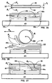
- the first adhesive surface A 1 can be connected with the surface 45s by using a roller 59 (see FIG. 26 ).
- the first adhesive surface A 1 is positioned at an edge of the compliant media 45 and then the roller 59 is rolled R across the second backing 55 to progressively apply the first adhesive surface A 1 across the surface 45s until the entire surface 45s is connected with the first adhesive surface A 1 (see FIG. 27 ).
- the roller 59 can be a rubber roller, for example. The roller 59 allows the first adhesive surface A 1 to be applied to the surface 45s without trapping air between the first adhesive surface A 1 and the surface 45s.
- the seventh thickness t 7 of the transfer adhesive layer 51 will be application dependent. However, because the transfer adhesive layer 51 will remain attached to the compliant media 45 and because it is desirable for the compliant media 45 to be flexible, the transfer adhesive layer 51 should be as thin as possible. Preferably, the seventh thickness t 7 of the transfer adhesive layer 51 is from about 20.0 ⁇ m thick to about 100.0 ⁇ m thick.
- the transfer adhesive layer 51 is an optically transparent material so that another photopolymer material that is brought into contact with the compliant media 45 and the imprint stamp 20t can be cured by a light source that is incident on both the transfer adhesive layer 51 and the compliant media 45 as will be described below.
- a suitable optically transparent material for the transfer adhesive layer 51 includes but is not limited to an Adhesives Research , Inc. TM ARclearTM DEV-8932 optically clear silicone adhesive.
- TM ARclearTM DEV-8932 optically clear silicone adhesive.
- the compliant media 45 can be separated from the support substrate 41 by using a knife, razor, suction wand, tweezer, or the like to initiate the separation of the compliant media 45 from the support substrate 41 as depicted by the knife K .
- the imprint stamp 20t includes a plurality of patterns 20q formed in the photopolymer shim 36 that complement the patterns 20p on the master substrate 11 (see FIGS. 5 and 6 ).
- the compliant media 45 is still connected with the photopolymer shim 36 and the thin plastic film 33 .
- An additional advantage of the present invention is that the photopolymer shim 36 and the thin plastic film 33 layer protect the imprint stamp 20t from damage during subsequent processing and handling steps that will be described below in reference to FIGS. 31 through 37b . Those processing and handling steps can be completed and then the photopolymer shim 36 and the thin plastic film 33 layers can be peeled off to expose the imprint stamp 20t .
- the combination of the layers comprising the photopolymer shim 36 and the thin plastic film 33 will be denoted as the photopolymer shim 36 (see FIG. 30 ).
- the combination of the compliant media 45 and the transfer adhesive layer 51 will be denoted as a compliant media 70 .
- the combination of the compliant media 70 and the photopolymer shim 36 will be denoted as a compliant assembly 75 .
- the compliant assembly 75 will be connected with a cylinder and a flexible belt material.
- FIGS. 31a, 31b , and 31c an L-shaped jig 73 that includes a horizontal section 73h and a vertical section 73v that forms a low vertical wall.
- the horizontal and vertical sections ( 73h, 73v ) are at a right angle ⁇ to each other.
- the sections ( 73h, 73v ) should be smooth and substantially flat.
- the L-shaped jig 73 can be used to effectuate a laminating of the compliant assembly 75 to a surface 69s of a cylinder 69 .
- the support substrate 41 can be placed on the horizontal section 73h and abutted against the vertical section 73v.
- a bed made from a smooth and flat piece of silicone rubber (not shown) can placed on the horizontal section 73h and an end of the bed is abutted against the vertical section 73v.
- the compliant assembly 75 is placed on top of the bed and is aligned with the vertical section 73v by using the vertical section 73v as a vertical straight edge. If the second backing 55 is still on the transfer adhesive layer 51, then the second backing 55 can be peeled off P 2 to expose the second adhesive surface A 2 .
- a cylinder 69 having an outer surface 69s is aligned with the horizontal section 73h and the vertical section 73v so that the outer surface 69s is tangent 73t to those sections ( 73h , 73v ).
- the cylinder 69 is lowered onto the compliant assembly 75 so that the second adhesive surface A 2 is in contact with a portion of the outer surface 69s at the tangent point 73t .
- the cylinder 69 is then rolled R in a roll direction R D to collect the compliant assembly 75 on the outer surface 69s as the cylinder 69 is rolled R .
- Suitable materials for the cylinder 69 include but are not limited to metal, ceramic, glass, quartz, and plastic.
- the cylinder 69 is made from an optically transparent material so that light L can pass though the cylinder 69 , the compliant media 70 , and the imprint stamp 20t .
- Suitable optically transparent materials for the cylinder 69 include but are not limited to glass, quartz, and plastic.
- a light source 99 such as an ultraviolet light source, can be positioned inside or outside of the cylinder 69 to irradiate and cure a photopolymer material (not shown) that is urged into contact with the imprint stamp 20t .
- the compliant media 70 can be made to any size
- the cylinder 69 can include an inside diameter that is sufficient to accommodate the light source 99 .
- the light source 99 can be small enough to fit within an inside diameter of the cylinder 69 .
- FIG. 31b an alternative method for attaching the compliant media 45 to the cylinder 69 is depicted.
- the compliant media is denoted as 45 instead of 70 because the transfer adhesive layer 51 is not connected with the compliant media 45 in FIG . 31b .
- the first adhesive surface A 1 of the transfer adhesive layer 51 is exposed by peeling back the first backing 53 (not shown).
- the outer surface 69s of the cylinder 69 is connected with the first adhesive surface A 1 and then the cylinder 69 is rolled to collect the transfer adhesive layer 51 on the outer surface 69s .
- Third, a portion of the second backing 55 is peeled back to expose a portion of the second adhesive surface A 2 .
- the exposed portion of the second adhesive surface A 2 is connected with the compliant media 45 at the tangent point 73t and the cylinder 69 is rolled in the roll direction R D to collect the compliant media 45 on the cylinder 69 while simultaneously peeling back 55p a remainder of the second backing 55 to expose the remainder of the second adhesive surface A 2 .
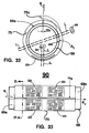
- FIGS. 32 and 33 after the compliant assembly 75 has been rolled onto the cylinder 69 , there may be an excess portion 75x of the compliant assembly 75 that must be trimmed so that a majority of the compliant assembly 75 can be smoothly rolled onto the cylinder 69 . As described above, there may be a gap 70g , if there is, then it is desirable to trim the excess portion 75x so that the gap 70g is as small as is practicable.
- a knife K or the like can be used to trim the excess 75x so that the compliant assembly 75 lays on the outer surface 69s without any bulges. In FIG. 33 , the knife K can cut along a direction K d to effectuate the trimming of the excess 75x to form a completely laminated cylinder 90 .
- the imprint stamps 20t are depicted in dashed outline because they are still positioned below the photopolymer shim 36 which have not been separated from the compliant media 70 .
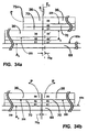
- FIG. 33 a line n-n thorough the cylinder 69 and the compliant assembly 75 is depicted in greater detail in a cross-sectional view in FIGS. 34a and 34b .
- FIG. 34a the compliant assembly 75 is depicted before the excess 75 x is trimmed.
- FIG. 34b the compliant assembly 75 is depicted after the excess 75x has been trimmed.
- the excess portion 75x comprises the compliant media 70 and the photopolymer shim 36 .
- the thin plastic film 33 that is connected with the photopolymer shim 36 may be opaque to light and the photopolymer shim 36 can be optically transparent
- the photopolymer shim 36 can be peeled back as denoted by the dashed arrow P so that the compliant media 70 (i.e. the optically transparent adhesive 51 and optically transparent compliant media 45 ) can be used to sight along an edge E s of the compliant assembly 75 that is already connected with the outer surface 69s of the cylinder 69 .
- a knife cut K along the sight line (see dashed line) for the edge E s can be used to trim off the excess 75x so that the unconnected layers of the excess 75x will align with their respective connected layers, that is: 33' to 33 ; 36' to 36; 45' to 45 ; and 51' to 51, as depicted in FIG. 34a. After the trimming, there may be the small gap 70g between adjacent ends of the compliant assembly 75 .
- the compliant assembly 75 forms an almost continuous layer on the outer surface 69s of the cylinder 69 .
- the photopolymer shim 36 can be peeled back P to expose the imprint stamp 20t on the compliant media 70 .
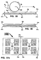
- the compliant assembly 75 is applied to a belt material 81 .
- the second backing 55 Prior to applying the compliant assembly 75 to the belt material 81 , the second backing 55 is peeled off of the transfer adhesive layer 51 to expose the second adhesive surface A 2 . Then the second adhesive surface A 2 is progressively applied to a surface 81a of the belt material 81 .
- a roller 89 such as a rubber roller, can be used to roll R the compliant assembly 75 in a roll direction R D .
- the rolling R can begin at a first end ( 75a, 81a ) and end at a second end ( 75b , 81b ) of the compliant assembly 75 and the belt material 81 .
- the first and second ends ( 81a, 81b ) can be joined to form a belt 100 as depicted in FIGS. 37a and 37b.
- a gap 70g may separate the first and second ends ( 75a , 75b ).
- Splicing tape or the like may be used to cover the gap 70g .
- a piece of splicing tape 81t can also be used to connect the first and second ends ( 81a, 81b ) of the belt material 81 to form the belt 100 .
- the photopolymer shim 36 i.e. the layer 33 and 36 of FIG. 28
- a suitable splicing tape includes but is not limited to a high temperature silicone based tape.
- the belt material 81 can be an optically transparent material so that light L can pass though the belt material 81, the compliant media 70 , and the imprint stamp 20t.
- a suitable optically transparent material for the belt material 81 includes but is not limited to a DuPont TM Mylar® .
- a light source 99 such as a ultraviolet light source, can be positioned inside or outside of the belt 100 to irradiate and cure a photopolymer material (not shown) that is urged into contact with the imprint stamp 20t .
- the belt material 81 can have a thickness t B from about 50.0 ⁇ m to about 150.0 ⁇ m.
Landscapes
- Engineering & Computer Science (AREA)
- Physics & Mathematics (AREA)
- Chemical & Material Sciences (AREA)
- General Physics & Mathematics (AREA)
- Nanotechnology (AREA)
- Manufacturing & Machinery (AREA)
- Crystallography & Structural Chemistry (AREA)
- Condensed Matter Physics & Semiconductors (AREA)
- Microelectronics & Electronic Packaging (AREA)
- Mathematical Physics (AREA)
- Theoretical Computer Science (AREA)
- Shaping Of Tube Ends By Bending Or Straightening (AREA)
- Exposure Of Semiconductors, Excluding Electron Or Ion Beam Exposure (AREA)
Applications Claiming Priority (2)
| Application Number | Priority Date | Filing Date | Title |
|---|---|---|---|
| US425891 | 1989-10-23 | ||
| US10/425,891 US6808646B1 (en) | 2003-04-29 | 2003-04-29 | Method of replicating a high resolution three-dimensional imprint pattern on a compliant media of arbitrary size |
Publications (2)
| Publication Number | Publication Date |
|---|---|
| EP1477849A2 true EP1477849A2 (de) | 2004-11-17 |
| EP1477849A3 EP1477849A3 (de) | 2005-07-27 |
Family
ID=33029751
Family Applications (1)
| Application Number | Title | Priority Date | Filing Date |
|---|---|---|---|
| EP03027335A Withdrawn EP1477849A3 (de) | 2003-04-29 | 2003-11-26 | Methode zur Reproduktion eines dreidimensionalen Prägemusters in einem Empfangsmaterial unbestimmter Grösse |
Country Status (5)
| Country | Link |
|---|---|
| US (1) | US6808646B1 (de) |
| EP (1) | EP1477849A3 (de) |
| JP (1) | JP4303638B2 (de) |
| CN (1) | CN1542550A (de) |
| TW (1) | TW200503067A (de) |
Cited By (3)
| Publication number | Priority date | Publication date | Assignee | Title |
|---|---|---|---|---|
| EP1801649A3 (de) * | 2005-12-21 | 2009-07-08 | ASML Netherlands B.V. | Imprint-Lithographie |
| WO2011028060A3 (en) * | 2009-09-03 | 2011-05-26 | Lg Electronics Inc. | Method for manufacturing a master mold which is used to form a micropatterned film applied to an exterior of a household appliance and manufacturing apparatus and method of the film using the master mold |
| KR101611286B1 (ko) | 2009-09-03 | 2016-04-11 | 엘지전자 주식회사 | 가전제품의 외면에 부착되는 필름에 미세 패턴을 형성하기 위한 마스터 몰드의 제조방법과 이를 이용하여 미세 패턴 필름을 제조하는 장치 및 방법 그리고 미세 패턴 필름이 부착된 가전제품 |
Families Citing this family (52)
| Publication number | Priority date | Publication date | Assignee | Title |
|---|---|---|---|---|
| KR100827741B1 (ko) | 2000-07-17 | 2008-05-07 | 보드 오브 리전츠, 더 유니버시티 오브 텍사스 시스템 | 임프린트 리소그래피 공정을 위한 자동 유체 분배 방법 및시스템 |
| US7179079B2 (en) * | 2002-07-08 | 2007-02-20 | Molecular Imprints, Inc. | Conforming template for patterning liquids disposed on substrates |
| US20080160129A1 (en) | 2006-05-11 | 2008-07-03 | Molecular Imprints, Inc. | Template Having a Varying Thickness to Facilitate Expelling a Gas Positioned Between a Substrate and the Template |
| US20040250683A1 (en) * | 2002-10-18 | 2004-12-16 | Innovative Construction And Building Materials, Llc | Advanced filtration devices and methods |
| ATE487579T1 (de) * | 2003-05-14 | 2010-11-15 | Molecular Imprints Inc | Verfahren, system, halter und anordnung zur übertragung von templates bei imprint- lithographieverfahren |
| JP2004354484A (ja) * | 2003-05-27 | 2004-12-16 | Alps Electric Co Ltd | 反射体の製造方法及び反射体製造装置 |
| EP1694731B1 (de) | 2003-09-23 | 2012-03-28 | University Of North Carolina At Chapel Hill | Photohärtbare perfluorpolyether zur verwendung als neue werkstoffe in mikrofluidischen vorrichtungen |
| US7150844B2 (en) * | 2003-10-16 | 2006-12-19 | Seagate Technology Llc | Dry passivation process for stamper/imprinter family making for patterned recording media |
| US9040090B2 (en) | 2003-12-19 | 2015-05-26 | The University Of North Carolina At Chapel Hill | Isolated and fixed micro and nano structures and methods thereof |
| MXPA06006738A (es) | 2003-12-19 | 2006-08-31 | Univ North Carolina | Metodos para fabricar micro- y nano-estructuras aisladas utilizando litografia suave o de impresion. |
| US7140861B2 (en) * | 2004-04-27 | 2006-11-28 | Molecular Imprints, Inc. | Compliant hard template for UV imprinting |
| US7785526B2 (en) | 2004-07-20 | 2010-08-31 | Molecular Imprints, Inc. | Imprint alignment method, system, and template |
| US7202179B2 (en) * | 2004-12-22 | 2007-04-10 | Hewlett-Packard Development Company, L.P. | Method of forming at least one thin film device |
| US7676088B2 (en) * | 2004-12-23 | 2010-03-09 | Asml Netherlands B.V. | Imprint lithography |
| US7686970B2 (en) | 2004-12-30 | 2010-03-30 | Asml Netherlands B.V. | Imprint lithography |
| US7585424B2 (en) * | 2005-01-18 | 2009-09-08 | Hewlett-Packard Development Company, L.P. | Pattern reversal process for self aligned imprint lithography and device |
| US7521313B2 (en) * | 2005-01-18 | 2009-04-21 | Hewlett-Packard Development Company, L.P. | Thin film device active matrix by pattern reversal process |
| US20060177535A1 (en) * | 2005-02-04 | 2006-08-10 | Molecular Imprints, Inc. | Imprint lithography template to facilitate control of liquid movement |
| EP1853967A4 (de) * | 2005-02-03 | 2009-11-11 | Univ North Carolina | Polymermaterial mit niedriger oberflächenenergie zur verwendung in flüssigkristallanzeigen |
| TWI251266B (en) * | 2005-03-11 | 2006-03-11 | Ind Tech Res Inst | Manufacturing method of the microstructure for roller and the structure thereof |
| KR100645641B1 (ko) | 2005-05-17 | 2006-11-14 | 삼성전기주식회사 | Ptfe를 이용한 인쇄회로기판용 임프린트 몰드 및 그제조방법 |
| US7341893B2 (en) * | 2005-06-02 | 2008-03-11 | Hewlett-Packard Development Company, L.P. | Structure and method for thin film device |
| US7994509B2 (en) * | 2005-11-01 | 2011-08-09 | Hewlett-Packard Development Company, L.P. | Structure and method for thin film device with stranded conductor |
| EP1905065B1 (de) * | 2005-06-20 | 2014-08-13 | Microcontinuum, Inc. | Mustererstellung von rolle zu rolle |
| WO2007133235A2 (en) * | 2005-08-08 | 2007-11-22 | Liquidia Technologies, Inc. | Micro and nano-structure metrology |
| EP2537657A3 (de) | 2005-08-09 | 2016-05-04 | The University of North Carolina At Chapel Hill | Verfahren und Materialien zur Herstellung mikrofluidischer Vorrichtungen |
| US8128393B2 (en) | 2006-12-04 | 2012-03-06 | Liquidia Technologies, Inc. | Methods and materials for fabricating laminate nanomolds and nanoparticles therefrom |
| US20080271625A1 (en) * | 2007-01-22 | 2008-11-06 | Nano Terra Inc. | High-Throughput Apparatus for Patterning Flexible Substrates and Method of Using the Same |
| US7795062B2 (en) * | 2007-04-03 | 2010-09-14 | Hewlett-Packard Development Company, L.P. | Method of forming a pressure switch thin film device |
| US20090108397A1 (en) * | 2007-10-31 | 2009-04-30 | Warren Jackson | Thin film device with layer isolation structure |
| US7906274B2 (en) * | 2007-11-21 | 2011-03-15 | Molecular Imprints, Inc. | Method of creating a template employing a lift-off process |
| US8765252B2 (en) | 2007-11-30 | 2014-07-01 | Hewlett-Packard Development Company, L.P. | Thin film device with minimized spatial variation of local mean height |
| US8518633B2 (en) | 2008-01-22 | 2013-08-27 | Rolith Inc. | Large area nanopatterning method and apparatus |
| US8182982B2 (en) * | 2008-04-19 | 2012-05-22 | Rolith Inc | Method and device for patterning a disk |
| US8192920B2 (en) * | 2008-04-26 | 2012-06-05 | Rolith Inc. | Lithography method |
| US8312609B2 (en) * | 2008-07-23 | 2012-11-20 | Seagate Technology, Llc | Method of manufacturing a patterned media stamper |
| US20100055346A1 (en) * | 2008-09-02 | 2010-03-04 | Seagate Technology Llc | PECVD RELEASE LAYER FOR Ni TEMPLATE |
| US20110210480A1 (en) * | 2008-11-18 | 2011-09-01 | Rolith, Inc | Nanostructures with anti-counterefeiting features and methods of fabricating the same |
| TW201038413A (en) * | 2009-04-29 | 2010-11-01 | Pegatron Corp | Manufacture method of micro pattern structure and case |
| KR101274713B1 (ko) * | 2009-12-07 | 2013-06-12 | 엘지디스플레이 주식회사 | 인쇄판의 제조 방법 및 그를 이용한 박막 패턴의 제조 방법 |
| CN102139856A (zh) * | 2010-02-01 | 2011-08-03 | 鸿富锦精密工业(深圳)有限公司 | 滚筒治具 |
| JP2014501934A (ja) | 2010-08-23 | 2014-01-23 | ローイス インコーポレイテッド | 近接場リソグラフィのためのマスク及びその製造方法 |
| WO2012122628A1 (en) | 2011-03-15 | 2012-09-20 | National Research Council Of Canada | Microfluidic system having monolithic nanoplasmonic structures |
| US8790561B2 (en) * | 2011-07-18 | 2014-07-29 | Oracle International Corporation | Methods for manufacturing an embosser drum for use in pre-formatting optical tape media |
| US10335322B2 (en) | 2013-08-26 | 2019-07-02 | Lightside Md, Llc | Adhesive support devices and methods of making and using them |
| US10786652B2 (en) | 2013-10-18 | 2020-09-29 | Lightside Md, Llc | Support devices and methods of making and using them |
| CN106750473B (zh) * | 2016-12-02 | 2019-09-03 | 江南大学 | 一种采用室温反压印技术制备高分辨率热塑性聚合物图案的方法 |
| WO2018191383A1 (en) * | 2017-04-11 | 2018-10-18 | Carpe Diem Technologies, Inc. | System and method of manufacturing a cylindrical nanoimprint lithography master |
| WO2020052749A1 (en) * | 2018-09-12 | 2020-03-19 | Applied Materials, Inc. | Method of manufacturing a stamp for imprint lithography, stamp for imprint lithography, imprint roller and roll-to-roll substrate processing apparatus |
| US12297367B2 (en) * | 2020-08-27 | 2025-05-13 | Applied Materials, Inc. | Encapsulation materials for flat optical devices |
| EP4248272B1 (de) * | 2020-12-21 | 2024-02-28 | 3M Innovative Properties Company | Gruppierte strukturierte replikationsartikel und verfahren |
| CN112731763B (zh) * | 2020-12-31 | 2024-10-01 | 嘉兴驭光光电科技有限公司 | 一种微纳光学器件制造方法 |
Family Cites Families (15)
| Publication number | Priority date | Publication date | Assignee | Title |
|---|---|---|---|---|
| GB9320326D0 (en) * | 1993-10-01 | 1993-11-17 | Ici Plc | Organic optical components and preparation thereof |
| US6180239B1 (en) * | 1993-10-04 | 2001-01-30 | President And Fellows Of Harvard College | Microcontact printing on surfaces and derivative articles |
| GB9509487D0 (en) | 1995-05-10 | 1995-07-05 | Ici Plc | Micro relief element & preparation thereof |
| GB9623185D0 (en) | 1996-11-09 | 1997-01-08 | Epigem Limited | Improved micro relief element and preparation thereof |
| GB9918617D0 (en) | 1999-08-07 | 1999-10-13 | Epigem Limited | An optical display composite |
| US6517995B1 (en) * | 1999-09-14 | 2003-02-11 | Massachusetts Institute Of Technology | Fabrication of finely featured devices by liquid embossing |
| US20030104614A1 (en) * | 2000-02-11 | 2003-06-05 | Uhrich Kathryn E. | Micropatterning surfaces of polymeric substrates |
| US6380101B1 (en) * | 2000-04-18 | 2002-04-30 | International Business Machines Corporation | Method of forming patterned indium zinc oxide and indium tin oxide films via microcontact printing and uses thereof |
| EP1297387A2 (de) * | 2000-06-30 | 2003-04-02 | President And Fellows of Harvard College | Elektrisches mikro-kontaktdruckverfahren und entsprechendes gerät |
| US6663820B2 (en) * | 2001-03-14 | 2003-12-16 | The Procter & Gamble Company | Method of manufacturing microneedle structures using soft lithography and photolithography |
| US20020130444A1 (en) * | 2001-03-15 | 2002-09-19 | Gareth Hougham | Post cure hardening of siloxane stamps for microcontact printing |
| US6817293B2 (en) * | 2001-03-28 | 2004-11-16 | Dainippon Printing Co., Ltd. | Patterning method with micro-contact printing and its printed product |
| US6645293B2 (en) * | 2002-03-07 | 2003-11-11 | Illinois Institute Of Technology | Molecular crystals of controlled size |
| US6656308B2 (en) * | 2002-04-22 | 2003-12-02 | International Business Machines Corporation | Process of fabricating a precision microcontact printing stamp |
| US6805809B2 (en) * | 2002-08-28 | 2004-10-19 | Board Of Trustees Of University Of Illinois | Decal transfer microfabrication |
-
2003
- 2003-04-29 US US10/425,891 patent/US6808646B1/en not_active Expired - Lifetime
- 2003-11-26 EP EP03027335A patent/EP1477849A3/de not_active Withdrawn
- 2003-11-28 TW TW092133560A patent/TW200503067A/zh unknown
-
2004
- 2004-02-27 CN CNA2004100076435A patent/CN1542550A/zh active Pending
- 2004-04-22 JP JP2004126881A patent/JP4303638B2/ja not_active Expired - Fee Related
Cited By (5)
| Publication number | Priority date | Publication date | Assignee | Title |
|---|---|---|---|---|
| EP1801649A3 (de) * | 2005-12-21 | 2009-07-08 | ASML Netherlands B.V. | Imprint-Lithographie |
| WO2011028060A3 (en) * | 2009-09-03 | 2011-05-26 | Lg Electronics Inc. | Method for manufacturing a master mold which is used to form a micropatterned film applied to an exterior of a household appliance and manufacturing apparatus and method of the film using the master mold |
| EP2473329A4 (de) * | 2009-09-03 | 2013-11-27 | Lg Electronics Inc | Verfahren zur herstellung einer masterform zur formung eines mikrostrukturierten films zur aufbringung auf der aussenseite einer haushaltanwendung sowie vorrichtung und verfahren zur herstellung des films mit der masterform |
| US8840795B2 (en) | 2009-09-03 | 2014-09-23 | Lg Electronics Inc. | Method for manufacturing a master mold which is used to form a micropatterned film applied to an exterior of a household appliance and manufacturing apparatus and method of the film using the master mold |
| KR101611286B1 (ko) | 2009-09-03 | 2016-04-11 | 엘지전자 주식회사 | 가전제품의 외면에 부착되는 필름에 미세 패턴을 형성하기 위한 마스터 몰드의 제조방법과 이를 이용하여 미세 패턴 필름을 제조하는 장치 및 방법 그리고 미세 패턴 필름이 부착된 가전제품 |
Also Published As
| Publication number | Publication date |
|---|---|
| CN1542550A (zh) | 2004-11-03 |
| JP2004327994A (ja) | 2004-11-18 |
| EP1477849A3 (de) | 2005-07-27 |
| TW200503067A (en) | 2005-01-16 |
| US20040217085A1 (en) | 2004-11-04 |
| US6808646B1 (en) | 2004-10-26 |
| JP4303638B2 (ja) | 2009-07-29 |
Similar Documents
| Publication | Publication Date | Title |
|---|---|---|
| US6808646B1 (en) | Method of replicating a high resolution three-dimensional imprint pattern on a compliant media of arbitrary size | |
| US7070406B2 (en) | Apparatus for embossing a flexible substrate with a pattern carried by an optically transparent compliant media | |
| US8016585B2 (en) | Nanoimprint resin stamper | |
| US7997890B2 (en) | Device and method for lithography | |
| TWI335490B (en) | Nano-imprinting process | |
| JP5982996B2 (ja) | 異物除去方法 | |
| JP7637816B2 (ja) | スタンプを剥離する方法および装置 | |
| CN113490883A (zh) | 大面积无缝母板和压印印模制造方法 | |
| TW201544447A (zh) | 用於凸印一奈米結構之方法及裝置 | |
| JP7326876B2 (ja) | 樹脂製モールド、レプリカモールドの製造方法、及び光学素子の製造方法 | |
| CN110989291B (zh) | 用于在光学构件的拱曲的面上制造(亚)微结构的方法以及光学构件 | |
| US20240053677A1 (en) | Apparatus and Method for Structured Replication and Transfer | |
| JP7507958B2 (ja) | ナノインプリントスタンプ | |
| HK1069214A (en) | Method of replicating a high resolution three-dimensional imprint pattern on a compliant media of arbitrary size | |
| KR101551772B1 (ko) | Scil 공정용 레플리카 스탬프 및 이의 제조방법 | |
| HK1069152A (en) | Apparatus for embossing a flexible substrate with a pattern carried by an optically transparent compliant media | |
| TW202421449A (zh) | 多紋理印模 | |
| HK1114185B (en) | Method for imprint lithography at constant temperature | |
| HK1114185A1 (en) | Method for imprint lithography at constant temperature |
Legal Events
| Date | Code | Title | Description |
|---|---|---|---|
| PUAI | Public reference made under article 153(3) epc to a published international application that has entered the european phase |
Free format text: ORIGINAL CODE: 0009012 |
|
| 17P | Request for examination filed |
Effective date: 20040705 |
|
| AK | Designated contracting states |
Kind code of ref document: A2 Designated state(s): AT BE BG CH CY CZ DE DK EE ES FI FR GB GR HU IE IT LI LU MC NL PT RO SE SI SK TR |
|
| AX | Request for extension of the european patent |
Extension state: AL LT LV MK |
|
| PUAL | Search report despatched |
Free format text: ORIGINAL CODE: 0009013 |
|
| AK | Designated contracting states |
Kind code of ref document: A3 Designated state(s): AT BE BG CH CY CZ DE DK EE ES FI FR GB GR HU IE IT LI LU MC NL PT RO SE SI SK TR |
|
| AX | Request for extension of the european patent |
Extension state: AL LT LV MK |
|
| RIC1 | Information provided on ipc code assigned before grant |
Ipc: 7B 29C 59/02 B Ipc: 7G 03F 7/20 B Ipc: 7G 03F 7/00 A |
|
| D17P | Request for examination filed (deleted) | ||
| AKX | Designation fees paid | ||
| STAA | Information on the status of an ep patent application or granted ep patent |
Free format text: STATUS: THE APPLICATION IS DEEMED TO BE WITHDRAWN |
|
| 18D | Application deemed to be withdrawn |
Effective date: 20060128 |
|
| REG | Reference to a national code |
Ref country code: DE Ref legal event code: 8566 |