EP1473835B1 - Per-element resampling for a digital-to-analog converter - Google Patents
Per-element resampling for a digital-to-analog converter Download PDFInfo
- Publication number
- EP1473835B1 EP1473835B1 EP03029342A EP03029342A EP1473835B1 EP 1473835 B1 EP1473835 B1 EP 1473835B1 EP 03029342 A EP03029342 A EP 03029342A EP 03029342 A EP03029342 A EP 03029342A EP 1473835 B1 EP1473835 B1 EP 1473835B1
- Authority
- EP
- European Patent Office
- Prior art keywords
- analog
- resampling
- analog output
- signals
- partial
- Prior art date
- Legal status (The legal status is an assumption and is not a legal conclusion. Google has not performed a legal analysis and makes no representation as to the accuracy of the status listed.)
- Expired - Lifetime
Links
- 238000012952 Resampling Methods 0.000 title claims description 68
- 238000000034 method Methods 0.000 claims description 12
- 230000005540 biological transmission Effects 0.000 claims description 10
- 230000004044 response Effects 0.000 claims description 6
- 230000001105 regulatory effect Effects 0.000 claims description 5
- 230000003213 activating effect Effects 0.000 claims description 4
- 238000006243 chemical reaction Methods 0.000 claims description 2
- 238000010586 diagram Methods 0.000 description 9
- 230000007704 transition Effects 0.000 description 3
- 230000001934 delay Effects 0.000 description 2
- 230000008859 change Effects 0.000 description 1
- 230000001010 compromised effect Effects 0.000 description 1
- 230000001276 controlling effect Effects 0.000 description 1
- 230000003111 delayed effect Effects 0.000 description 1
- 239000006185 dispersion Substances 0.000 description 1
- 238000012886 linear function Methods 0.000 description 1
- 229910044991 metal oxide Inorganic materials 0.000 description 1
- 150000004706 metal oxides Chemical class 0.000 description 1
- 239000000203 mixture Substances 0.000 description 1
- 230000003071 parasitic effect Effects 0.000 description 1
- 230000008569 process Effects 0.000 description 1
- 239000004065 semiconductor Substances 0.000 description 1
- 230000003595 spectral effect Effects 0.000 description 1
Images


Classifications
-
- H—ELECTRICITY
- H03—ELECTRONIC CIRCUITRY
- H03M—CODING; DECODING; CODE CONVERSION IN GENERAL
- H03M1/00—Analogue/digital conversion; Digital/analogue conversion
- H03M1/06—Continuously compensating for, or preventing, undesired influence of physical parameters
- H03M1/0617—Continuously compensating for, or preventing, undesired influence of physical parameters characterised by the use of methods or means not specific to a particular type of detrimental influence
- H03M1/0624—Continuously compensating for, or preventing, undesired influence of physical parameters characterised by the use of methods or means not specific to a particular type of detrimental influence by synchronisation
-
- H—ELECTRICITY
- H03—ELECTRONIC CIRCUITRY
- H03M—CODING; DECODING; CODE CONVERSION IN GENERAL
- H03M1/00—Analogue/digital conversion; Digital/analogue conversion
- H03M1/06—Continuously compensating for, or preventing, undesired influence of physical parameters
- H03M1/08—Continuously compensating for, or preventing, undesired influence of physical parameters of noise
- H03M1/0863—Continuously compensating for, or preventing, undesired influence of physical parameters of noise of switching transients, e.g. glitches
- H03M1/0872—Continuously compensating for, or preventing, undesired influence of physical parameters of noise of switching transients, e.g. glitches by disabling changes in the output during the transitions, e.g. by holding or latching
-
- H—ELECTRICITY
- H03—ELECTRONIC CIRCUITRY
- H03M—CODING; DECODING; CODE CONVERSION IN GENERAL
- H03M1/00—Analogue/digital conversion; Digital/analogue conversion
- H03M1/66—Digital/analogue converters
- H03M1/74—Simultaneous conversion
Definitions
- the invention relates generally to circuits, and more particularly to a digital-to-analog converter.
- Digital-to-analog converters are circuits that receive digital inputs and produce analog outputs that are analog equivalents of the digital inputs in the form of currents or voltages.
- a typical DAC includes an encoder, a number of analog output elements and a summing circuit.
- the encoder receives a digital input, which is a digital value represented by a number of binary data bits, and then encodes the binary data bits into suitable drive signals to selectively activate the analog output elements.
- the activated analog output elements generate partial analog signals. These partial analog signals are then combined by the summing circuit to produce an analog output, which is an analog representation of the digital input.
- glitches A problem that often arises during the operation of a DAC is the appearance of output errors called “glitches”, which are mainly caused by mistiming of the partial analog signals at the output of the DAC. These glitches do not affect the final, settled value of the analog output for each digital input, and appear only during the transition from one digital input to the next. Therefore, the glitches corrupt the spectral content of the output signal, which presents an important concern for high-speed applications since the glitches can be misinterpreted as analog outputs.
- mistiming is different arrival times of the data bits of a digital input at the input of the encoder. However, this mistiming source can be easily minimized by using latches at the input of the encoder to synchronize the data bits.
- Another source of mistiming is differential logic delay between the input of the encoder and the output of the encoder. Again, this mistiming source can be minimized by adding latches at the output of the encoder with a carefully controlled clock.
- Still another source of mistiming is mismatch of path lengths between the encoder and the output analog elements and/or mismatch of path lengths between the output analog elements and the output of the DAC through the summing circuit.
- This last source of mistiming can be minimized by adding a switch between the summing circuit and the output of the DAC.
- the switch is used to pass the analog signal to the output only after the signal has settled to a final value.
- This technique returns the output waveform to zero or some reference value during the problematic time, and thus, is commonly referred to as "Return to Zero" or RZ.
- the mismatched delays before the summing unit no longer affect the high-speed performance of the DAC, and the signal integrity becomes limited primarily by the linearity of the switch and the purity of a resampling clock used to operate the switch. Between these two limiting factors, the linearity of the switch is the main limiting factor. Switch nonlinearity can be due to the series resistance of the switch, which may have a nonlinear function with respect to the current passing through the switch. Furthermore, the switch nonlinearity may be due to other nonlinear parasitics, such as capacitance, which vary with current levels.
- the digital-to-analog converter described in US 4,663,610 comprises two shift registers, each shift register controlling three structural current sources providing the same current.
- the output signal of the converter is a time-continuous addition of the switched current sources depending on the serial digital data traversing through the shift registers.
- a DAC is described for parallel digital data of a word length ofN, the converter comprising 2 N switched current sources. All current sources provide the same amount of current, whereby the output current of the converter is selected by the number of switched current sources.
- An anti-glitch circuit for 2 N current sources is used to reduce the delayed dispersion among the 2 N switches by adding individual delays to the individual anti-glitch signals.
- a digital-to-analog converter (DAC) and method for converting digital inputs into analog outputs utilizes resampling switches to regulate the transmission of partial analog signals between analog output elements and a summing circuit to reduce or eliminate "glitches" in the output signal.
- Each resampling switch may be individually connected to an analog output element to handle a fixed partial analog signal, e.g., a fixed current, generated by that analog output element. Consequently, the resampling switches can be used to reduce or eliminate the glitches in the output signal without introducing switch nonlinearity into the output signal by simultaneously transmitting the partial analog signals to the summing circuit using the resampling switches.
- a DAC in accordance with an embodiment of the invention includes a number of analog output elements, a number of switches and a summing circuit.
- the analog output elements are configured to selectively generate partial analog signals in response to a digital input.
- the summing circuit is configured to combine the partial analog signals to produce an analog output, which is an analog representation of the digital input.
- the switches are located between the analog output elements and the summing circuit to regulate the transmission of the partial analog signals between the analog output elements and the summing circuit. Each switch may be connected to a distinct analog output element to transmit the partial analog signal generated by that analog output element to the summing circuit.
- a method for converting digital inputs into analog outputs in accordance with an embodiment of the invention includes receiving a digital input, generating partial analog signals in response to the digital input, regulating the transmission of the partial analog signals, and receiving and combining the partial analog signals to produce an analog output, which is an analog representation of the digital input.
- Fig. 1 is a diagram of a digital-to-analog converter (DAC) in accordance with an exemplary embodiment of the invention.
- DAC digital-to-analog converter
- Fig. 2 is a partial diagram of a DAC configured in a standard segmented DAC architecture in accordance with an embodiment of the invention.
- Fig. 3 is a circuit diagram of an analog output element and a resampling switch, which can be use in the DAC of Fig. 1 or 2 , in accordance with an exemplary implementation.
- Fig. 4 is a timing diagram of the analog output element and the resampling switch of Fig.3
- Fig. 5 is a process flow diagram of a method for converting digital inputs into analog outputs in accordance with an exemplary embodiment of the invention.
- a digital-to-analog converter (DAC) 100 in accordance with an exemplary embodiment of the invention is shown.
- the DAC 100 operates to produce analog outputs in response to received digital inputs.
- the magnitudes of the analog outputs correspond to the values represented by the respective digital inputs.
- the analog outputs are analog equivalents of the digital inputs.
- the DAC 100 includes an encoder 102, analog output elements 104 (only five analog output elements 104A, 104B, 104C, 104D and 104E are illustrated in Fig. 1 ), resampling switches 106 and a summing unit 108. As shown in Fig.
- the resampling switches 106 are positioned between the analog output elements 104 and the summing unit 108. As described below, the use of these resampling switches 106 reduces or eliminates output errors known as "glitches" in the output signal of the DAC 100 without introducing switch nonlinearity, which is a common concern with conventional DACs using a "Return to Zero” (RZ) technique. Thus, the integrity of the output signal is not compromised by the use of the resampling switches 106 to reduce or eliminate glitches in the output signal.
- RZ Return to Zero
- the encoder 102 of the DAC 100 operates to translate N binary data bits of a received digital input into M encoded signals, where N and M are integers.
- the encoder 102 is connected to N input lines 110 to receive the N binary data bits.
- the encoder 102 is also connected to M control lines 112, which are individually connected to the analog output elements 104, to transmit the M encoded signals from the encoder to the analog output elements through the M control lines.
- the M encoded signals are drive signals that are used to selectively activate the analog output elements 104 in accordance with the value of the digital input so that an equivalent analog output can be produced using the analog signals generated by the activated analog output elements.
- Each encoded signal is either an enable signal to activate an analog output element or a disable signal to deactivate an analog output element.
- the encoder 102 may be any encoder that can be used in a DAC to translate binary data bits into encoded signals.
- the encoder 102 may be a standard thermometer encoder that uses a look-up table to translate binary data bits into thermometer-encoded signals.
- the analog output elements 104 of the DAC 100 operate to generate one or more analog signals when the elements are selectively activated by the encoded signals from the encoder 102.
- the analog signals generated by the analog output elements 104 are partial analog signals that are subsequently combined to produce an analog output.
- the analog output elements 104 may be configured to generate the analog signals in the form of currents.
- the analog output elements 104 are individually connected to the encoder 102 via the control lines 112 to receive encoded signals for a given digital input. That is, each analog output element 104 is connected to the encoder 102 by a separate control line 112 to receive one of the encoded signals for the given digital input.
- the connected analog output element 104 is activated so that a partial analog signal is generated, or deactivated so that no signal is generated.
- the analog output elements 104 are identical, and thus, each analog output element generates the same analog signal, e.g., the same current, when activated by an enable encoded signal.
- the output of each analog output element 104 is connected to the summing circuit 108 through one of the resampling switches 106.
- the resampling switches 106 of the DAC 100 operate to simultaneously transmit the partial analog signals generated by the activated analog output elements 104 to the summing circuit 108 using a resampling clock signal Clk .
- Each resampling switch 106 is individually connected to a distinct analog output element 104 to transmit the partial analog signal generated by that analog output element.
- the number of resampling switches is equal to the number of analog output elements 104.
- the Clk signal controls the state of the resampling switches 106 to simultaneously close or open all the resampling switches for a given period.
- the resampling switches 106 regulate the transmission of the partial analog signals between the activated analog output elements 104 to the summing circuit 108.
- the resampling switches 106 perform a similar function to a conventional RZ switch.
- the resampling switches 106 can be operated to allow partial analog signals, e.g., currents, to settle to the final value before being transmitted to the summing circuit 108. Consequently, the portions of the analog signals that contribute to glitches in the final output signal of the DAC 100 are effectively removed by the use of the resampling switches 106.
- the resampling switches 106 are identical, as is the case for the analog output elements 104. Thus, when closed, each resampling switch 106 connected to an activated analog output element 104 passes the analog signal generated by that analog output element.
- each resampling switch 106 handles a fixed analog signal, e.g., a fixed current, the concern with respect to switch nonlinearity, which is a significant concern in using a conventional RZ switch, is resolved by using the resampling switches to simultaneously transmit equivalent analog signals from the analog output elements 104 to the summing circuit 108.
- the DAC 100 may include fewer resampling switches 106 than the number of analog output elements 104.
- the outputs of two or more analog output elements 104 may be connected to each other such that partial analog signals from the analog output elements are combined. The resulting output is also connected to the input of one of the resampling switches 106.
- each resampling switch 106 can be connected to transmit a combined analog signal from multiple analog output elements 104.
- the number of resampling switches 106 included in the DAC 100 may be any number less than the total number of analog output elements 104 included in the DAC.
- the summing circuit 108 of the DAC 100 operates to combine the partial analog signals from the analog output elements 104, which are simultaneously transmitted through the resampling switches 106, to produce an analog output on an output terminal 114, which is an analog equivalent of the received digital input.
- the summing circuit 108 may be configured to produce the analog output using one of various signal combining schemes that linearly add the analog signals from the analog output elements 104.
- the summing circuit 108 may use a standard segmented current summing scheme in which some of the currents (i.e., the partial analog signals) from the analog output elements 104 are directly applied to the output terminal 114 to provide most significant bit signals of the analog output, while other currents from the analog output elements are first scaled using an R-2R structure before being applied to the output terminal to provide binary-scaled least significant bit signals of the analog output.
- Other current summing schemes which may be used by the summing circuit 108, include a straight binary-weighted R-2R scheme and a single output load resistor scheme in which the currents from the analog output elements 104 are applied to a single output load resistor.
- the output terminal 114 of the DAC 100 may be connected to a current-to-voltage converter (not shown) to change the analog output from a current to a voltage.
- the signal After being combined at the summing circuit 108, if there are n 1's present in the control lines 112, the signal will be n * I 1 + ( M - n) * I 0 . This is a linear function of n , although the signal may include gain and offset errors.
- Fig. 2 part of a DAC 200 configured in a standard segmented DAC architecture in accordance with an embodiment of the invention is shown. Same reference numerals of Fig. 1 are used to identify similar elements in Fig. 2 . An encoder for the DAC 200 is not shown in Fig. 2 .
- the DAC 200 includes an R-2R output summing circuit 208, which is electrically connected to the analog output elements 104A, 104B, 104C, 104D and 104E via the resampling switches 106.
- each analog output element generates the same analog signal, e.g., the same current.
- the entire analog signal or a scaled portion of the analog signal from a particular analog output element may be transmitted to the output terminal 114 to produce the resulting analog output.
- analog output elements that are directly connected to the output terminal 114 e.g., the analog output elements 104A, 104B and 104C
- the entire analog signals generated by these analog output elements are transmitted to the output terminal 114.
- analog output elements that are connected to the output terminal 114 via one or more R and 2R resistors e.g., the analog output elements 104D and 104E
- binary-scaled portions of the analog signals generated by these analog output elements are transmitted to the output terminal 114.
- the analog output elements that are directly connected to the output terminal 114 can be considered as providing most significant bit (MSB) signals of an analog output, which are large fixed analog signals, while the analog output elements that are connected to the output terminal 114 via one or more R and 2R resistors can be considered as providing least significant bit (LSB) signals of the analog output, which are smaller scaled signals.
- MSB signals and the LSB signals are combined at the output terminal 114 to produce the analog output.
- only three analog output elements 104A, 104B and 104C for generating the MSB signals and two analog output elements 104D and 104E for generating LSB signals are shown in Fig. 2 .
- the number of analog output elements included in the DAC 200 to generate the required MSB and LSB signals to produce analog outputs can be significantly larger.
- the DAC 200 may include thirty-two (32) analog output elements to generate the MSB signals and nine (9) analog output elements to generate the LSB signals for a 14-bit digital-to-analog conversion.
- the DACs 100 and 200 of Figs. 1 and 2 have been illustrated and described as being configured to generate a single analog output for a given digital
- the DACs 100 and 200 can be modified to generate a pair of differential analog outputs for a given digital input, which may be desired for certain applications.
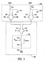
- an analog output element 304 and a resampling switch 306 in accordance with an exemplary differential implementation are shown.
- the analog output element 304 and the resampling switch 306 can be used in the DAC 100 of Fig. 1 or the DAC 200 of Fig. 2 .
- the analog output element 304 and the resampling switch 306 are configured to generate differential analog signals, I out and I out , using encoded signals, D and D , and resampling clock signals, Clk and Clk .
- the analog output element 304 includes differentially connected bipolar transistors 316 and 318 and a current source 320. The emitters of the differentially connected transistors 316 and 318 are connected to the current source 320.
- the base of the differentially connected transistor 316 is connected to receive the encoded signal D
- the base of the differentially connected transistor 318 is connected to receive the encoded signal D
- the current source 320 includes a bipolar transistor 322 and a resistor 324, which are connected in series to a low voltage terminal 326, e.g., -3.3V.
- the base of the bipolar transistor 322 is connected to receive a bias voltage V bias , which controls the current conducted through the transistor.
- the bipolar transistor 322 and the resistor 324 of the current source 320 operate to conduct a fixed current I source that defines the values of I out and I out .
- the differentially connected transistors 316 and 318 of the analog output element 304 are connected to the resampling switch 306, which includes bipolar resampling transistors 328, 330, 332 and 334.
- the emitters of the resampling transistors 328 and 330 are connected to the collector of the differentially connected transistor 316 of the analog output element 304, while the emitters of the resampling transistors 332 and 334 are connected to the collector of the other differentially connected transistor 318 of the analog output element.
- the collector of the resampling transistor 328 is also connected to a summing circuit 208A (not shown) to transmit the differential analog signal I out .
- the collector of the resampling transistor 332 is connected to another summing circuit 208B (not shown) to transmit the differential analog signal I out .
- the summing circuits 208A and 208B may be identical to the summing circuit 208 of Fig. 2 .
- the summing circuits 208A and 208B are configured to receive differential analog signals from analog output elements to produce differential analog outputs.
- the resampling transistors 328 and 332 are controlled by the clock signal Clk, which is applied to the bases of the transistors 328 and 332.
- the resampling transistors 330 and 334 are controlled by the clock signal Clk , which is applied to the bases of the transistors 330 and 334.
- the collectors of the resampling transistors 330 and 334 are connected to a voltage terminal 336, e.g., ground, to discard currents from the resampling transistors 330 and 334, which may be corrupted by glitchy transitions when the clock signal Clk is high.
- transistors of the analog output element 304 and the resampling switch 306 are illustrated and described as being bipolar transistors, other types of transistors may instead be used.
- the transistors of the analog output element 304 and the resampling switch 306 can be metal oxide semiconductor (MOS) transistors.
- MOS metal oxide semiconductor
- these transistors may be a mixture of different types of transistors.
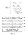
- a timing diagram for the signals, I out , I out , Clk and D are shown. These signals are examples to illustrate the operation of the analog output element 304 and the corresponding resampling switch 306. As shown in the timing diagram, a high differential signal I out is generated when both the clock signal Clk and the encoded signal D are high, while a high differential signal I out is generated when the clock signal Clk is high and the encoded signal D is low. As further shown in the timing diagram, the clock signal Clk is temporally offset from the encoded signal D so that the encoded signal D changes only while the clock signal Clk is low. Thus, the differential analog signals, I out and I out have a chance to settle before the clock signal Clk again rises, which results in clean output pulses.
- a method for converting digital inputs into analog outputs in accordance with an exemplary embodiment is described with reference to a flow diagram of Fig. 5 .
- input digital signals of a digital input are received.
- the input digital signals of the digital input represent a value.
- the input digital signals are translated into encoded signals.
- the encoded signals may be thermometer-encoded signals.
- partial analog signals are generated using the encoded signals.
- the partial analog signals may be generated by selectively activating analog output elements using the encoded signals as drive signals.
- the transmission of the partial analog signals is regulated.
- a number of resampling switches may be used to regulate the transmission of the partial analog signals by simultaneously closing and opening the resampling switches using a clock signal to simultaneously transmit the partial analog signals, which can reduce or eliminate glitches in the resulting output signal without introducing switch nonlinearity.
- the clock signal should be temporally offset from the transitions in the input digital signal so that relevant electrical signals have a chance to settle when the switches are open.
- the partial analog signals are received and combined using a predefined scheme to produce an analog output, which is an analog representation of the digital input.
- the partial analog signals may be combined using a standard segmented combining scheme using an R-2R structure.
Landscapes
- Engineering & Computer Science (AREA)
- Theoretical Computer Science (AREA)
- Analogue/Digital Conversion (AREA)
- Electronic Switches (AREA)
Applications Claiming Priority (2)
| Application Number | Priority Date | Filing Date | Title |
|---|---|---|---|
| US427578 | 2003-04-30 | ||
| US10/427,578 US6812878B1 (en) | 2003-04-30 | 2003-04-30 | Per-element resampling for a digital-to-analog converter |
Publications (3)
| Publication Number | Publication Date |
|---|---|
| EP1473835A2 EP1473835A2 (en) | 2004-11-03 |
| EP1473835A3 EP1473835A3 (en) | 2005-04-06 |
| EP1473835B1 true EP1473835B1 (en) | 2008-02-13 |
Family
ID=32990446
Family Applications (1)
| Application Number | Title | Priority Date | Filing Date |
|---|---|---|---|
| EP03029342A Expired - Lifetime EP1473835B1 (en) | 2003-04-30 | 2003-12-18 | Per-element resampling for a digital-to-analog converter |
Country Status (4)
| Country | Link |
|---|---|
| US (1) | US6812878B1 (enExample) |
| EP (1) | EP1473835B1 (enExample) |
| JP (1) | JP2004336772A (enExample) |
| DE (1) | DE60319065T2 (enExample) |
Families Citing this family (10)
| Publication number | Priority date | Publication date | Assignee | Title |
|---|---|---|---|---|
| US7042379B2 (en) * | 2004-07-30 | 2006-05-09 | Rockwell Scientific Licensing, Llc | Return-to-zero current switching digital-to-analog converter |
| US7023368B1 (en) * | 2004-08-31 | 2006-04-04 | Euvis, Inc. | Digital-to-analog signal converting apparatus and method to extend usable spectrum over Nyquist frequency |
| US8085178B2 (en) * | 2009-06-04 | 2011-12-27 | Bae Systems Information And Electronic Systems Integration Inc. | Multiplying-adding return to zero digital to analog converter circuit and method |
| JP5451317B2 (ja) * | 2009-10-29 | 2014-03-26 | 新日本無線株式会社 | 連続時間型多ビットδσadc回路 |
| US8125361B2 (en) | 2010-07-12 | 2012-02-28 | Teledyne Scientific & Imaging, Llc | Digital-to-analog converter (DAC) calibration system |
| US8406340B2 (en) * | 2011-01-14 | 2013-03-26 | Broadcom Corporation | Distortion and aliasing reduction for digital to analog conversion |
| US8659458B1 (en) * | 2012-10-11 | 2014-02-25 | Teledyne Scientific & Imaging, Llc | Multiple return-to-zero current switching digital-to-analog converter for RF signal generation |
| US8976050B1 (en) * | 2013-09-12 | 2015-03-10 | Fujitsu Semiconductor Limited | Circuitry and methods for use in mixed-signal circuitry |
| EP2849345B1 (en) * | 2013-09-12 | 2020-11-04 | Socionext Inc. | Circuitry and methods for use in mixed-signal circuitry |
| US9350377B1 (en) | 2015-07-07 | 2016-05-24 | Rohde & Schwarz Gmbh & Co. Kg | Digital-to-analog converter with local interleaving and resampling |
Family Cites Families (11)
| Publication number | Priority date | Publication date | Assignee | Title |
|---|---|---|---|---|
| US4321584A (en) * | 1979-06-15 | 1982-03-23 | Rockwell International Corporation | Charge coupled digital-to-analog converter |
| US4369432A (en) * | 1980-02-08 | 1983-01-18 | Takeda Riken Kogyo Kabushikikaisha | Auto-calibrated D-A converter |
| US4663610A (en) * | 1985-11-22 | 1987-05-05 | Tektronix, Inc. | Serial digital-to-analog converter |
| JPH0388426A (ja) * | 1989-06-29 | 1991-04-12 | Nec Corp | D/aコンバータ |
| JPH0344216A (ja) * | 1989-07-12 | 1991-02-26 | Toshiba Corp | D/a変換器 |
| KR0183767B1 (ko) * | 1995-12-14 | 1999-04-15 | 김광호 | 디지탈 데이타 레벨 조정 회로 |
| JPH10276093A (ja) * | 1997-03-28 | 1998-10-13 | Sony Corp | D/a変換器 |
| US6191719B1 (en) * | 1997-08-25 | 2001-02-20 | Broadcom Corporation | Digital to analog converter with reduced ringing |
| GB9803928D0 (en) * | 1998-02-26 | 1998-04-22 | Wolfson Ltd | Digital to analogue converters |
| US6292125B1 (en) * | 1999-09-29 | 2001-09-18 | Lsi Logic Corporation | Digital-to-analog converter using weights stored in a weight table |
| US6583744B2 (en) * | 2001-06-22 | 2003-06-24 | Texas Instruments Incorporated | Correction circuit for beta mismatch between thermometer encoded and R-2R ladder segments of a current steering DAC |
-
2003
- 2003-04-30 US US10/427,578 patent/US6812878B1/en not_active Expired - Lifetime
- 2003-12-18 EP EP03029342A patent/EP1473835B1/en not_active Expired - Lifetime
- 2003-12-18 DE DE60319065T patent/DE60319065T2/de not_active Expired - Lifetime
-
2004
- 2004-04-30 JP JP2004135316A patent/JP2004336772A/ja active Pending
Also Published As
| Publication number | Publication date |
|---|---|
| DE60319065T2 (de) | 2009-02-05 |
| JP2004336772A (ja) | 2004-11-25 |
| US6812878B1 (en) | 2004-11-02 |
| EP1473835A3 (en) | 2005-04-06 |
| DE60319065D1 (de) | 2008-03-27 |
| EP1473835A2 (en) | 2004-11-03 |
Similar Documents
| Publication | Publication Date | Title |
|---|---|---|
| US5243347A (en) | Monotonic current/resistor digital-to-analog converter and method of operation | |
| US6914547B1 (en) | Triple resistor string DAC architecture | |
| US6703956B1 (en) | Technique for improved linearity of high-precision, low-current digital-to-analog converters | |
| CN105210298B (zh) | 多串数模转换器 | |
| EP0493443B1 (en) | PARALLEL ANALOG-TO-DIGITAL CONVERTER USING 2?(n-1) COMPARATORS | |
| US5283580A (en) | Current/resistor digital-to-analog converter having enhanced integral linearity and method of operation | |
| US7511465B2 (en) | Digital pulse width modulated power supply with variable LSB | |
| US6977602B1 (en) | Wide band digital to analog converters and methods, including converters with selectable impulse response | |
| US5446455A (en) | Auto-calibrated current-mode digital-to-analog converter and method therefor | |
| JP2001244816A (ja) | 改善された線形性および整定時間を有するデジタルにスイッチングされる電位差計 | |
| CN111628770B (zh) | 用于时间交错adc的电流控制mdac以及相关方法 | |
| EP1473835B1 (en) | Per-element resampling for a digital-to-analog converter | |
| US7061421B1 (en) | Flash ADC with variable LSB | |
| US6191720B1 (en) | Efficient two-stage digital-to-analog converter using sample-and-hold circuits | |
| US6778122B2 (en) | Resistor string digital to analog converter with differential outputs and reduced switch count | |
| US7372387B2 (en) | Digital-to-analog converter with triode region transistors in resistor/switch network | |
| CN108702158B (zh) | 数模转换器和数模转换方法 | |
| US20050285770A1 (en) | High-speed current mode analog to digital converter | |
| CN111628771B (zh) | 基于mdac的时间交错模数转换器以及相关方法 | |
| US5748128A (en) | Reduced current quadratic digital/analog converter with improved settling-time | |
| US6501412B2 (en) | Analog-to-digital converter including a series of quantizers interconnected in cascade | |
| CN119814031A (zh) | 数模转换器系统 | |
| US20030201924A1 (en) | Digital-to-analog converter | |
| EP0135274A2 (en) | Digital-to-analog converter | |
| Boylston et al. | Enhancing performance in interpolating resistor string DACs |
Legal Events
| Date | Code | Title | Description |
|---|---|---|---|
| PUAI | Public reference made under article 153(3) epc to a published international application that has entered the european phase |
Free format text: ORIGINAL CODE: 0009012 |
|
| AK | Designated contracting states |
Kind code of ref document: A2 Designated state(s): AT BE BG CH CY CZ DE DK EE ES FI FR GB GR HU IE IT LI LU MC NL PT RO SE SI SK TR |
|
| AX | Request for extension of the european patent |
Extension state: AL LT LV MK |
|
| PUAL | Search report despatched |
Free format text: ORIGINAL CODE: 0009013 |
|
| AK | Designated contracting states |
Kind code of ref document: A3 Designated state(s): AT BE BG CH CY CZ DE DK EE ES FI FR GB GR HU IE IT LI LU MC NL PT RO SE SI SK TR |
|
| AX | Request for extension of the european patent |
Extension state: AL LT LV MK |
|
| 17P | Request for examination filed |
Effective date: 20050517 |
|
| AKX | Designation fees paid |
Designated state(s): DE FR GB |
|
| RAP1 | Party data changed (applicant data changed or rights of an application transferred) |
Owner name: AGILENT TECHNOLOGIES, INC. |
|
| GRAP | Despatch of communication of intention to grant a patent |
Free format text: ORIGINAL CODE: EPIDOSNIGR1 |
|
| GRAS | Grant fee paid |
Free format text: ORIGINAL CODE: EPIDOSNIGR3 |
|
| GRAA | (expected) grant |
Free format text: ORIGINAL CODE: 0009210 |
|
| AK | Designated contracting states |
Kind code of ref document: B1 Designated state(s): DE FR GB |
|
| REG | Reference to a national code |
Ref country code: GB Ref legal event code: FG4D |
|
| REF | Corresponds to: |
Ref document number: 60319065 Country of ref document: DE Date of ref document: 20080327 Kind code of ref document: P |
|
| EN | Fr: translation not filed | ||
| PLBE | No opposition filed within time limit |
Free format text: ORIGINAL CODE: 0009261 |
|
| STAA | Information on the status of an ep patent application or granted ep patent |
Free format text: STATUS: NO OPPOSITION FILED WITHIN TIME LIMIT |
|
| 26N | No opposition filed |
Effective date: 20081114 |
|
| PG25 | Lapsed in a contracting state [announced via postgrant information from national office to epo] |
Ref country code: FR Free format text: LAPSE BECAUSE OF FAILURE TO SUBMIT A TRANSLATION OF THE DESCRIPTION OR TO PAY THE FEE WITHIN THE PRESCRIBED TIME-LIMIT Effective date: 20081205 |
|
| PGFP | Annual fee paid to national office [announced via postgrant information from national office to epo] |
Ref country code: GB Payment date: 20081217 Year of fee payment: 6 |
|
| GBPC | Gb: european patent ceased through non-payment of renewal fee |
Effective date: 20091218 |
|
| PG25 | Lapsed in a contracting state [announced via postgrant information from national office to epo] |
Ref country code: GB Free format text: LAPSE BECAUSE OF NON-PAYMENT OF DUE FEES Effective date: 20091218 |
|
| REG | Reference to a national code |
Ref country code: DE Ref legal event code: R082 Ref document number: 60319065 Country of ref document: DE Representative=s name: SCHOPPE, ZIMMERMANN, STOECKELER, ZINKLER & PAR, DE |
|
| REG | Reference to a national code |
Ref country code: DE Ref legal event code: R082 Ref document number: 60319065 Country of ref document: DE Representative=s name: SCHOPPE, ZIMMERMANN, STOECKELER, ZINKLER, SCHE, DE Effective date: 20141028 Ref country code: DE Ref legal event code: R081 Ref document number: 60319065 Country of ref document: DE Owner name: KEYSIGHT TECHNOLOGIES, INC. (N.D.GES.D.STAATES, US Free format text: FORMER OWNER: AGILENT TECHNOLOGIES INC., SANTA CLARA, CALIF., US Effective date: 20141028 Ref country code: DE Ref legal event code: R082 Ref document number: 60319065 Country of ref document: DE Representative=s name: SCHOPPE, ZIMMERMANN, STOECKELER, ZINKLER & PAR, DE Effective date: 20141028 |
|
| PGFP | Annual fee paid to national office [announced via postgrant information from national office to epo] |
Ref country code: DE Payment date: 20221025 Year of fee payment: 20 |
|
| REG | Reference to a national code |
Ref country code: DE Ref legal event code: R071 Ref document number: 60319065 Country of ref document: DE |