EP1473553A1 - Optical sensor - Google Patents
Optical sensor Download PDFInfo
- Publication number
- EP1473553A1 EP1473553A1 EP03703333A EP03703333A EP1473553A1 EP 1473553 A1 EP1473553 A1 EP 1473553A1 EP 03703333 A EP03703333 A EP 03703333A EP 03703333 A EP03703333 A EP 03703333A EP 1473553 A1 EP1473553 A1 EP 1473553A1
- Authority
- EP
- European Patent Office
- Prior art keywords
- substrate
- disposed
- photodiodes
- input
- region
- Prior art date
- Legal status (The legal status is an assumption and is not a legal conclusion. Google has not performed a legal analysis and makes no representation as to the accuracy of the status listed.)
- Granted
Links
Images


Classifications
-
- H—ELECTRICITY
- H10—SEMICONDUCTOR DEVICES; ELECTRIC SOLID-STATE DEVICES NOT OTHERWISE PROVIDED FOR
- H10W—GENERIC PACKAGES, INTERCONNECTIONS, CONNECTORS OR OTHER CONSTRUCTIONAL DETAILS OF DEVICES COVERED BY CLASS H10
- H10W90/00—Package configurations
-
- G—PHYSICS
- G01—MEASURING; TESTING
- G01J—MEASUREMENT OF INTENSITY, VELOCITY, SPECTRAL CONTENT, POLARISATION, PHASE OR PULSE CHARACTERISTICS OF INFRARED, VISIBLE OR ULTRAVIOLET LIGHT; COLORIMETRY; RADIATION PYROMETRY
- G01J1/00—Photometry, e.g. photographic exposure meter
- G01J1/42—Photometry, e.g. photographic exposure meter using electric radiation detectors
- G01J1/44—Electric circuits
-
- H—ELECTRICITY
- H04—ELECTRIC COMMUNICATION TECHNIQUE
- H04N—PICTORIAL COMMUNICATION, e.g. TELEVISION
- H04N25/00—Circuitry of solid-state image sensors [SSIS]; Control thereof
- H04N25/70—SSIS architectures; Circuits associated therewith
- H04N25/76—Addressed sensors, e.g. MOS or CMOS sensors
- H04N25/77—Pixel circuitry, e.g. memories, A/D converters, pixel amplifiers, shared circuits or shared components
- H04N25/778—Pixel circuitry, e.g. memories, A/D converters, pixel amplifiers, shared circuits or shared components comprising amplifiers shared between a plurality of pixels, i.e. at least one part of the amplifier must be on the sensor array itself
-
- H—ELECTRICITY
- H10—SEMICONDUCTOR DEVICES; ELECTRIC SOLID-STATE DEVICES NOT OTHERWISE PROVIDED FOR
- H10F—INORGANIC SEMICONDUCTOR DEVICES SENSITIVE TO INFRARED RADIATION, LIGHT, ELECTROMAGNETIC RADIATION OF SHORTER WAVELENGTH OR CORPUSCULAR RADIATION
- H10F39/00—Integrated devices, or assemblies of multiple devices, comprising at least one element covered by group H10F30/00, e.g. radiation detectors comprising photodiode arrays
- H10F39/80—Constructional details of image sensors
- H10F39/803—Pixels having integrated switching, control, storage or amplification elements
-
- H—ELECTRICITY
- H10—SEMICONDUCTOR DEVICES; ELECTRIC SOLID-STATE DEVICES NOT OTHERWISE PROVIDED FOR
- H10F—INORGANIC SEMICONDUCTOR DEVICES SENSITIVE TO INFRARED RADIATION, LIGHT, ELECTROMAGNETIC RADIATION OF SHORTER WAVELENGTH OR CORPUSCULAR RADIATION
- H10F39/00—Integrated devices, or assemblies of multiple devices, comprising at least one element covered by group H10F30/00, e.g. radiation detectors comprising photodiode arrays
- H10F39/80—Constructional details of image sensors
- H10F39/809—Constructional details of image sensors of hybrid image sensors
Definitions
- This invention concerns a photodetector wherein a plurality of photodiodes are aligned.
- a photodetector is equipped with a plurality of photodiodes, which are aligned one-dimensionally or two-dimensionally, and integrating circuits, which include amplifiers and capacitors, and may be equipped in some cases with a signal processing circuit at a more downstream position.
- integrating circuits which include amplifiers and capacitors, and may be equipped in some cases with a signal processing circuit at a more downstream position.
- a photodetector As such a photodetector, the arrangement disclosed in Japanese Published Unexamined Patent Application No. Hei 11-287863 is known. With the photodetector disclosed in this publication, a first substrate, wherein a plurality of photodiodes are aligned two-dimensionally, and a second substrate, wherein integrating circuits, etc., are disposed, are connected to each other by a flexible cable. Also, a switch array is disposed on the first substrate on which the plurality of photodiode arrays are aligned, and by the on/off of the respective switches in this switch array, one or more of the photodiodes of the two-dimensionally aligned plurality of photodiodes are selected and connected to the integrating circuits.
- wiring which connect the respective photodiodes and the respective switches to each other, exist in a region between the plurality of photodiodes aligned on the first substrate, and the number of such wiring is extremely large. If the first substrate is to be increased in the number of photodiodes (number of pixels) or made high in density, even more wiring will be required in a narrow region. Increasing of the number of pixels and the realization of high density are thus difficult. Also, since the wiring become long, noise becomes superposed readily on the charges that are sent from the photodiodes to the integrating circuits, thus disabling accurate photodetection.
- bump-connecting the first substrate, in which the plurality of photodiodes are aligned two-dimensionally, and the second substrate, in which the integrating circuits, etc., are disposed, to each other may be considered.
- the number of wiring on the first substrate can be reduced or the wiring can be made short, thus enabling the first substrate to be increased in the number of pixels and made high in density.
- the photodiodes on the first substrate and the amplifiers, included in the integrating circuits on the second substrate will be positioned close to each other.
- the temperature of the photodiodes on the first substrate will thus rise due to heat generation by the amplifiers on the second substrate, and due to this temperature rise, accurate photodetection will be disabled.
- This invention has been made to resolve the above problems, and an object thereof is to provide a photodetector, enabling increase of the number of pixels and realization of high density and yet enabling accurate photodetection.
- This invention's photodetector comprises: (1) a plurality of photodiodes, each generating charges of an amount that is in accordance with the intensity of incident light; and (2) integrating circuits, each including an amplifier, having a differential pair input part at the input end side and a -drive part at the output end side, and a capacitor and a switch, which are disposed between the input end and the output end of the amplifier, and, when the switch is opened, accumulating, in the capacitor, charges input into the input end from a photodiode and outputting, from the output end, a voltage that is in accordance with the amount of charges accumulated in the capacitor.
- This invention's photodetector is also characterized in that the plurality of photodiodes are disposed on a first substrate, the capacitors and the differential pair input parts are disposed on a second substrate, the drive parts are disposed on a third substrate, and the photodiodes and the input ends of the integrating circuits are electrically connected to each other by the first substrate and second substrate being bump-connected to each other. It is furthermore preferable for the second substrate and third substrate to be bump-connected to each other.
- this invention's photodetector is characterized in that the plurality of photodiodes are disposed on a first substrate, the capacitors, the differential pair input parts, and the drive parts are disposed on a second substrate, the photodiodes and the input ends of the integrating circuits are electrically connected to each other by the first substrate and second substrate being bump-connected to each other, the capacitors and differential pair input parts are disposed in a first region on the second substrate that overlaps with a region on the first substrate in which the plurality of photodiodes are disposed, and the drive parts are disposed in a second region on the second substrate that does not overlap with the region on the first substrate in which the plurality of photodiodes are disposed.
- the differential pair input parts of the amplifiers and the capacitors of the integrating circuits are disposed on the second substrate (or in the first region of the second substrate), which is bump-connected to the first substrate.
- the drive parts of the amplifiers of the integrating circuits are disposed on a third substrate (or in the second region of the second substrate), which is not bump-connected to the first substrate.
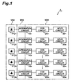
- Fig. 1 is a schematic view of a photodetector 1 of an embodiment.
- This photodetector 1 is equipped with N photodiodes PD 1 to PD N , N integrating circuits 10 1 to 10 N , N CDS (Correlated Double Sampling) circuits 20 1 to 20 N , and N hold circuits 30 1 to 30 N .
- N is an integer of no less than 2.
- Each photodiode PD n generates charges of an amount that is in accordance with the intensity of incident light.
- n is an integer no less than 1 and no more than N.
- Each integrating circuit 10 n inputs the charges generated by photodiode PD n , accumulates these charges in a capacitor, and outputs a voltage that is in accordance with the amount of accumulated charges.
- Each CDS circuit 20 n inputs the voltage output from integrating circuit 10 n and outputs a voltage expressing the variation amount of the input voltage within a fixed time.
- Each hold circuit 30 n inputs the voltage output from CDS circuit 20 n , holds this voltage for a fixed period and outputs this voltage.
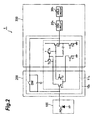
- Fig. 2 is a detailed circuit diagram of an integrating circuit 10 n of photodetector 1 of the present embodiment.
- an anode terminal is grounded and a cathode terminal is connected to an input end of an amplifier 11 n of integrating circuit 10 n .
- Integrating circuit 10 n includes amplifier 11 n , a capacitor C, and a switch SW. Capacitor C and switch SW are mutually connected in parallel and are disposed between the input end and output end of amplifier 11 n .
- a CDS circuit 20 n is connected to the output end of amplifier 11 n . With this integrating circuit 10 n , with the closing of switch SW, capacitor C is discharged and the output voltage is initialized.
- Amplifier 11 n has FET type transistors T 1 to T 7 .
- transistors T 1 , T 2 , T 6 , and T 7 are NMOS transistors, and transistors T 3 , T 4 , and T 5 are PMOS transistors.
- the gate terminal of transistor T 1 is connected to the input end of amplifier 11 n .
- the source terminal of transistor T 1 and the source terminal of transistor T 2 are respectively connected to the drain terminal of transistor T 7 .
- the source terminal of transistor T 7 is grounded.
- the drain terminal of transistor T 1 is connected to the gate terminal and the drain terminal of transistor T 3 and the gate terminal of transistor T 4 .
- the drain terminal of transistor T 2 is connected to the drain terminal of transistor T 4 and the gate terminal of transistor T 5 .
- the drain terminal of transistor T 5 is connected to the drain terminal of transistor T 6 and to the output end of amplifier 11 n .
- the source terminal of transistor T 6 is grounded.
- a predetermined voltage is input into the source terminal of each of transistors T 3 to T 5 .
- a predetermined DC voltage is input into the gate terminal of each of transistors T 2 , T 6 , and T 7 .
- a capacitor and a resistor element are connected in series between the drain and the gate of transistor T 5 as shown in Fig. 2.
- transistors T 1 to T 7 transistors T 1 and T 2 at the input end side form a differential pair input part of amplifier 11 n . Also, transistors T 5 and T 6 at the output end side form a drive part of amplifier 11 n . Whereas the amount of heat generated by the differential pair input part is comparatively low, the amount of heat generated by the drive part is comparatively high.
- photodetector 1 of the present embodiment is divided among the three substrates of a first substrate 100, a second substrate 200, and a third substrate 300. That is, the N photodiodes PD 1 to PD N are aligned one-dimensionally or two-dimensionally on first substrate 100. On second substrate 200 are positioned the differential pair input part of amplifier 11 n , capacitor C, and switch SW of each of the N integrating circuits 10 1 to 10 N .
- On third substrate 300 are positioned the drive part and the other transistors T 3 , T 4 , and T 7 of amplifier 11 n of each of the N integrating circuits 10 1 to 10 N , as well as the N CDS circuits 20 1 to 20 N and the N hold circuits 30 1 to 30 N .
- Fig. 3 is a perspective view showing the positional relationship of first substrate 100, second substrate 200, and third substrate 300 of photodetector 1 of the present embodiment.
- substrates 100 and 200 are electrically connected to each other and substrates 200 and 300 are electrically connected to each other through bump electrodes.
- the respective substrates are mounted so as to overlap in the direction of incidence of light, and first substrate 100 and second substrate 200 are bump-connected to each other and second substrate 200 and third substrate 300 are bump-connected to each other.
- a voltage expressing the variation amount over a fixed time of the voltage output from integrating circuit 10 n is then output from CDS circuit 20 n , disposed on third substrate 300, and the voltage output from CDS circuit 20 n is then held for a fixed period and then output by hold circuit 30 n , disposed on third substrate 300.
- Fig. 4 is a diagram showing an example of a cross section of first substrate 100 and second substrate 200 of photodetector 1 of the present embodiment. Since in Fig.4, a basic pattern is repeated in the left and right directions, the following description shall concern only a single basic pattern.
- first substrate 100 on a first surface (the upper side surface in Fig.4) of an n-type semiconductor substrate are formed a p + region 111, which forms a pn junction with the n-type substrate and thereby makes up a photodiode PD, and an n + region 112, which serves as an isolation region. Also, with first substrate 100, on a second surface (the lower side surface in Fig.
- first substrate 100 has a through hole 131, passing through between the first surface and the second surface, and a through electrode 131 is disposed in this through hole.
- a metal wiring layer 113 which electrically connects p + region 111 and through electrode 131, is formed on the first surface side of first substrate 100, and a metal electrode 123, which is electrically connected with through electrode 131, is formed on the second surface side.
- a metal electrode 223, which is electrically connected to the input end of an integrating circuit 10 n , and a metal electrode 224, which is electrically connected to a ground potential, are formed on a first surface (the upper side surface in Fig.4) of a semiconductor substrate.
- Metal electrode 123 of first substrate 100 and metal electrode 223 of second substrate 200 are connected to each other by a bump 423, and metal electrode 124 of first substrate 100 and metal electrode 224 of second substrate 200 are connected to each other by a bump 424.
- the gap between first substrate 100 and second substrate is filled with a resin.
- first substrate 100 On the first surface side of first substrate 100 are positioned a scintillator 510 and a shielding member 520.
- Scintillator 510 is disposed above p + region 111 of first substrate 100 and generates scintillation light upon incidence of X-rays or other energy rays.
- Shielding material 520 is disposed above n + region 112 of first substrate 100, blocks the transmission of X-rays and other energy rays, and fixes scintillator 510.
- Fig. 5 is a diagram showing another example of a cross section of first substrate 100 and second substrate 200 of photodetector 1 of the present embodiment. Since a basic pattern is repeated in the left and right directions in Fig. 5 as well, the following description shall concern only a single basic pattern.
- first substrate 100 On a first surface (the upper side surface in the Fig.5) of an n-type semiconductor substrate are formed an n + -type accumulation layer 151 for preventing charge recombination and an insulating protective layer 152 for protecting the surface.
- first substrate 100 on a second surface (the lower side surface in the Fig.5) of the n-type semiconductor substrate are formed a p + region 161, which forms a pn junction with the n-type substrate and thereby makes up a photodiode PD, and an n + region 162, which serves as an isolation region, and a protective layer 163 is formed above these regions.
- a metal electrode 164 Also on the second surface of first substrate 100 are formed a metal electrode 164, which is electrically connected with p + region 161, and a metal electrode 165, which is electrically connected with n + region 162.
- Metal electrode 164 of first substrate 100 and metal electrode 264 of second substrate 200 are connected to each other by a bump 464, and metal electrode 165 of first substrate 100 and metal electrode 265 of second substrate 200 are connected to each other by a bump 465.
- the gap between first substrate 100 and second substrate is filled with a resin.
- first substrate 100 On the first surface of first substrate 100 are positioned a scintillator 510 and a shielding member 520.
- Scintillator 510 is disposed above p + region 161 of first substrate 100 and generates scintillation light upon incidence of X-rays or other energy rays.
- Shielding material 520 is disposed above n + region 162 of first substrate 100, blocks the transmission of X-rays and other energy rays, and fixes scintillator 510.
- the first surface side is made thin in thickness by chemical-mechanical polishing, anisotropic etching, etc.
- the wiring on first substrate 100 can thus be lessened in amount or shortened to enable an increased number of pixels and high density to be realized readily on the first substrate. Also, since the charge transfer path from photodiode PD n on first substrate 100 to the differential pair input part of amplifier 11 n and capacitor C of integrating circuit 10 n on second substrate 200 can be shortened, the superposition of noise is restrained, and accurate photodetection is thereby enabled.
- each integrating circuit 10 n on third substrate 300 is high in heat generation amount, since it is disposed away from first substrate 100, on which each photodiode PD n is formed, temperature rise of each photodiode PD n on first substrate 100 is restrained and accurate photodetection is enabled from this point as well.
- This embodiment is also favorable in that optimal manufacturing processes can be employed for first substrate 100, on which a photodiode array is formed, and for second substrate 200 and third substrate 300, on which signal processing circuits, such as the integrating circuits, are formed.
- Fig. 6 is a perspective view showing the positional relationship of a first substrate 100 and a second substrate 210 of a photodetector 2 of another embodiment.
- First substrate 100 of this photodetector 2 is the same in arrangement as first substrate 100 of the above-described photodetector 1 and has N photodiodes PD 1 to PD n formed thereon.
- second substrate 210 is substantially the same as an arrangement in which second substrate 200 and third substrate 300 of the above-described photodetector 1 are put together.
- Second substrate 210 of this photodetector 2 includes a first region 211 and a second region 212.
- First region 211 of second substrate 210 is connected by a bump B to first substrate 100, thereby electrically connecting a photodiode PD n and the input end of an integrating circuit 10 n to each other.
- First region 211 of second substrate 210 is a region that overlaps with a region on first substrate 100 on which photodiodes PD 1 to PD N are disposed and, as with second substrate 200 of the above-described photodetector 1, has capacitor C and the differential pair input part of amplifier 11 n of integrating circuit 10 n disposed therein.
- second region 212 of second substrate 210 is a region that does not overlap with the region on first substrate 100 on which photodiodes PD 1 to PD N are disposed and, as with third substrate 300 of the above-described photodetector 1, has the drive part of amplifier 11 n of integrating circuit 10 n disposed therein.
- the amplifier included in the integrating circuit is not limited to that of the arrangement shown in Fig. 2 and may be of another arrangement.
- the respective cross-sectional structures of first substrate 100 and second substrate 200 are not restricted to those shown in each of Figs. 4 and 5.
- another circuit for example, an A/D conversion circuit, etc., may be disposed on third substrate 300 or in second region 212 of second substrate 210.
- the differential pair input parts of amplifiers and capacitors of integrating circuits are disposed on a second substrate (or in a first region of a second substrate), which is connected by bumps to a first substrate.
- the drive parts of the amplifier of the integrating circuits are disposed on a third substrate (or in a second region of the second substrate), which is not bump-connected to the first substrate.
- This invention can be used in a photodetector.
Landscapes
- Physics & Mathematics (AREA)
- General Physics & Mathematics (AREA)
- Spectroscopy & Molecular Physics (AREA)
- Engineering & Computer Science (AREA)
- Multimedia (AREA)
- Signal Processing (AREA)
- Solid State Image Pick-Up Elements (AREA)
- Measurement Of Radiation (AREA)
- Photometry And Measurement Of Optical Pulse Characteristics (AREA)
- Light Receiving Elements (AREA)
- Transforming Light Signals Into Electric Signals (AREA)
Abstract
Description
Claims (3)
- A photodetector comprising:a plurality of photodiodes, each generating charges of an amount that is in accordance with the intensity of incident light; andintegrating circuits, each including an amplifier, having a differential pair input part at the input end side and a drive part at the output end side, and a capacitor and a switch, which are disposed between said input end and said output end of said amplifier, and, when said switch is opened, accumulating, in the capacitor, charges input into said input end from an above-mentioned photodiode and outputting, from said output end, a voltage that is in accordance with the amount of charges accumulated in said capacitor,said plurality of photodiodes being disposed on a first substrate,said capacitors and said differential pair input parts being disposed on a second substrate,said drive parts being disposed on a third substrate, andsaid photodiodes and said input ends of said integrating circuits being electrically connected to each other by said first substrate and said second substrate being bump-connected to each other.
- The photodetector according to Claim 1, wherein said second substrate and said third substrate are bump-connected to each other.
- A photodetector comprising:a plurality of photodiodes, each generating charges of an amount that is in accordance with the intensity of incident light; andintegrating circuits, each including an amplifier, having a differential pair input part at the input end side and a drive part at the output end side, and a capacitor and a switch, which are disposed between said input end and said output end of said amplifier, and, when said switch is opened, accumulating, in the capacitor, charges input into said input end from an above-mentioned photodiode and outputting, from said output end, a voltage that is in accordance with the amount of charges accumulated in said capacitor,said plurality of photodiodes being disposed on a first substrate,said capacitors, said differential pair input parts, and said drive parts being disposed .on a second substrate,said photodiodes and said input ends of the integrating circuits being electrically connected to each other by said first substrate and said second substrate being bump-connected to each other,said capacitors and said differential pair input parts being disposed in a first region on said second substrate that overlaps with a region on said first substrate in which said plurality of photodiodes are disposed, andsaid drive parts are disposed in a second region on said second substrate that does not overlap with the region on said first substrate in which said plurality of photodiodes are disposed.
Applications Claiming Priority (3)
| Application Number | Priority Date | Filing Date | Title |
|---|---|---|---|
| JP2002034298 | 2002-02-12 | ||
| JP2002034298A JP4012743B2 (en) | 2002-02-12 | 2002-02-12 | Photodetector |
| PCT/JP2003/001444 WO2003069288A1 (en) | 2002-02-12 | 2003-02-12 | Optical sensor |
Publications (3)
| Publication Number | Publication Date |
|---|---|
| EP1473553A1 true EP1473553A1 (en) | 2004-11-03 |
| EP1473553A4 EP1473553A4 (en) | 2007-03-21 |
| EP1473553B1 EP1473553B1 (en) | 2017-12-13 |
Family
ID=27678025
Family Applications (1)
| Application Number | Title | Priority Date | Filing Date |
|---|---|---|---|
| EP03703333.9A Expired - Lifetime EP1473553B1 (en) | 2002-02-12 | 2003-02-12 | Stacked optical sensor |
Country Status (7)
| Country | Link |
|---|---|
| US (1) | US7336808B2 (en) |
| EP (1) | EP1473553B1 (en) |
| JP (1) | JP4012743B2 (en) |
| CN (1) | CN100432641C (en) |
| AU (1) | AU2003207058A1 (en) |
| IL (1) | IL163454A (en) |
| WO (1) | WO2003069288A1 (en) |
Cited By (6)
| Publication number | Priority date | Publication date | Assignee | Title |
|---|---|---|---|---|
| US7170143B2 (en) | 2003-10-20 | 2007-01-30 | Hamamatsu Photonics K.K. | Semiconductor photo-detection device and radiation apparatus |
| EP1554760B1 (en) * | 2002-10-25 | 2009-08-19 | Ipl Intellectual Property Licensing Limited | Circuit substrate and method |
| US8084836B2 (en) | 2006-12-21 | 2011-12-27 | Hamamatsu Photonics K.K. | Semiconductor photodetector and radiation detecting apparatus |
| DE102011081100A1 (en) * | 2011-08-17 | 2013-02-21 | Siemens Aktiengesellschaft | Arrangement with photocells |
| WO2014072203A1 (en) | 2012-11-09 | 2014-05-15 | Siemens Aktiengesellschaft | Photoreceiver with a plurality of photocells and through-hole contacts, and method for the production thereof |
| US10559619B2 (en) | 2016-02-22 | 2020-02-11 | Sony Corporation | Imaging device and method of manufacturing imaging device |
Families Citing this family (27)
| Publication number | Priority date | Publication date | Assignee | Title |
|---|---|---|---|---|
| JP4589030B2 (en) * | 2004-05-10 | 2010-12-01 | 浜松ホトニクス株式会社 | Photodetector |
| US20060045383A1 (en) * | 2004-08-31 | 2006-03-02 | Picciotto Carl E | Displacement estimation system and method |
| TW201101476A (en) | 2005-06-02 | 2011-01-01 | Sony Corp | Semiconductor image sensor module and method of manufacturing the same |
| CN101233394B (en) * | 2005-07-27 | 2014-02-26 | 株式会社半导体能源研究所 | Semiconductor device |
| KR100798276B1 (en) * | 2006-08-23 | 2008-01-24 | 동부일렉트로닉스 주식회사 | Image sensor and its manufacturing method |
| KR100860466B1 (en) * | 2006-12-27 | 2008-09-25 | 동부일렉트로닉스 주식회사 | CMOS image sensor and manufacturing method |
| JP2009158570A (en) * | 2007-12-25 | 2009-07-16 | Seiko Instruments Inc | Photodetection semiconductor device, photodetection device, and image display device |
| KR100856942B1 (en) * | 2008-01-07 | 2008-09-04 | 주식회사 동부하이텍 | Image sensor and manufacturing method |
| JP5256862B2 (en) * | 2008-06-06 | 2013-08-07 | 富士通株式会社 | Imaging device |
| JP5185205B2 (en) | 2009-02-24 | 2013-04-17 | 浜松ホトニクス株式会社 | Semiconductor photo detector |
| JP5185207B2 (en) | 2009-02-24 | 2013-04-17 | 浜松ホトニクス株式会社 | Photodiode array |
| JP5185206B2 (en) | 2009-02-24 | 2013-04-17 | 浜松ホトニクス株式会社 | Semiconductor photo detector |
| JP5185208B2 (en) | 2009-02-24 | 2013-04-17 | 浜松ホトニクス株式会社 | Photodiode and photodiode array |
| JP2010283223A (en) * | 2009-06-05 | 2010-12-16 | Hamamatsu Photonics Kk | Semiconductor light detection element and method for manufacturing semiconductor light detection element |
| JP5363222B2 (en) * | 2009-07-13 | 2013-12-11 | 浜松ホトニクス株式会社 | Semiconductor light detection element and method for manufacturing semiconductor light detection element |
| JP5261304B2 (en) * | 2009-07-13 | 2013-08-14 | 浜松ホトニクス株式会社 | Semiconductor light detection element and method for manufacturing semiconductor light detection element |
| US8629524B2 (en) | 2012-04-27 | 2014-01-14 | Taiwan Semiconductor Manufacturing Company, Ltd. | Apparatus for vertically integrated backside illuminated image sensors |
| US10090349B2 (en) | 2012-08-09 | 2018-10-02 | Taiwan Semiconductor Manufacturing Company, Ltd. | CMOS image sensor chips with stacked scheme and methods for forming the same |
| US8957358B2 (en) | 2012-04-27 | 2015-02-17 | Taiwan Semiconductor Manufacturing Company, Ltd. | CMOS image sensor chips with stacked scheme and methods for forming the same |
| US9153565B2 (en) | 2012-06-01 | 2015-10-06 | Taiwan Semiconductor Manufacturing Company, Ltd. | Image sensors with a high fill-factor |
| US10297630B2 (en) * | 2012-06-18 | 2019-05-21 | Forza Silicon Corporation | Pinned charge transimpedance amplifier |
| JP5682638B2 (en) * | 2013-01-15 | 2015-03-11 | 株式会社ニコン | Image sensor |
| JP6361633B2 (en) * | 2015-11-02 | 2018-07-25 | 株式会社ニコン | Image sensor |
| KR101699810B1 (en) * | 2016-05-31 | 2017-01-26 | 주식회사 이와이엘 | Quantum random pulse generator |
| JP6779825B2 (en) | 2017-03-30 | 2020-11-04 | キヤノン株式会社 | Semiconductor devices and equipment |
| JP7533533B2 (en) * | 2020-06-16 | 2024-08-14 | 株式会社ニコン | Image sensor |
| FR3120741B1 (en) * | 2021-03-09 | 2023-12-08 | St Microelectronics Alps Sas | Photosensitive device comprising an integrator circuit per group of at least two photosensitive elements. |
Family Cites Families (20)
| Publication number | Priority date | Publication date | Assignee | Title |
|---|---|---|---|---|
| JPH0730030B2 (en) | 1983-08-24 | 1995-04-05 | 日産化学工業株式会社 | Pyrazole sulfonylurea derivative, process for its production and selective herbicide containing said derivative |
| US4843520A (en) | 1987-02-03 | 1989-06-27 | Matsushita Electric Industrial Co. Ltd. | Electronic circuit module |
| JPH077814B2 (en) * | 1987-02-03 | 1995-01-30 | 松下電器産業株式会社 | Mounting board |
| JPS63205527A (en) * | 1987-02-20 | 1988-08-25 | Sanyo Electric Co Ltd | Photometric circuit |
| JPS63298187A (en) * | 1987-05-29 | 1988-12-05 | Matsushita Electric Ind Co Ltd | Radiation sensor array |
| JPH01239915A (en) * | 1988-03-22 | 1989-09-25 | Nec Corp | Semiconductor integrated circuit |
| JPH02271281A (en) | 1989-04-13 | 1990-11-06 | Matsushita Electric Ind Co Ltd | detector unit |
| JP2617798B2 (en) * | 1989-09-22 | 1997-06-04 | 三菱電機株式会社 | Stacked semiconductor device and method of manufacturing the same |
| JP2940726B2 (en) * | 1991-07-02 | 1999-08-25 | 三洋電機株式会社 | Optical semiconductor device |
| JPH0629507A (en) * | 1992-04-21 | 1994-02-04 | Nec Corp | Photodiode provided with operation function |
| US5665959A (en) * | 1995-01-13 | 1997-09-09 | The United States Of America As Represented By The Administrator Of The National Aeronautics And Space Adminstration | Solid-state image sensor with focal-plane digital photon-counting pixel array |
| US6144718A (en) * | 1997-11-26 | 2000-11-07 | General Electric Company | Flexible cable connection for detector module |
| US6552745B1 (en) * | 1998-04-08 | 2003-04-22 | Agilent Technologies, Inc. | CMOS active pixel with memory for imaging sensors |
| JP3668926B2 (en) * | 1999-08-27 | 2005-07-06 | 株式会社ルネサステクノロジ | Optical interconnection receiver module |
| US6525415B2 (en) * | 1999-12-28 | 2003-02-25 | Fuji Xerox Co., Ltd. | Three-dimensional semiconductor integrated circuit apparatus and manufacturing method therefor |
| JP2001291877A (en) * | 2000-04-05 | 2001-10-19 | Hamamatsu Photonics Kk | Solid-state imaging device |
| US6483116B1 (en) * | 2000-04-25 | 2002-11-19 | Innovative Technology Licensing, Llc | High performance ultraviolet imager for operation at room temperature |
| US6476374B1 (en) * | 2000-04-25 | 2002-11-05 | Innovative Technology Licensing, Llc | Room temperature, low-light-level visible imager |
| JP3713418B2 (en) * | 2000-05-30 | 2005-11-09 | 光正 小柳 | Manufacturing method of three-dimensional image processing apparatus |
| JP2002354195A (en) * | 2001-05-29 | 2002-12-06 | Hamamatsu Photonics Kk | Signal processing circuit and solid-state imaging device |
-
2002
- 2002-02-12 JP JP2002034298A patent/JP4012743B2/en not_active Expired - Fee Related
-
2003
- 2003-02-12 CN CNB038036436A patent/CN100432641C/en not_active Expired - Fee Related
- 2003-02-12 US US10/504,267 patent/US7336808B2/en not_active Expired - Fee Related
- 2003-02-12 AU AU2003207058A patent/AU2003207058A1/en not_active Abandoned
- 2003-02-12 EP EP03703333.9A patent/EP1473553B1/en not_active Expired - Lifetime
- 2003-02-12 WO PCT/JP2003/001444 patent/WO2003069288A1/en not_active Ceased
-
2004
- 2004-08-10 IL IL163454A patent/IL163454A/en not_active IP Right Cessation
Cited By (12)
| Publication number | Priority date | Publication date | Assignee | Title |
|---|---|---|---|---|
| EP1554760B1 (en) * | 2002-10-25 | 2009-08-19 | Ipl Intellectual Property Licensing Limited | Circuit substrate and method |
| US7170143B2 (en) | 2003-10-20 | 2007-01-30 | Hamamatsu Photonics K.K. | Semiconductor photo-detection device and radiation apparatus |
| US8592934B2 (en) | 2003-10-20 | 2013-11-26 | Hamamatsu Photonics K.K. | Semiconductor photo-detection device and radiation detection apparatus |
| US9099599B2 (en) | 2003-10-20 | 2015-08-04 | Hamamatsu Photonics K.K. | Semiconductor photo-detection device and radiation detection apparatus |
| US9431567B2 (en) | 2003-10-20 | 2016-08-30 | Hamamatsu Photonics K.K. | Semiconductor photo-detection device and radiation detection apparatus |
| US10908302B2 (en) | 2003-10-20 | 2021-02-02 | Hamamatsu Photonics K.K. | Semiconductor photo-detection device and radiation detection apparatus |
| US8084836B2 (en) | 2006-12-21 | 2011-12-27 | Hamamatsu Photonics K.K. | Semiconductor photodetector and radiation detecting apparatus |
| DE102011081100A1 (en) * | 2011-08-17 | 2013-02-21 | Siemens Aktiengesellschaft | Arrangement with photocells |
| WO2014072203A1 (en) | 2012-11-09 | 2014-05-15 | Siemens Aktiengesellschaft | Photoreceiver with a plurality of photocells and through-hole contacts, and method for the production thereof |
| DE102012220416A1 (en) | 2012-11-09 | 2014-05-15 | Siemens Aktiengesellschaft | Photoreceptor with a plurality of photocells and vias and method for its production |
| US10559619B2 (en) | 2016-02-22 | 2020-02-11 | Sony Corporation | Imaging device and method of manufacturing imaging device |
| US10707256B2 (en) | 2016-02-22 | 2020-07-07 | Sony Corporation | Imaging device and method of manufacturing imaging device |
Also Published As
| Publication number | Publication date |
|---|---|
| EP1473553B1 (en) | 2017-12-13 |
| IL163454A (en) | 2009-06-15 |
| JP2003232679A (en) | 2003-08-22 |
| WO2003069288A1 (en) | 2003-08-21 |
| EP1473553A4 (en) | 2007-03-21 |
| CN1630810A (en) | 2005-06-22 |
| JP4012743B2 (en) | 2007-11-21 |
| US20060165294A1 (en) | 2006-07-27 |
| CN100432641C (en) | 2008-11-12 |
| US7336808B2 (en) | 2008-02-26 |
| AU2003207058A1 (en) | 2003-09-04 |
Similar Documents
| Publication | Publication Date | Title |
|---|---|---|
| US7336808B2 (en) | Optical sensor | |
| KR101511388B1 (en) | Photodetector array and method of operation | |
| JP3645585B2 (en) | Charge coupled device type solid-state imaging device having overflow drain structure | |
| KR101075626B1 (en) | Photo-detection device | |
| CN100499141C (en) | Solid camera device | |
| EP3540390B1 (en) | Light detection device | |
| CN112088435B (en) | Back-illuminated semiconductor light detection device | |
| CN113614931B (en) | Light detector | |
| CN109952649B (en) | Light detection device | |
| WO2004047180A1 (en) | Photo detection device | |
| JP7414791B2 (en) | Photoelectric conversion devices and equipment | |
| CN1897272B (en) | Photoelectric detection system | |
| US8836065B2 (en) | Solid-state imaging device | |
| EP1850387B1 (en) | Solid-state image pickup device | |
| EP3082164B1 (en) | Radiation image sensor | |
| JP7833657B2 (en) | Imaging device and its driving method | |
| WO2022202451A1 (en) | Photodetector and distance measurement system | |
| CN100358152C (en) | Solid-state camera device | |
| CN110970453A (en) | camera | |
| US7045761B2 (en) | Self-pixelating focal plane array with electronic output | |
| US7701026B2 (en) | Imaging device | |
| US20250287125A1 (en) | Semiconductor structure and method of manufacturing the same | |
| KR100299575B1 (en) | Solid-state image sensor | |
| JP4951212B2 (en) | Image sensor | |
| JPH06302799A (en) | Solid-state image sensing device |
Legal Events
| Date | Code | Title | Description |
|---|---|---|---|
| PUAI | Public reference made under article 153(3) epc to a published international application that has entered the european phase |
Free format text: ORIGINAL CODE: 0009012 |
|
| 17P | Request for examination filed |
Effective date: 20040811 |
|
| AK | Designated contracting states |
Kind code of ref document: A1 Designated state(s): AT BE BG CH CY CZ DE DK EE ES FI FR GB GR HU IE IT LI LU MC NL PT SE SI SK TR |
|
| AX | Request for extension of the european patent |
Extension state: AL LT LV MK RO |
|
| A4 | Supplementary search report drawn up and despatched |
Effective date: 20070220 |
|
| RIC1 | Information provided on ipc code assigned before grant |
Ipc: G01J 1/44 20060101AFI20030823BHEP Ipc: H01L 27/14 20060101ALI20070214BHEP Ipc: G01T 1/20 20060101ALI20070214BHEP Ipc: H01L 25/16 20060101ALI20070214BHEP Ipc: G01J 1/02 20060101ALI20070214BHEP Ipc: H01L 31/10 20060101ALI20070214BHEP Ipc: H04N 5/335 20060101ALI20070214BHEP |
|
| 17Q | First examination report despatched |
Effective date: 20070420 |
|
| REG | Reference to a national code |
Ref country code: DE Ref legal event code: R079 Ref document number: 60350841 Country of ref document: DE Free format text: PREVIOUS MAIN CLASS: G01J0001440000 Ipc: H01L0025160000 |
|
| GRAP | Despatch of communication of intention to grant a patent |
Free format text: ORIGINAL CODE: EPIDOSNIGR1 |
|
| RIC1 | Information provided on ipc code assigned before grant |
Ipc: H01L 25/16 20060101AFI20170612BHEP Ipc: H01L 27/146 20060101ALI20170612BHEP Ipc: G01J 1/44 20060101ALI20170612BHEP Ipc: H04N 5/3745 20110101ALI20170612BHEP |
|
| INTG | Intention to grant announced |
Effective date: 20170628 |
|
| GRAS | Grant fee paid |
Free format text: ORIGINAL CODE: EPIDOSNIGR3 |
|
| GRAA | (expected) grant |
Free format text: ORIGINAL CODE: 0009210 |
|
| AK | Designated contracting states |
Kind code of ref document: B1 Designated state(s): DE FR NL |
|
| REG | Reference to a national code |
Ref country code: FR Ref legal event code: PLFP Year of fee payment: 16 |
|
| REG | Reference to a national code |
Ref country code: DE Ref legal event code: R096 Ref document number: 60350841 Country of ref document: DE |
|
| PGFP | Annual fee paid to national office [announced via postgrant information from national office to epo] |
Ref country code: NL Payment date: 20180115 Year of fee payment: 16 |
|
| REG | Reference to a national code |
Ref country code: NL Ref legal event code: MP Effective date: 20171213 |
|
| PGFP | Annual fee paid to national office [announced via postgrant information from national office to epo] |
Ref country code: FR Payment date: 20180111 Year of fee payment: 16 |
|
| PG25 | Lapsed in a contracting state [announced via postgrant information from national office to epo] |
Ref country code: NL Free format text: LAPSE BECAUSE OF FAILURE TO SUBMIT A TRANSLATION OF THE DESCRIPTION OR TO PAY THE FEE WITHIN THE PRESCRIBED TIME-LIMIT Effective date: 20171213 |
|
| REG | Reference to a national code |
Ref country code: DE Ref legal event code: R119 Ref document number: 60350841 Country of ref document: DE |
|
| PLBE | No opposition filed within time limit |
Free format text: ORIGINAL CODE: 0009261 |
|
| STAA | Information on the status of an ep patent application or granted ep patent |
Free format text: STATUS: NO OPPOSITION FILED WITHIN TIME LIMIT |
|
| 26N | No opposition filed |
Effective date: 20180914 |
|
| PG25 | Lapsed in a contracting state [announced via postgrant information from national office to epo] |
Ref country code: DE Free format text: LAPSE BECAUSE OF NON-PAYMENT OF DUE FEES Effective date: 20180901 |
|
| PG25 | Lapsed in a contracting state [announced via postgrant information from national office to epo] |
Ref country code: FR Free format text: LAPSE BECAUSE OF NON-PAYMENT OF DUE FEES Effective date: 20190228 |