EP1469600A1 - Nonlinear resistor circuit using floating gate mosfets - Google Patents

Nonlinear resistor circuit using floating gate mosfets Download PDF

Info

Publication number
EP1469600A1
EP1469600A1 EP03701832A EP03701832A EP1469600A1 EP 1469600 A1 EP1469600 A1 EP 1469600A1 EP 03701832 A EP03701832 A EP 03701832A EP 03701832 A EP03701832 A EP 03701832A EP 1469600 A1 EP1469600 A1 EP 1469600A1
Authority
EP
European Patent Office
Prior art keywords
nonlinear resistor
resistor circuit
voltage
shaped
characteristic
Prior art date
Legal status (The legal status is an assumption and is not a legal conclusion. Google has not performed a legal analysis and makes no representation as to the accuracy of the status listed.)
Granted
Application number
EP03701832A
Other languages
German (de)
French (fr)
Other versions
EP1469600A4 (en
EP1469600B1 (en
Inventor
Yoshihiko Horio
Tetsuya Fujiwara
Kazuyuki Aihara
Current Assignee (The listed assignees may be inaccurate. Google has not performed a legal analysis and makes no representation or warranty as to the accuracy of the list.)
Japan Science and Technology Agency
Original Assignee
Japan Science and Technology Agency
Priority date (The priority date is an assumption and is not a legal conclusion. Google has not performed a legal analysis and makes no representation as to the accuracy of the date listed.)
Filing date
Publication date
Application filed by Japan Science and Technology Agency filed Critical Japan Science and Technology Agency
Publication of EP1469600A1 publication Critical patent/EP1469600A1/en
Publication of EP1469600A4 publication Critical patent/EP1469600A4/en
Application granted granted Critical
Publication of EP1469600B1 publication Critical patent/EP1469600B1/en
Anticipated expiration legal-status Critical
Expired - Lifetime legal-status Critical Current

Links

Images

Classifications

    • HELECTRICITY
    • H03ELECTRONIC CIRCUITRY
    • H03HIMPEDANCE NETWORKS, e.g. RESONANT CIRCUITS; RESONATORS
    • H03H11/00Networks using active elements
    • H03H11/46One-port networks
    • H03H11/53One-port networks simulating resistances; simulating resistance multipliers
    • HELECTRICITY
    • H03ELECTRONIC CIRCUITRY
    • H03HIMPEDANCE NETWORKS, e.g. RESONANT CIRCUITS; RESONATORS
    • H03H11/00Networks using active elements
    • H03H11/46One-port networks
    • H03H11/52One-port networks simulating negative resistances

Definitions

  • the present invention relates to a nonlinear resistor circuit using floating gate MOSFETs, and more particularly, to a circuit which realizes various N-shaped voltage-current characteristics.
  • the inventor of the.present invention suggests a conventional nonlinear resistor circuit using the multi-input floating gate MOSFET as one of circuits having a negative voltage-current (V-I) characteristic area (in reference document (1)), and it is applied to an inductor simulation or a sine wave oscillator circuit (in reference documents (2) to (4)).
  • V-I negative voltage-current
  • an N-shaped nonlinear resistor characteristic has the negative resistor area in the center and therefore is widely used for an oscillating circuit or neuron device.
  • the N-shaped nonlinear resistor characteristic approximates to the piecewise linear characteristics of third to fifth orders can form a sine wave oscillator or a chaos generating circuit by combining L and C (in reference documents (5) and (6)).
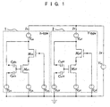
  • Fig. 1 is a diagram showing an N-shaped nonlinear resistor circuit using floating gate MOSFETs according to the present invention.
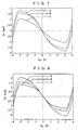
  • Fig. 2 are diagrams (numerical simulations) showing various V xy -I A characteristics in Fig. 1, Fig. 2(a) is a diagram showing the characteristic with a voltage. V xA as a parameter, Fig. 2(b) is a diagram showing the characteristic with a voltage V yA as a parameter, Fig. 2(c) is a diagram showing the characteristic with a voltage V nA as a parameter, and Fig. 2(d) is a diagram showing the characteristic with a voltage V pA , as a parameter.
  • Fig. 1 is a diagram showing an N-shaped nonlinear resistor circuit using floating gate MOSFETs according to the present invention.
  • Fig. 2 are diagrams (numerical simulations) showing various V xy -I A characteristics in Fig. 1
  • Fig. 2(a) is
  • FIG. 3 are diagrams (numerical simulations) showing various V xy -I V characteristics in Fig. 1, Fig. 3(a) is a diagram showing the characteristic with a voltage V xV as a parameter, Fig. 3(b) is a diagram showing the characteristic with a voltage V yV as a parameter, Fig. 3(c) is a diagram showing the characteristic with a voltage V nV as a parameter, and Fig. 3(d) is a diagram showing the characteristic with a voltage V pV as a parameter.
  • the circuit is formed by connecting in parallel a ⁇ -shaped nonlinear resistor circuit 1 and a V-shaped nonlinear resistor circuit 2 using multi-input floating gate MOSFETs (refer to reference document (1)).
  • Figs. 2 and 3 show the nonlinear resistor characteristics of the currents I A and I V , respectively, in Fig. 1 for the voltage V xy .
  • capacitors C p2A and C p1A are connected to a gate terminal of a normal P-channel MOSFET and they are set as input terminals. Inputs are applied via the capacitors C p2A and C p1A , thereby equivalently setting the gate terminal of the P-channel MOSFET M pA floating.
  • An N-channel MOSFET M nA is serially connected to the P-channel MOSFET M pA .
  • V-shaped nonlinear resistor circuit 2 will be described.
  • capacitors C n1V and C n2V are connected to a gate terminal of a normal N-channel MOSFET and they are set as input terminals. Inputs are applied via the capacitors C n1V and C n2V , thereby equivalently setting the gate terminal of the N-channel MOSFET M nV floating.
  • a P-channel MOSFET M pV is serially connected to the N-channel MOSFET M nV .
  • Fig. 4 are diagrams showing V-I characteristics approximate to a piecewise linearity according to the present invention.
  • Fig. 4(a) shows the characteristic of the third order
  • Fig. 4(b) shows the characteristic of the fourth order
  • Fig. 4(c) shows the characteristic of the fifth order
  • Fig. 4(d) shows the characteristic of the sixth order
  • Fig. 4(e) shows the characteristic of the seventh order.
  • V xy -I N characteristics obtained in Fig. 1 continuously change.
  • these characteristics are approximate to the characteristics of the piecewise linear functions of the third to seventh orders as shown in Fig. 4 and they are described.
  • the number of piecewise linear sections is called an order.
  • the end point in the piecewise linear section is called a break point.
  • the characteristic of the third order shown in Fig. 4(a) is obtained by moving in parallel in the left and right directions the V xy -I A and V xy -I V characteristics shown in Figs. 2 and 3 by the voltage V xA or V yA and the voltage V xV or V yV shown in Fig. 1.
  • the center portion of the V xy -I N characteristic may entirely be one linear piecewise.
  • the negative portions of the ⁇ -shaped and V-shaped characteristics may be linear as much as possible. That is, the setting of V nA , V pA , V nV , and V pV is important. This state is shown in Fig. 5.
  • the fourth to seventh characteristics are realized. These characteristics are different from the characteristics of the third order and the break point is necessary for the center portion of the characteristics. This is realized by adjusting the voltage V pA and V nV in Fig. 1.
  • the fourth order characteristic is realized by adjusting the inclination of the negative portion of the V xy -I A or V xy -I V characteristic.
  • the fifth order characteristic is realized by simultaneously adjusting both the ⁇ -shaped and V-shaped characteristics.
  • the sixth order characteristic is realized by moving in parallel in the lateral axis direction the ⁇ -shaped and V-shaped characteristics used for the fourth order characteristic by the voltage V xA , or V yA and the voltage V xV or V yV in Fig. 1.
  • the seventh order characteristic is obtained by the same method based on the fifth order characteristic.
  • the inclination of the piecewise linear function and the break points may be changed. This will be described in detail with the characteristics of the third and fifth orders that are usually used.
  • the voltages V BP- and V BP+ are determined by the voltages V xA or V yA and the voltage V xV or V yv .
  • the break points B P- and B P+ are enlarged or reduced in the voltage axis direction mainly by the voltages V nA and V pV, thus to shift the break points.
  • the break points are changed while fixing the inclinations m 0 and m 1 as follows.
  • the break point B P1- or B P1+ is changed by enlarging the characteristics of the voltages V nA and V pV in the longitudinal axis direction and changing the length of the piecewise linear portion of the inclination m 1 .
  • the break point B P2- or B P2+ is adjusted by enlarging or reducing the break point H P2- or B P2+ in the voltage-axis direction and in the current-axis direction by the voltage V pA , V xA , or V yA and the voltage V nV , V xV, or V yV. In this case, the fine adjustment with other control voltages is necessary.
  • the N-shaped nonlinear resistor characteristics of the third to seventh orders are confirmed by computer simulations using the V-I characteristic formula using the simple MOSFET-model derived from reference document (1). Particularly, with the characteristics of the third to fifth orders, the adjusting states of the break points and inclinations are indicated in detail.
  • the characteristic approximates to the third order piecewise linearity is shown in the case of using the voltage values in Table 1.
  • a characteristic A has the same inclination m 0 with a characteristic C in Fig. 6 and the break point of the characteristic A is different from the characteristic C.
  • a characteristic B has the same currents I P1- and T P1+ as those of the characteristic C and the inclination m 0 of the characteristic B is different from that of the characteristic C.
  • the break points B P- and B P+ and the inclination m 0 shown in Fig. 4 are changed.
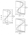
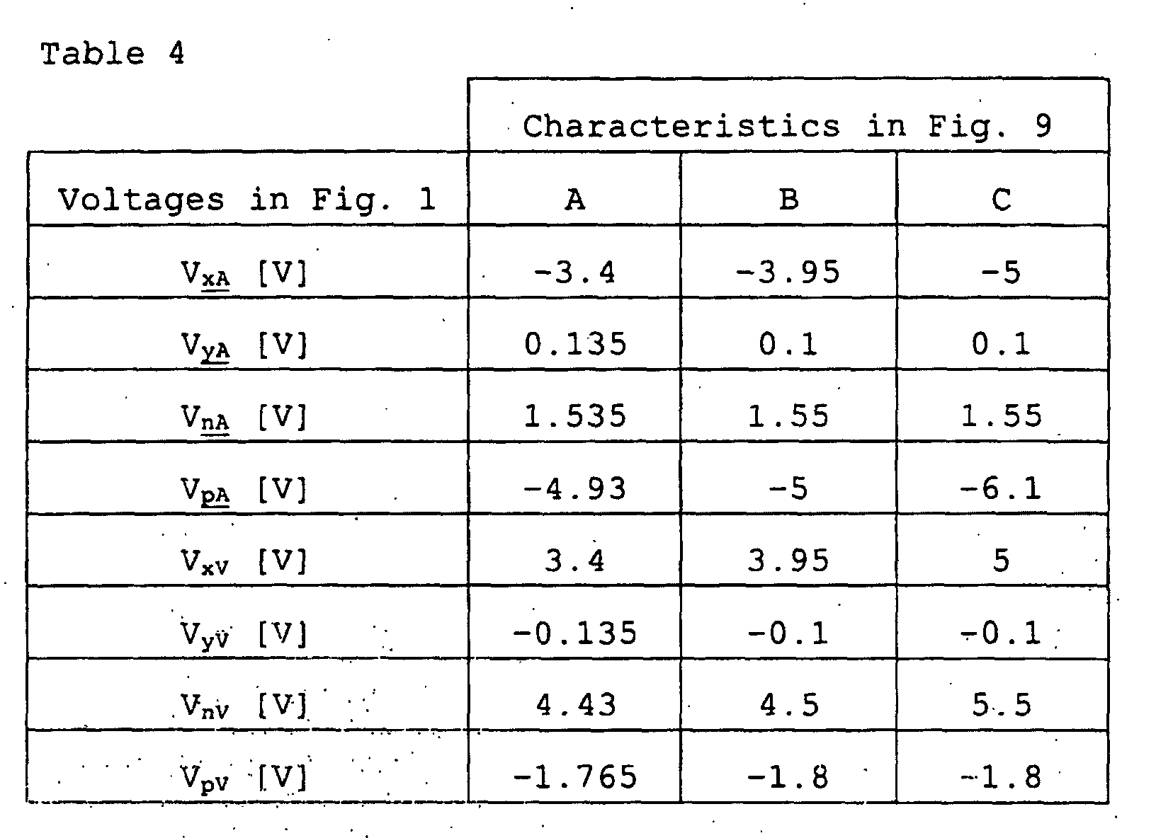
  • V xy -I N characteristic approximates to the fifth order piecewise linear characteristic obtained by the simulation are shown in Figs. 7, 8, and 9. Further, values of control voltages for the characteristics in Figs. 7, 8, and 9 are shown in Tables 2 to 4.
  • Curves B and C in Fig. 7 are shown as examples by changing the inclination m 0 with the fixing of the voltage coordinates of the four break points in Fig. 4(c).
  • curves A and B are shown by changing the inclination m 1 as examples.
  • the voltages V pA and V nV may be changed while keeping the voltages V nA and V pV constant in the case of adjusting the inclination m 0 .
  • the inclination m 1 may be adjusted by coarsely determining the characteristic with the voltages V yA and V yV , and by using the voltages V pA and V nV for fine tuning.
  • Fig. 8 and Table 3 show an example of adjusting the break points B P1- and B P1+ while fixing the inclinations m 0 and m 1 in Fig. 4(c).
  • Fig. 9 and Table 4 show an example of adjusting the break points B P2- and B P2+ .
  • the break points B P1+ and B P1- are determined depending on the voltages V pV and V nA , respectively.
  • the break points B P2+ and B P2- are determined depending on the voltages V xV and V nV and the voltages V xA and V pA , respectively.
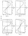
  • Fig. 10 shows the fourth order nonlinear resistor characteristic
  • Fig. 11 shows the sixth order nonlinear resistor characteristic
  • Fig. 12 shows the seventh order nonlinear resistor characteristic.
  • the voltages in Fig. 1 used for the characteristics are shown in Tables 5 to 7. Voltages in Fig. 1 V xA [V] -5.5 V yA [V] 0.1 V nA [V] 1.55 V pA [V] -5.4 V xV [V] 5.5 V yV [V] -0.1 V nV [V] 4.9 V pV [V] -1.8
  • the fourth order characteristic is obtained by changing the voltages V nA , V pA , V nV , and V pV based on the characteristic of the third order.
  • the sixth and seventh order characteristics are obtained by changing the voltages V xA and V xV based on the fourth and fifth order characteristics, respectively.
  • CMOS process parameters of MOSIS TSMC 0.35 ⁇ m CMOS process is used, and the sizes of M nA and M nV in Fig. 1 have W of 20 ⁇ m and L of 0.4 ⁇ m. Further, the sizes of M pA and M pV in Fig. 1 have W of 60 ⁇ m and L of 0.4 ⁇ m.
  • the N-shaped nonlinear resistor circuit is provided with the multi-input floating gate MOSFETs. Further, the numeral calculations and the HSPICE simulations are used to show examples of the V-I characteristics. Further, a method for realizing the characteristics is qualitatively described.
  • the circuit in Fig. 15 comprises discrete parts, and the V xy -I N characteristic is measured.
  • the circuit is shown in Fig. 15.
  • M nA 11 and M nV 12 use 2SK612 and M pA 13 and M pV 14 use 2SJ133.
  • experimental results are shown in Figs. 16 to 20 when capacitances C p1A 15, C p2A 16, C n1V 17, and C n2V 18 are 0.1 ⁇ F.
  • the voltage values in Fig. 15 for realizing the characteristics are shown in Tables 8 to 12.
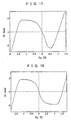
  • Fig. 16 shows the experimental results using the discrete parts of the V xy -I N characteristic of the third order
  • voltage values in Fig. 15 are V A of -0.7V, V nA of 1.55V, V pA of -4.69V, V V of 0.7V, V nV of 3.23V, and V pV of -2.32V as shown in Table 8.
  • Voltages in Fig. 15 V A [V] -0.7 V nA [V] 1.55 V pA [V] -4.69 V V [V] 0.7 V nV [V] 3.23 V pV [V] -2.32
  • Fig. 17 shows the experimental results using the discrete parts of the fourth order V xy -I N characteristic
  • voltage values in Fig. 15 are V A of -1.6V, V nA of 1.46V, V pA , of -5.65V, V V of 1V, V nV of 3.43V, and V pV of -2.28V as shown in Table 9.
  • Voltages in Fig. 15 V A [V] -1.6 V nA [V] 1.46 V pA [V] -5.65 V V [V] 1 V nV [V] 3.43 V pV [V] -2.28
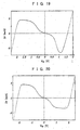
  • Fig. 18 shows the experimental results using the discrete parts of the fifth order V xy -I N characteristic, and voltage values in Fig. 15 are V A of -1.5V; V nA of 1.46V, V pA of -5.65V, V V of 1.5V, V nV of 4.23V, and V pV of -2.18V as shown in Table 10. Voltages in Fig. 15 V A [V] -1.5 V nA [V] 1.46 V pA [V] -5.65 V V [V] 1.5 V nV [V] 4.23 V pV [V] -2.18
  • Fig. 19 shows the experimental results using the discrete parts of the sixth order V xy -I N characteristic
  • voltage values in Fig. 15 are V A of -2.1V, V nA of 1.46V, V pA of -5. 65V, V V of 1. 6V, V nV of 3.43V, and V pV of -2.28V as shown in Table 11.
  • Voltages in Fig. 15 V A [V] -2.1 V nA [V] 1.46 V pA [V] -5.65 V V [V] 1.6 V nV [V] 3.43 V pV [V] -2.28
  • Fig. 20 shows the experimental results using the discrete parts of the seventh order V xy -I N characteristic
  • voltage values in Fig. 15 are V A of -2.1V, V nA of 1.46V, V pA of -5.65V, V V of 2.1V, V nV of 4.23V, and V pV of -2.18V as shown in Table 12.
  • Voltages in Fig. 15 V A [V] -2.1 V nA [V] 1.46 V pA [V] -5.65 V V [V] 2.1 V nV [V] 4.23 V pV [V] -2.18
  • a resistor R(19) is inserted between nodes A and B (on the power supply side of the above-mentioned nonlinear resistor circuit) in Fig. 15, the voltage drop is amplified by an instrumentation amplifier (INA114) 20, and the current IN is obtained based on the amplified output voltages by the following formulae (4) to (6).
  • reference symbol R G denotes resistance for determining gain G of the instrumentation amplifier 20, and R G is 10 k ⁇ . Further, the resistance R is 33 ⁇ and output resistance R o is 10 k ⁇ .
  • I N V o /G ⁇ R
  • the circuit shown in Fig. 15 is an integrated circuit fabricated through MOSIS TSMC 0.35 ⁇ m CMOS semiconductor process.
  • the V xy -I N characteristic measuring circuit comprising the resistor 19 and the measuring amplifier shown in Fig. 15 is not integrated and is mounted outside of the chip by discrete parts.
  • Fig. 21 shows a micro-photograph of the IC chip including the circuit shown in Fig. 15.
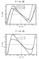
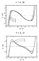
  • Figs. 22 to 28 show the V xy -I N characteristics which are measured from the chip.
  • the voltage values in Fig. 15 for realizing the characteristics are shown in Tables 13 to 19.
  • the characteristics correspond to the simulation characteristics of the third to seventh orders and the HSPICE simulation characteristics.
  • the current IN is obtained by the calculating formulae (4), (5), and (6), similarly to the experiment using discrete parts.
  • the resistances in the calculating formulae (4), (5), and (6) are R G of 240 k ⁇ , R of 10 ⁇ , and output resistance R o of 10 k ⁇ .
  • Voltages in Fig. 15 V A [V] -1.65 V nA [V] 0.65 V pA [V] -8.86 V V [V] 1.65 V nV [V] 7.79 V pV [V] -0.81
  • Another embodiment may be realized by moving in parallel the ⁇ -shaped and V-shaped characteristics in lateral axis direction by the following in Fig. 1.
  • control voltages in the circuit are adjusted, thereby obtaining various V-I characteristics that can be approximated to the piecewise linear functions of the third to seventh orders. Further, the various V-I characteristics are integrated as an IC form and are applied to an oscillating circuit and chaos generating circuit.
  • the N-shaped nonlinear resistor characteristic of the N-shaped nonlinear resistor circuit according to the present invention has a negative resistance area in the center, it is widely applied to the oscillating circuit and neuron circuit.
  • the characteristic approximates to the characteristics of the third or fifth order can form a sine wave oscillating circuit and chaos generating circuit by the combination to L or C.
  • the V-I characteristics approximate to the piecewise linear characteristics of the third to seventh orders are realized. Further, the V-I characteristic is easily variously changed by the external voltages. Although the fourth or sixth order characteristic is not widely used, it can easily be realized and therefore the additional application for the oscillating circuit is expected.
  • N-shaped nonlinear resistor circuit using the floating gate MOSFETs of the present invention can be integrated in the standard CMOS semiconductor process and enables the integrated circuit for various applications.
  • the circuit having the N-shaped voltage-current characteristic can widely be used for the sine wave oscillating circuit, double-scroll chaos circuit, and neuron circuit.
  • This circuit structure is easily integrated as an IC form and therefore can be applied to various integrated circuits necessary for sine waves and chaos oscillating circuits.
  • the fourth or sixth order nonlinear characteristic that is not conventionally used is realized and therefore can be applied to another circuit.
  • the present invention is not limited to the above embodiment, can variously be modified based on the essentials of the present invention, and various modifications are not excluded from the range of the present invention.
  • a nonlinear resistor circuit using floating gate MOSFETs according to the present invention is suitable as a device indicating an N-shaped voltage-current characteristic that is important as the basic components such as an oscillating circuit, chaos generating circuit, or neuron circuit, and is expected to be applied to a voltage control sine wave oscillating circuit, voltage control chaos oscillating circuit, dynamic neuron circuit, and memory circuit.

Landscapes

  • Amplifiers (AREA)
  • Networks Using Active Elements (AREA)

Abstract

An N-shaped nonlinear resistor circuit using floating gate MOSFETs to realize various N-shaped characteristics that can be approximated by piecewise linear functions of third to seventh orders and further to realize N-shaped V-I characteristics that can variously change those characteristics by use of external voltages. <??>A LAMBDA -type nonlinear resistor circuit (1) and a V-type nonlinear resistor circuit (2) using multi-input floating gate MOSFETs are connected in parallel, and the currents of the LAMBDA -type and V-type nonlinear resistor circuits are added together, thereby providing various N-shaped voltage-current characteristics. <IMAGE>

Description

Technical Field
The present invention relates to a nonlinear resistor circuit using floating gate MOSFETs, and more particularly, to a circuit which realizes various N-shaped voltage-current characteristics.
Background Art
Conventionally, reference documents on the above-mentioned field include the following disclosures.
  • Reference document (1): Japanese Patent no. 3,007,327: Y. Horio, K. Watarai, and K. Aihara, "Nonlinear resistor circuits using capacitively coupled multi-input MOSFETs," IEICE Trans. Fundamentals, vol. E82-A, no. 9, pp. 1926-1936, 1999.
  • Reference Document (2): K. Matsuda, Y. Horio, and K. Aihara, "A simulated LC oscillator using multi-input floating-gate MOSFETs," in Proc. IEEE Int. Symp. on Circuits and Syst,. vol. III, pp. 763-766, 2001.
  • Reference document (3): Kinya Matsuda, Tomonori Amano, Yoshihiko Horio, and Kazuyuki Aihara, "LC oscillator using capacitively coupled multi-input MOSFETs," Proceedings of 13th Karuizawa workshop on circuits and systems, the Institute of Electronics, Information and Communication Engineers (IEICE), pp. 35-40, 2000.
  • Reference Document (4): Kinya Matsuda, Yoshihiko Horio, and Kazuyuki Aihara, "Method for high-Q active inductor circuit," Technical Report of IEICE, vol. NLP 2001-39, pp. 37-41, 2001.
  • Reference document (5): T. Matsumoto, L. O. Chua, and M. Komuro, "The double scroll," IEEE Trans. on Circuits and Syst., vol. CAS-32, no. 8, pp. 798-817, 1985.
  • Reference document (6) : J. M. Cruz and L. O. Chua, "A CMOS IC nonlinear resistor for Chua's circuit," IEEE Trans. on Circuit and Syst., 1, vol. 39, no. 12, pp. 985-995, 1992.
  • The inventor of the.present invention suggests a conventional nonlinear resistor circuit using the multi-input floating gate MOSFET as one of circuits having a negative voltage-current (V-I) characteristic area (in reference document (1)), and it is applied to an inductor simulation or a sine wave oscillator circuit (in reference documents (2) to (4)). In the circuits, Λ-shaped and V-shaped nonlinear resistor characteristics are realized and further the characteristics are changed by external voltages.
    In addition, an N-shaped nonlinear resistor characteristic has the negative resistor area in the center and therefore is widely used for an oscillating circuit or neuron device. In particular, the N-shaped nonlinear resistor characteristic approximates to the piecewise linear characteristics of third to fifth orders can form a sine wave oscillator or a chaos generating circuit by combining L and C (in reference documents (5) and (6)).
    Disclosure of Invention
    In consideration of the above-mentioned problems, it is one object of the present invention to provide a nonlinear resistor circuit using floating gate MOSFETs for realizing N-shaped V-I characteristics, which enables various N-shaped characteristics approximate to piecewise linear functions of third to seventh orders by applying the nonlinear resistor circuit using the multi-input floating gate MOSFETs and which variously changes the characteristics by the external voltages.
    In order to accomplish the above-mentioned object,
  • (1) there is provided a nonlinear resistor circuit using floating gate MOSFETs, wherein a Λ-shaped nonlinear resistor circuit using a multi-input floating gate MOSFET and a V-shaped nonlinear resistor circuit using a multi-input floating gate MOSFET are connected in parallel therewith and current of the Λ-shaped nonlinear resistor circuit and current of the V-shaped nonlinear resistor circuit are added, thus to combine various N-shaped voltage-current characteristics.
  • (2) In the nonlinear resistor circuit using the floating gate MOSFETs according to the description (1), the N-shaped voltage-current characteristic is continuously changed.
  • (3) In the nonlinear resistor circuit using the floating gate MOSFETs according to the description (2), the voltage-current characteristics approximate to the piecewise linear characteristics of third to seventh orders are realized.
  • (4) In the nonlinear resistor circuit using the floating gate MOSFETs according to the description (3), negative resistor portions in the voltage-current characteristic of the Λ-shaped nonlinear resistor circuit and in the voltage-current characteristic of the V-shaped nonlinear resistor circuit are linear as much as possible, and both the voltage-current characteristic of the Λ-shaped nonlinear resistor circuit and the voltage-current characteristic of the V-shaped nonlinear resistor circuit are moved in parallel in the left and right directions by a voltage between an input terminal of the Λ-shaped nonlinear resistor circuit and a drain terminal of an N-channel MOSFET and a voltage between an input terminal of the V-shaped nonlinear resistor circuit and a drain terminal of a P-channel MOSFET, thus to combine the characteristic of the third order.
  • (5) In the nonlinear resistor circuit using the floating gate MOSFETs according to the description (3), negative resistor portions in the voltage-current characteristic of the Λ-shaped nonlinear resistor circuit and in the voltage-current characteristic of the V-shaped nonlinear resistor circuit are linear as much as possible, and both the voltage-current characteristic of the Λ-shaped nonlinear resistor circuit and the voltage-current characteristic of the V-shaped nonlinear resistor circuit are moved in parallel in the left and right directions by a voltage between the ground and a drain terminal of a floating gate P-channel MOSFET of the Λ-shaped nonlinear resistor circuit and a voltage between the ground and a drain terminal of a floating gate N-channel MOSFET of the V-shaped nonlinear resistor circuit, thus to combine the characteristic of the third order.
  • (6) In the nonlinear resistor circuit using the floating gate MOSFETs according to the description (3), an inclination of a negative portion of the voltage-current characteristic of the Λ-shaped nonlinear resistor circuit or the voltage-current characteristic of the V-shaped nonlinear resistor circuit is adjusted to change the inclination of the characteristic, and the voltage-current characteristic of the Λ-shaped nonlinear resistor circuit or the voltage-current characteristic of the V-shaped nonlinear resistor circuit is moved in parallel in the left and right directions by a voltage between an input terminal of the Λ-shaped nonlinear resistor circuit and a drain terminal of an N-channel MOSFET and a voltage between an input terminal of the V-shaped nonlinear resistor circuit and a drain terminal of a P-channel MOSFET, thus to combine the fourth order characteristic.
  • (7) In the nonlinear resistor circuit using the floating gate MOSFETs according to the description (3), an inclination of a negative portion of the voltage-current characteristic of the Λ-shaped nonlinear resistor circuit or the voltage-current characteristic of the V-shaped nonlinear resistor circuit is adjusted to change the inclination of the characteristic, and the voltage-current characteristic of the Λ-shaped nonlinear resistor circuit or the voltage-current characteristic of the V-shaped nonlinear resistor circuit is moved in parallel in the left and right directions by a voltage between the ground and a drain terminal of a floating gate P-channel MOSFET of the Λ-shaped nonlinear resistor circuit and a voltage between the ground and a drain terminal of a floating gate N-channel MOSFET of the V-shaped nonlinear resistor circuit, thus to combine the fourth order characteristic.
  • (8) In the nonlinear resistor circuit using the floating gate MOSFETs according to the description (3), inclinations of negative portions of both the voltage-current characteristic of the Λ-shaped nonlinear resistor circuit and the voltage-current characteristic of the V-shaped nonlinear resistor circuit are adjusted to change the inclinations of the characteristics, and both the voltage-current characteristic of the Λ-shaped nonlinear resistor circuit and the voltage-current characteristic of the V-shaped nonlinear resistor circuit are moved in parallel in the left and right directions by a voltage between an input terminal of the Λ-shaped nonlinear resistor circuit and a drain terminal of an N-channel MOSFET and a voltage between an input terminal of the V-shaped nonlinear resistor circuit and a drain terminal of a P-channel MOSFET, thus to combine the fifth order characteristic.
  • (9) In the nonlinear resistor circuit using the floating gate MOSFETs according to the description (3), inclinations of negative portions of both the voltage-current characteristic of the Λ-shaped nonlinear resistor circuit and the voltage-current characteristic of the V-shaped nonlinear resistor circuit are adjusted to change the inclinations of the characteristics, and both the voltage-current characteristic of the Λ-shaped nonlinear resistor circuit and the voltage-current characteristic of the V-shaped nonlinear resistor circuit are moved in parallel in the left and right directions by a voltage between the ground and a drain terminal of a floating gate P-channel MOSFET of the Λ-shaped nonlinear resistor circuit and a voltage between the ground and a drain terminal of a floating gate N-channel MOSFET of the V-shaped nonlinear resistor circuit, thus to combine the fifth order characteristic.
  • (10) In the nonlinear resistor circuit using the floating gate MOSFETs according to the description (3), an inclination of a negative portion of the voltage-current characteristic of the Λ-shaped nonlinear resistor circuit or the voltage-current characteristic of the V-shaped nonlinear resistor circuit is adjusted to change the inclination of the characteristic, and both the voltage-current characteristic of the Λ-shaped nonlinear resistor circuit and the voltage-current characteristic of the V-shaped nonlinear resistor circuit are moved in parallel in the lateral axis direction by a voltage between an input terminal of the Λ-shaped nonlinear resistor circuit and a drain terminal of an N-channel MOSFET and a voltage between an input terminal of the V-shaped nonlinear resistor circuit and a drain terminal of a P-channel MOSFET, thus to combine the sixth order characteristic.
  • (11) In the nonlinear resistor circuit using the floating gate MOSFETs according to the description (3), an inclination of a negative portion of the voltage-current characteristic of the Λ-shaped nonlinear resistor circuit or the voltage-current characteristic of the V-shaped nonlinear resistor circuit is adjusted to change the inclination of the characteristic, and both the voltage-current characteristic of the Λ-shaped nonlinear resistor circuit and the voltage-current characteristic of the V-shaped nonlinear resistor circuit are moved in parallel in the lateral axis direction by a voltage between the ground and a drain terminal of a floating gate P-channel MOSFET of the Λ-shaped nonlinear resistor circuit and a voltage between the ground and a drain terminal of a floating gate N-channel MOSFET of the V-shaped nonlinear resistor circuit, thus to combine the sixth order characteristic.
  • (12) In the nonlinear resistor circuit using the floating gate MOSFETs according to the description (3), inclinations of negative portions of both the voltage-current characteristic of the Λ-shaped nonlinear resistor circuit and the voltage-current characteristic of the V-shaped nonlinear resistor circuit are adjusted to change the inclinations of the characteristics, and both the voltage-current characteristic of the Λ-shaped nonlinear resistor circuit and the voltage-current characteristic of the V-shaped nonlinear resistor circuit are moved in parallel in the lateral axis direction by a voltage between an input terminal of the Λ-shaped nonlinear resistor circuit and a drain terminal of an N-channel MOSFET and a voltage between an input terminal of the V-shaped nonlinear resistor circuit and a drain terminal of a P-channel MOSFET, thus to combine the seventh order characteristic.
  • (13) In the nonlinear resistor circuit using the floating gate MOSFETs according to the description (3), inclinations of negative portions of both the voltage-current characteristic of the Λ-shaped nonlinear resistor circuit and the voltage-current characteristic of the V-shaped nonlinear resistor circuit are adjusted to change the inclinations of the characteristics, and both the voltage-current characteristic of the Λ-shaped nonlinear resistor circuit and the voltage-current characteristic of the V-shaped nonlinear resistor circuit are moved in parallel in the lateral axis direction by a voltage between the ground and a drain terminal of a floating gate P-channel MOSFET of the Λ-shaped nonlinear resistor circuit and a voltage between the ground and a drain terminal of a floating gate N-channel MOSFET of the V-shaped nonlinear resistor circuit, thus to combine the seventh order characteristic.
  • Brief Description of the Drawings
  • Fig. 1 is a diagram showing an N-shaped nonlinear resistor circuit using floating gate MOSFETs according to the present invention;
  • Fig. 2 are diagrams showing various Vxy-I A characteristics (value simulations) in Fig. 1;
  • Fig. 3 are diagrams showing various Vxy-IV characteristics (value simulations) in Fig. 1;
  • Fig. 4 are diagrams showing V-I characteristics approximate to a piecewise linearity according to the present invention;
  • Fig. 5 is a principle diagram of the combination of the N shaped V-I characteristics of the third order according to the present invention;
  • Fig. 6 is a diagram showing examples (numerical simulations) of nonlinear resistor characteristics which are approximate to the piecewise linearity of the third order according to the present invention;
  • Fig. 7 is a diagram showing an example of the fifth order nonlinear resistor characteristic (in which the voltage coordinate of a break point is fixed and inclinations m0 and m1 are changed) according to the present invention;
  • Fig. 8 is a diagram showing an example of the fifth order nonlinear resistor characteristic (in which the inclinations m0 and m1 are fixed, break points BP2- and BP2+ are fixed, and break points BP1- and BP1+ are changed) according to the present invention;
  • Fig. 9 is a diagram showing an example of the fifth order nonlinear resistor characteristic (in which the inclinations m0 and m1 are fixed, the break points BP1- and BP1+ are fixed, and the break points BP2- and BP2+ are changed) according to the present invention;
  • Fig. 10 is a diagram showing an example of the fourth order nonlinear resistor characteristic according to the present invention;
  • Fig. 11 is a diagram showing an example of the sixth order nonlinear resistor characteristic according to the present invention;
  • Fig. 12 is a diagram showing an example of the seventh order nonlinear resistor characteristic according to the present invention;
  • Fig. 13 are diagrams (No. 1) showing circuit simulation results using HSPICE;
  • Fig. 14 are diagrams (No. 2) showing the circuit simulation results using HSPICE;
  • Fig. 15 is a diagram showing an experimental circuit using discrete parts;
  • Fig. 16 is a diagram showing the third order Vxy-IN characteristic obtained by the experiment using the discrete parts;
  • Fig. 17 is a diagram showing the fourth order Vxy-IN characteristic obtained by the experiment using the discrete parts;
  • Fig. 18 is a diagram showing the fifth order Vxy-IN characteristic obtained by the experiment using the discrete parts;
  • Fig. 19 is a diagram showing the sixth order Vxy-IN characteristic obtained by the experiment using the discrete parts;
  • Fig. 20 is a diagram showing the seventh order Vxy-IN characteristic obtained by the experiment using the discrete parts;
  • Fig. 21 is a micro-photograph as a substitute drawing showing an IC chip including the circuit shown in Fig. 15;
  • Fig. 22 is a diagram (No. 1) showing a Vxy-IN characteristic measured from a chip;
  • Fig. 23 is a diagram (No. 2) showing the Vxy-IN characteristic measured from the chip;
  • Fig. 24 is a diagram (No. 3) showing the Vxy-IN characteristic measured from the chip;
  • Fig. 25 is a diagram (No. 4) showing the Vxy-IN characteristic measured from the chip;
  • Fig. 26 is a diagram (No. 5) showing the Vxy-IN characteristic measured from the chip;
  • Fig. 27 is a diagram (No. 6) showing the Vxy-IN characteristic measured from the chip; and
  • Fig. 28 is a diagram (No. 7) showing the Vxy-IN characteristic measured from the chip.
  • Best Mode for Carrying Out the Invention
    Hereinbelow, an embodiment of the present invention will be described with reference to the drawings.
    First, an N-shaped nonlinear resistor circuit will be described. Here, a suffix Λ is indicated as reference symbol A for the convenience of indication.
    Fig. 1 is a diagram showing an N-shaped nonlinear resistor circuit using floating gate MOSFETs according to the present invention. Fig. 2 are diagrams (numerical simulations) showing various Vxy-I A characteristics in Fig. 1, Fig. 2(a) is a diagram showing the characteristic with a voltage. V xA as a parameter, Fig. 2(b) is a diagram showing the characteristic with a voltage V yA as a parameter, Fig. 2(c) is a diagram showing the characteristic with a voltage V nA as a parameter, and Fig. 2(d) is a diagram showing the characteristic with a voltage V pA , as a parameter. Fig. 3 are diagrams (numerical simulations) showing various Vxy-IV characteristics in Fig. 1, Fig. 3(a) is a diagram showing the characteristic with a voltage VxV as a parameter, Fig. 3(b) is a diagram showing the characteristic with a voltage VyV as a parameter, Fig. 3(c) is a diagram showing the characteristic with a voltage VnV as a parameter, and Fig. 3(d) is a diagram showing the characteristic with a voltage VpV as a parameter.
    Referring to Fig. 1, the circuit is formed by connecting in parallel a Λ-shaped nonlinear resistor circuit 1 and a V-shaped nonlinear resistor circuit 2 using multi-input floating gate MOSFETs (refer to reference document (1)). Figs. 2 and 3 show the nonlinear resistor characteristics of the currents I A and IV, respectively, in Fig. 1 for the voltage Vxy.
    First, the Λ-shaped nonlinear resistor circuit 1 will be described.
    Referring to Fig. 1, at a multi-input floating gate P-channel MOSFET M pA , capacitors C p2A and C p1A are connected to a gate terminal of a normal P-channel MOSFET and they are set as input terminals. Inputs are applied via the capacitors C p2A and C p1A , thereby equivalently setting the gate terminal of the P-channel MOSFET M pA floating. An N-channel MOSFET M nA is serially connected to the P-channel MOSFET M pA .
    Next, the V-shaped nonlinear resistor circuit 2 will be described.
    Referring to Fig. 1, at the multi-input floating gate N-channel MOSFET MnV, capacitors Cn1V and Cn2V are connected to a gate terminal of a normal N-channel MOSFET and they are set as input terminals. Inputs are applied via the capacitors Cn1V and Cn2V, thereby equivalently setting the gate terminal of the N-channel MOSFET MnV floating. A P-channel MOSFET MpV is serially connected to the N-channel MOSFET MnV.
    Referring to Figs. 1 and 2, it is understood that various Vxy-I A and Vxy-IV characteristics are obtained depending on the voltages shown in Fig. 1 (refer to the reference document (1)). In the circuit shown in Fig. 1, currents IA and IV are added, thereby combining various N-shaped Vxy-IN characteristics.
    A theoretical formula for describing the characteristics for control voltages of IA and IV is shown in the reference document (1). Here, the characteristics are simply expressed as follows. I A = f A (Vxy, V xA , V yA , V nA , V pA ), IV = fV(Vxy, VxV, VyV, VnV, VpV), Then, referring to Fig. 1,
    Figure 00160001
    Fig. 4 are diagrams showing V-I characteristics approximate to a piecewise linearity according to the present invention. Fig. 4(a) shows the characteristic of the third order, Fig. 4(b) shows the characteristic of the fourth order, Fig. 4(c) shows the characteristic of the fifth order, Fig. 4(d) shows the characteristic of the sixth order, and Fig. 4(e) shows the characteristic of the seventh order.
    The Vxy-IN characteristics obtained in Fig. 1 continuously change. In the following, these characteristics are approximate to the characteristics of the piecewise linear functions of the third to seventh orders as shown in Fig. 4 and they are described. Here, the number of piecewise linear sections is called an order. Further, the end point in the piecewise linear section is called a break point.
    A simple and qualitative description is given of a method for realizing each characteristic shown in Fig. 4
    First, the characteristic of the third order shown in Fig. 4(a) is obtained by moving in parallel in the left and right directions the Vxy-I A and Vxy-IV characteristics shown in Figs. 2 and 3 by the voltage V xA or V yA and the voltage VxV or VyV shown in Fig. 1. In this case, the center portion of the Vxy-IN characteristic may entirely be one linear piecewise. In order to realize this, preferably, the negative portions of the Λ-shaped and V-shaped characteristics may be linear as much as possible. That is, the setting of V nA , V pA , VnV, and VpV is important. This state is shown in Fig. 5.
    Similarly to the above description, the fourth to seventh characteristics are realized. These characteristics are different from the characteristics of the third order and the break point is necessary for the center portion of the characteristics. This is realized by adjusting the voltage V pA and VnV in Fig. 1. The fourth order characteristic is realized by adjusting the inclination of the negative portion of the Vxy-I A or Vxy-IV characteristic. The fifth order characteristic is realized by simultaneously adjusting both the Λ-shaped and V-shaped characteristics. The sixth order characteristic is realized by moving in parallel in the lateral axis direction the Λ-shaped and V-shaped characteristics used for the fourth order characteristic by the voltage V xA , or V yA and the voltage VxV or VyV in Fig. 1. The seventh order characteristic is obtained by the same method based on the fifth order characteristic.
    In the characteristics of the third to seventh orders, the inclination of the piecewise linear function and the break points may be changed. This will be described in detail with the characteristics of the third and fifth orders that are usually used.
    (1) Characteristic of the third order
    By the following method, current-axis coordinates IBP- and IBP+ of the break points in Fig. 4(a) are fixed and voltage-axis coordinates VBP- and VBP+ are changed. Thus, only an inclination m0 is changed. First, the voltages VBP- and VBP+ are determined by the voltage V xA or V yA and the voltage VxV or Vyv. Next, the currents IBP- and IBP+ are adjusted by the voltages V nA , V pA , VnV, and Vpv without changing the voltages VBP- and VBP+, and the inclination m0 is determined. In this case, since the currents IBP- and IBP+ need to be fixed, particularly, the voltages V pA and VnV are important parameters.
    Next, a method for adjusting break points BP- and BP+ while fixing the inclination m0 is shown. First, the voltages VBP- and VBP+ are determined by the voltages V xA or V yA and the voltage VxV or Vyv. Next, the break points BP- and BP+ are enlarged or reduced in the voltage axis direction mainly by the voltages V nA and VpV, thus to shift the break points.
    (2) Fifth order characteristic
    For the fifth order characteristic, four break points BP1-, BP1+, BP2-, and BP2+ are fixed in Fig. 4(c), and the inclinations m0 and m1 can be adjusted. In the change of only the inclination m0, the change of inclination of the negative resistor portions of the Λ-shaped and V-shaped characteristics are used. Therefore, the voltages V pA and VnV are important parameters. The inclination m1 can be adjusted by the voltages V yA and Vyv. After that, other voltages adjust the break points.
    The break points are changed while fixing the inclinations m0 and m1 as follows. The break point BP1- or BP1+ is changed by enlarging the characteristics of the voltages V nA and VpV in the longitudinal axis direction and changing the length of the piecewise linear portion of the inclination m1. Similarly to the change of the break points of the characteristic of the third order, the break point BP2- or BP2+ is adjusted by enlarging or reducing the break point HP2- or BP2+ in the voltage-axis direction and in the current-axis direction by the voltage V pA , V xA , or V yA and the voltage VnV, VxV, or VyV. In this case, the fine adjustment with other control voltages is necessary.
    [Neumerical simulations]
    Hereinbelow, the N-shaped nonlinear resistor characteristics of the third to seventh orders are confirmed by computer simulations using the V-I characteristic formula using the simple MOSFET-model derived from reference document (1). Particularly, with the characteristics of the third to fifth orders, the adjusting states of the break points and inclinations are indicated in detail. In the simulation experiments, transconductance parameters of the N-channel MOSFET and P-channel MOSFET in Fig. 1 are Kn = Kp = 300 µA/V2, a threshold voltage of the N-channel MOSFET is Vtn = 0.55 V, and a threshold voltage of the P-channel MOSFET is Vtp = -0.8 V. Further, referring to Fig. 1, C p1A = C p2A = Cn1v = Cn2v = 0.1 pF.
    (1) Nonlinear resistor characteristic of the third order
    Referring to Fig. 6, the characteristic approximates to the third order piecewise linearity is shown in the case of using the voltage values in Table 1. A characteristic A has the same inclination m0 with a characteristic C in Fig. 6 and the break point of the characteristic A is different from the characteristic C. On the contrary, a characteristic B has the same currents IP1- and TP1+ as those of the characteristic C and the inclination m0 of the characteristic B is different from that of the characteristic C. As a result, the break points BP- and BP+ and the inclination m0 shown in Fig. 4 are changed.
    Figure 00220001
    See Table 1 and Fig. 6, the break points are determined depending on the voltages V nA and VpV, and the inclination m0 is greatly changed by the voltages V pA and VnV.
    (2) Fifth order nonlinear resistor characteristic
    Examples of the Vxy-IN characteristic approximates to the fifth order piecewise linear characteristic obtained by the simulation are shown in Figs. 7, 8, and 9. Further, values of control voltages for the characteristics in Figs. 7, 8, and 9 are shown in Tables 2 to 4.
    Figure 00230001
    Figure 00230002
    Figure 00240001
    Curves B and C in Fig. 7 are shown as examples by changing the inclination m0 with the fixing of the voltage coordinates of the four break points in Fig. 4(c). Similarly, curves A and B are shown by changing the inclination m1 as examples. Based on the examples and Table 2, the voltages V pA and VnV may be changed while keeping the voltages V nA and VpV constant in the case of adjusting the inclination m0. Further, the inclination m1 may be adjusted by coarsely determining the characteristic with the voltages V yA and VyV, and by using the voltages V pA and VnV for fine tuning.
    Fig. 8 and Table 3 show an example of adjusting the break points BP1- and BP1+ while fixing the inclinations m0 and m1 in Fig. 4(c). Fig. 9 and Table 4 show an example of adjusting the break points BP2- and BP2+. Based on the simulation experiments, the break points BP1+ and BP1- are determined depending on the voltages VpV and V nA , respectively. Further, the break points BP2+ and BP2- are determined depending on the voltages VxV and VnV and the voltages V xA and V pA , respectively.
    (3) Fourth, sixth, and seventh order nonlinear resistor characteristics
    Fig. 10 shows the fourth order nonlinear resistor characteristic, Fig. 11 shows the sixth order nonlinear resistor characteristic, and Fig. 12 shows the seventh order nonlinear resistor characteristic. The voltages in Fig. 1 used for the characteristics are shown in Tables 5 to 7.
    Figure 00260001
    Figure 00260002
    Voltages in Fig. 1
    V xA [V] -5.5
    V yA [V] 0.1
    V nA [V] 1.55
    V pA [V] -5.4
    VxV [V] 5.5
    VyV [V] -0.1
    VnV [V] 4.9
    VpV [V] -1.8
    With Table 5 and C in Table 1, the fourth order characteristic is obtained by changing the voltages V nA , V pA , VnV, and VpV based on the characteristic of the third order. Further, with Tables 5 and 6, Table 7, and B in Table 2, the sixth and seventh order characteristics are obtained by changing the voltages V xA and VxV based on the fourth and fifth order characteristics, respectively.
    [HSPICE simulations]
    Semiconductor process parameters of MOSIS TSMC 0.35 µm CMOS process is used, and the sizes of M nA and MnV in Fig. 1 have W of 20 µm and L of 0.4 µm. Further, the sizes of M pA and MpV in Fig. 1 have W of 60 µm and L of 0.4 µm. Figs. 13 and 14 show results of circuit simulations using HSPICE in the case of capacitances C p1A = C p2A = Cn1V = Cn2V = 0.1 pF. The characteristics correspond to the simulation characteristics of the third to seventh orders, respectively.
    As mentioned above, the N-shaped nonlinear resistor circuit is provided with the multi-input floating gate MOSFETs. Further, the numeral calculations and the HSPICE simulations are used to show examples of the V-I characteristics. Further, a method for realizing the characteristics is qualitatively described.
    [Experiments using discrete parts]
    According to the embodiment, the circuit in Fig. 15 comprises discrete parts, and the Vxy-IN characteristic is measured. The circuit is shown in Fig. 15. M nA 11 and M nV12 use 2SK612 and M pA 13 and M pV14 use 2SJ133. Further, experimental results are shown in Figs. 16 to 20 when capacitances C p1A 15, C p2A 16, C n1V17, and C n2V18 are 0.1 µF. The voltage values in Fig. 15 for realizing the characteristics are shown in Tables 8 to 12.
    Fig. 16 shows the experimental results using the discrete parts of the Vxy-IN characteristic of the third order, and voltage values in Fig. 15 are V A of -0.7V, V nA of 1.55V, V pA of -4.69V, VV of 0.7V, VnV of 3.23V, and VpV of -2.32V as shown in Table 8.
    Voltages in Fig. 15
    V A [V] -0.7
    V nA [V] 1.55
    V pA [V] -4.69
    VV [V] 0.7
    VnV [V] 3.23
    VpV [V] -2.32
    Fig. 17 shows the experimental results using the discrete parts of the fourth order Vxy-IN characteristic, and voltage values in Fig. 15 are V A of -1.6V, V nA of 1.46V, V pA , of -5.65V, VV of 1V, VnV of 3.43V, and VpV of -2.28V as shown in Table 9.
    Voltages in Fig. 15
    V A [V] -1.6
    V nA [V] 1.46
    V pA [V] -5.65
    VV [V] 1
    VnV [V] 3.43
    VpV [V] -2.28
    Fig. 18 shows the experimental results using the discrete parts of the fifth order Vxy-IN characteristic, and voltage values in Fig. 15 are V A of -1.5V; V nA of 1.46V, V pA of -5.65V, VV of 1.5V, VnV of 4.23V, and VpV of -2.18V as shown in Table 10.
    Voltages in Fig. 15
    V A [V] -1.5
    V nA [V] 1.46
    V pA [V] -5.65
    VV [V] 1.5
    VnV [V] 4.23
    VpV [V] -2.18
    Fig. 19 shows the experimental results using the discrete parts of the sixth order Vxy-IN characteristic, and voltage values in Fig. 15 are V A of -2.1V, V nA of 1.46V, V pA of -5. 65V, VV of 1. 6V, VnV of 3.43V, and VpV of -2.28V as shown in Table 11.
    Voltages in Fig. 15
    V A [V] -2.1
    V nA [V] 1.46
    V pA [V] -5.65
    VV [V] 1.6
    VnV [V] 3.43
    VpV [V] -2.28
    Fig. 20 shows the experimental results using the discrete parts of the seventh order Vxy-IN characteristic, and voltage values in Fig. 15 are V A of -2.1V, V nA of 1.46V, V pA of -5.65V, VV of 2.1V, VnV of 4.23V, and VpV of -2.18V as shown in Table 12.
    Voltages in Fig. 15
    V A [V] -2.1
    V nA [V] 1.46
    V pA [V] -5.65
    VV [V] 2.1
    VnV [V] 4.23
    VpV [V] -2.18
    A resistor R(19) is inserted between nodes A and B (on the power supply side of the above-mentioned nonlinear resistor circuit) in Fig. 15, the voltage drop is amplified by an instrumentation amplifier (INA114) 20, and the current IN is obtained based on the amplified output voltages by the following formulae (4) to (6). Here, reference symbol RG denotes resistance for determining gain G of the instrumentation amplifier 20, and RG is 10 kΩ. Further, the resistance R is 33 Ω and output resistance Ro is 10 kΩ. Vo = G · (VIN + - VIN -) G = I + (50 kΩ/RG) IN = Vo/G·R
    Next, an example of an integrated circuit will be described.
    The circuit shown in Fig. 15 is an integrated circuit fabricated through MOSIS TSMC 0.35 µm CMOS semiconductor process. The Vxy-IN characteristic measuring circuit comprising the resistor 19 and the measuring amplifier shown in Fig. 15 is not integrated and is mounted outside of the chip by discrete parts. Fig. 21 shows a micro-photograph of the IC chip including the circuit shown in Fig. 15.
    The sizes of M nA and MnV in Fig. 15 have W of 18 µm and L of 0.6 µm. Further, the sizes of M pA and MpV in Fig. 15 have W of 54 µm and L of 0.6 µm. Furthermore, the capacitances are C p1A = C p2A = Cn1V = Cn2V = 0.3 pF.
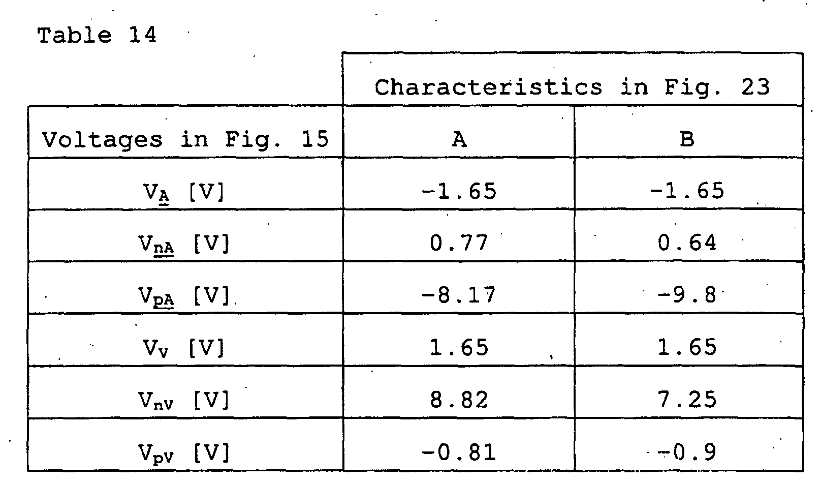
    Figs. 22 to 28 show the Vxy-IN characteristics which are measured from the chip. The voltage values in Fig. 15 for realizing the characteristics are shown in Tables 13 to 19. The characteristics correspond to the simulation characteristics of the third to seventh orders and the HSPICE simulation characteristics. Here, the current IN is obtained by the calculating formulae (4), (5), and (6), similarly to the experiment using discrete parts. The resistances in the calculating formulae (4), (5), and (6) are RG of 240 kΩ, R of 10 Ω, and output resistance Ro of 10 kΩ.
    Figure 00330001
    Figure 00340001
    Figure 00340002
    Figure 00350001
    Figure 00350002
    Figure 00360001
    Voltages in Fig. 15
    V A [V] -1.65
    V nA [V] 0.65
    V pA [V] -8.86
    VV [V] 1.65
    VnV [V] 7.79
    VpV [V] -0.81
    Another embodiment may be realized by moving in parallel the Λ-shaped and V-shaped characteristics in lateral axis direction by the following in Fig. 1.
  • (1) V xA and VyV
  • (2) V yA and VxV
  • (3) V xA , V yA , VxV, and VyV
  • According to the present invention, the control voltages in the circuit are adjusted, thereby obtaining various V-I characteristics that can be approximated to the piecewise linear functions of the third to seventh orders. Further, the various V-I characteristics are integrated as an IC form and are applied to an oscillating circuit and chaos generating circuit.
    Specifically, since the N-shaped nonlinear resistor characteristic of the N-shaped nonlinear resistor circuit according to the present invention has a negative resistance area in the center, it is widely applied to the oscillating circuit and neuron circuit. In particular, the characteristic approximates to the characteristics of the third or fifth order can form a sine wave oscillating circuit and chaos generating circuit by the combination to L or C.
    As mentioned above, the V-I characteristics approximate to the piecewise linear characteristics of the third to seventh orders are realized. Further, the V-I characteristic is easily variously changed by the external voltages. Although the fourth or sixth order characteristic is not widely used, it can easily be realized and therefore the additional application for the oscillating circuit is expected.
    Further, the N-shaped nonlinear resistor circuit using the floating gate MOSFETs of the present invention can be integrated in the standard CMOS semiconductor process and enables the integrated circuit for various applications.
    The circuit having the N-shaped voltage-current characteristic can widely be used for the sine wave oscillating circuit, double-scroll chaos circuit, and neuron circuit. This circuit structure is easily integrated as an IC form and therefore can be applied to various integrated circuits necessary for sine waves and chaos oscillating circuits. Further, the fourth or sixth order nonlinear characteristic that is not conventionally used is realized and therefore can be applied to another circuit.
    The present invention is not limited to the above embodiment, can variously be modified based on the essentials of the present invention, and various modifications are not excluded from the range of the present invention.
    As mentioned above in detail, according to the present invention, the following advantages are obtained.
  • (1) Since various N-shaped V-I characteristics are realized by the characteristics approximate to the piecewise linear functions of the third to seventh orders and they can variously be changed by the external voltages.
  • (2) The integration is realized by the standard CMOS semiconductor process and various applying circuits are integrated as a circuit.
  • Industrial Applicabilities
    A nonlinear resistor circuit using floating gate MOSFETs according to the present invention is suitable as a device indicating an N-shaped voltage-current characteristic that is important as the basic components such as an oscillating circuit, chaos generating circuit, or neuron circuit, and is expected to be applied to a voltage control sine wave oscillating circuit, voltage control chaos oscillating circuit, dynamic neuron circuit, and memory circuit.

    Claims (13)

    1. A nonlinear resistor circuit using a floating gate MOSFETs, wherein a Λ-shaped nonlinear resistor circuit using a multi-input floating gate MOSFET and a V-shaped nonlinear resistor circuit using a multi-input floating gate MOSFET are connected in parallel therewith and current of said Λ-shaped nonlinear resistor circuit and current of said V-shaped nonlinear resistor circuit are added, thus to combine various N-shaped voltage-current characteristics.
    2. The nonlinear resistor circuit using the floating gate MOSFETs according to Claim 1, wherein said N-shaped voltage current characteristic is continuously changed.
    3. The nonlinear resistor circuit using the floating gate MOSFETs according to Claim 2, wherein the voltage-current characteristics approximate to piecewise linear characteristics of third to seventh orders are realized.
    4. The nonlinear resistor circuit using the floating gate MOSFETs according to Claim 3, wherein negative resistor portions in the voltage-current characteristic of said Λ-shaped nonlinear resistor circuit and in the voltage-current characteristic of said V-shaped nonlinear resistor circuit are linear as much as possible, and both the voltage-current characteristic of said Λ-shaped nonlinear resistor circuit and the voltage-current characteristic of said V-shaped nonlinear resistor circuit are moved in parallel in the left and right directions by a voltage between an input terminal of said Λ-shaped nonlinear resistor circuit and a drain terminal of an N-channel MOSFET and a voltage between an input terminal of said V-shaped nonlinear resistor circuit and a drain terminal of a P-channel MOSFET, thus to combine the characteristic of the third order.
    5. The nonlinear resistor circuit using the floating gate MOSFETs according to Claim 3, wherein negative resistor portions in the voltage-current characteristic of said Λ-shaped nonlinear resistor circuit and the voltage-current characteristic of said V-shaped nonlinear resistor circuit are linear as much as possible, and both the voltage-current characteristic of said Λ-shaped nonlinear resistor circuit and the voltage-current characteristic of said V-shaped nonlinear resistor circuit are moved in parallel in the left and right directions by a voltage between the ground and a drain terminal of a floating gate P-channel MOSFET of said Λ-shaped nonlinear resistor circuit and a voltage between the ground and a drain terminal of a floating gate N-channel MOSFET of said V-shaped nonlinear resistor circuit, thus to combine the characteristic of the third order.
    6. The nonlinear resistor circuit using the floating gate MOSFETs according to Claim 3, wherein an inclination of a negative portion of the voltage-current characteristic of said Λ-shaped nonlinear resistor circuit or the voltage-current characteristic of said V-shaped nonlinear resistor circuit is adjusted to change the inclination of the characteristic, and the voltage-current characteristic of said Λ-shaped nonlinear resistor circuit or the voltage-current characteristic of said V-shaped nonlinear resistor circuit is moved in parallel in the left and right directions by a voltage between an input terminal of said Λ-shaped nonlinear resistor circuit and a drain terminal of an N-channel MOSFET and a voltage between an input terminal of said V-shaped nonlinear resistor circuit and a drain terminal of a P-channel MOSFET, thus to combine the fourth order characteristic.
    7. The nonlinear resistor circuit using the floating gate. MOSFETs according to Claim 3, wherein an inclination of a negative portion of the voltage-current characteristic of said Λ-shaped nonlinear resistor circuit or the voltage-current characteristic of said V-shaped nonlinear resistor circuit is adjusted to change the inclination of the characteristic, and the voltage-current characteristic of said Λ-shaped nonlinear resistor circuit or the voltage-current characteristic of said V-shaped nonlinear resistor circuit is moved in parallel in the left and right directions by a voltage between the ground and a drain terminal of a floating gate P-channel MOSFET of said Λ-shaped nonlinear resistor circuit and a voltage between the ground and a drain terminal of a floating gate N-channel MOSFET of said V-shaped nonlinear resistor circuit, thus to combine the fourth order characteristic.
    8. The nonlinear resistor circuit using the floating gate MOSFETs according to Claim 3, wherein inclinations of negative portions of both the voltage-current characteristic of said Λ-shaped nonlinear resistor circuit and the voltage-current characteristic of said V-shaped nonlinear resistor circuit are adjusted to change the inclinations of the characteristics, and both the voltage-current characteristic of said Λ-shaped nonlinear resistor circuit and the voltage-current characteristic of said V-shaped nonlinear resistor circuit are moved in parallel in the left and right directions by a voltage between an input terminal of said Λ-shaped nonlinear resistor circuit and a drain terminal of an N-channel MOSFET and a voltage between an input terminal of said V-shaped nonlinear resistor circuit and a drain terminal of a P-channel MOSFET, thus to combine the fifth order characteristic.
    9. The nonlinear resistor circuit using the floating gate MOSFETs according to Claim 3, wherein inclinations of negative portions of both the voltage-current characteristic of said Λ-shaped nonlinear resistor circuit and the voltage-current characteristic of said V-shaped nonlinear resistor circuit are adjusted to change the inclinations of the characteristics, and both the voltage-current characteristic of said Λ-shaped nonlinear resistor circuit and the voltage-current characteristic of said V-shaped nonlinear resistor circuit are moved in parallel in the left and right directions by a voltage between the ground and a drain terminal of a floating gate P-channel MOSFET of said Λ-shaped nonlinear resistor circuit and a voltage between the ground and a drain terminal of a floating gate N-channel MOSFET of said V-shaped nonlinear resistor circuit, thus to combine the fifth order characteristic.
    10. The nonlinear resistor circuit using the floating gate MOSFETs according to Claim 3, wherein an inclination of a negative portion of the voltage-current characteristic of said Λ-shaped nonlinear resistor circuit or the voltage-current characteristic of said V-shaped nonlinear resistor circuit is adjusted to change the inclination of the characteristic, and both the voltage-current characteristic of said Λ-shaped nonlinear resistor circuit and the voltage-current characteristic of said V-shaped nonlinear resistor circuit are moved in parallel in the lateral axis direction by a voltage between an input terminal of said Λ-shaped nonlinear resistor circuit and a drain terminal of an N-channel MOSFET and a voltage between an input terminal of said V-shaped nonlinear resistor circuit and a drain terminal of a P-channel MOSFET, thus to combine the sixth order characteristic.
    11. The nonlinear resistor circuit using the floating gate MOSFETs according to Claim 3, wherein an inclination of a negative portion of the voltage-current characteristic of said Λ-shaped nonlinear resistor circuit or the voltage-current characteristic of said V-shaped nonlinear resistor circuit is adjusted to change the inclination of the characteristic, and both the voltage-current characteristic of said Λ-shaped nonlinear resistor circuit and the voltage-current characteristic of said V-shaped nonlinear resistor circuit are moved in parallel in the lateral axis direction by a voltage between the ground and a drain terminal of a floating gate P-channel MOSFET of said Λ-shaped nonlinear resistor circuit and a voltage between the ground and a drain terminal of a floating gate N-channel MOSFET of said V-shaped nonlinear resistor circuit, thus to combine the sixth order characteristic.
    12. The nonlinear resistor circuit using the floating gate MOSFETs according to Claim 3, wherein inclinations of negative portions of both the voltage-current characteristic of said Λ-shaped nonlinear resistor circuit and the voltage-current characteristic of said V-shaped nonlinear resistor circuit are adjusted to change the inclinations of the characteristics, and both the voltage-current characteristic of said Λ-shaped nonlinear resistor circuit and the voltage-current characteristic of said V-shaped nonlinear resistor circuit are moved in parallel in the lateral axis direction by a voltage between an input terminal of said Λ-shaped nonlinear resistor circuit and a drain terminal of an N-channel MOSFET and a voltage between an input terminal of said V-shaped nonlinear resistor circuit and a drain terminal of a P-channel MOSFET, thus to combine the seventh order characteristic.
    13. The nonlinear resistor circuit using the floating gate MOSFETs according to Claim 3, wherein inclinations of negative portions of both the voltage-current characteristic of said Λ-shaped nonlinear resistor circuit and the voltage-current characteristic of said V-shaped nonlinear resistor circuit are adjusted to change the inclinations of the characteristics, and both the voltage-current characteristic of said Λ-shaped nonlinear resistor circuit and the voltage-current characteristic of said V-shaped nonlinear resistor circuit are moved in parallel in the lateral axis direction by a voltage between the ground and a drain terminal of a floating gate P-channel MOSFET of said Λ-shaped nonlinear resistor circuit and a voltage between the ground and a drain terminal of a floating gate N-channel MOSFET of said V-shaped nonlinear resistor circuit, thus to combine the seventh order characteristic.
    EP03701832A 2002-01-24 2003-01-22 Nonlinear resistor circuit using floating gate mosfets Expired - Lifetime EP1469600B1 (en)

    Applications Claiming Priority (3)

    Application Number Priority Date Filing Date Title
    JP2002014989 2002-01-24
    JP2002014989 2002-01-24
    PCT/JP2003/000513 WO2003063349A1 (en) 2002-01-24 2003-01-22 Nonlinear resistor circuit using floating gate mosfets

    Publications (3)

    Publication Number Publication Date
    EP1469600A1 true EP1469600A1 (en) 2004-10-20
    EP1469600A4 EP1469600A4 (en) 2005-05-18
    EP1469600B1 EP1469600B1 (en) 2007-06-27

    Family

    ID=27606102

    Family Applications (1)

    Application Number Title Priority Date Filing Date
    EP03701832A Expired - Lifetime EP1469600B1 (en) 2002-01-24 2003-01-22 Nonlinear resistor circuit using floating gate mosfets

    Country Status (5)

    Country Link
    US (1) US7023264B2 (en)
    EP (1) EP1469600B1 (en)
    JP (1) JP4662115B2 (en)
    DE (1) DE60314595T2 (en)
    WO (1) WO2003063349A1 (en)

    Cited By (1)

    * Cited by examiner, † Cited by third party
    Publication number Priority date Publication date Assignee Title
    EP1978638A3 (en) * 2007-04-06 2014-01-15 MediaTek, Inc A negative gm circuit, a filter and low noise amplifier including such a filter

    Families Citing this family (3)

    * Cited by examiner, † Cited by third party
    Publication number Priority date Publication date Assignee Title
    US7132504B2 (en) * 2003-11-12 2006-11-07 Bristol-Myers Squibb Company Hepatitis C virus inhibitors
    JP4800657B2 (en) * 2005-03-08 2011-10-26 利康 鈴木 Multi-value storage means and multi-stable circuit
    CN111626421B (en) * 2020-05-29 2022-08-05 郑州轻工业大学 A realization circuit of a fourth-order complex-valued hyperchaotic system

    Family Cites Families (5)

    * Cited by examiner, † Cited by third party
    Publication number Priority date Publication date Assignee Title
    BE556365A (en) * 1954-12-03
    JPS393222B1 (en) * 1959-06-06 1964-03-28
    US3252005A (en) * 1963-07-03 1966-05-17 Rca Corp Negative resistance circuits utilizing tunnel resistor
    DE1263080B (en) * 1966-06-09 1968-03-14 Euratom Circuit arrangement for the amplitude discrimination of pulses with the aid of a tunnel diode
    JP3007327B1 (en) * 1998-08-26 2000-02-07 科学技術振興事業団 Nonlinear resistance circuit using capacitively coupled multi-input MOSFET

    Cited By (1)

    * Cited by examiner, † Cited by third party
    Publication number Priority date Publication date Assignee Title
    EP1978638A3 (en) * 2007-04-06 2014-01-15 MediaTek, Inc A negative gm circuit, a filter and low noise amplifier including such a filter

    Also Published As

    Publication number Publication date
    WO2003063349A1 (en) 2003-07-31
    DE60314595T2 (en) 2008-03-06
    EP1469600A4 (en) 2005-05-18
    US20050121723A1 (en) 2005-06-09
    JP4662115B2 (en) 2011-03-30
    JPWO2003063349A1 (en) 2005-05-26
    US7023264B2 (en) 2006-04-04
    DE60314595D1 (en) 2007-08-09
    EP1469600B1 (en) 2007-06-27

    Similar Documents

    Publication Publication Date Title
    CN100380266C (en) Bias circuit to keep transconductance divided by load capacitance constant
    US7183867B2 (en) Voltage controlled variable capacitor
    JP3545142B2 (en) Differential amplifier
    EP0405319A1 (en) Delay circuit having stable delay time
    EP1931027A1 (en) Variable gain amplifier and its control method
    EP1858156A1 (en) Voltage controlled oscillator
    EP1435693B1 (en) Amplification circuit
    EP1469600A1 (en) Nonlinear resistor circuit using floating gate mosfets
    US6812780B2 (en) Filter circuit and detection circuit having filter circuit
    US6417655B2 (en) Common mode bias voltage generator
    US6710655B2 (en) Bipolar emitter couple pair transconductor for high speed operational amplifiers
    US7268636B2 (en) Voltage controlled oscillator
    US6879210B2 (en) Variable gain amplifier
    JPH11186860A (en) Differential amplifier circuit
    US4639617A (en) Variable-bias circuit with HF transmission path
    US20060176121A1 (en) Piezoelectric oscillator having symmetric inverter pair
    US6680651B2 (en) Current mirror and differential amplifier for providing large current ratio and high output impedence
    KR100296840B1 (en) Quartz oscillation circuit and quartz oscillation integrated circuit device
    US5438288A (en) High differential output impedance setter
    US6765418B2 (en) Clock supply bias circuit and single-phase clock drive frequency dividing circuit using the same
    CN112003611A (en) Ring oscillator and circuit implementation method
    CN213126008U (en) Ring oscillator
    US6531916B2 (en) Transconductance continuous time filter circuit
    US20250047242A1 (en) Oscillation circuit and circuit system using the same
    JP2541868B2 (en) MOS transistor circuit

    Legal Events

    Date Code Title Description
    PUAI Public reference made under article 153(3) epc to a published international application that has entered the european phase

    Free format text: ORIGINAL CODE: 0009012

    17P Request for examination filed

    Effective date: 20040720

    AK Designated contracting states

    Kind code of ref document: A1

    Designated state(s): AT BE BG CH CY CZ DE DK EE ES FI FR GB GR HU IE IT LI LU MC NL PT SE SI SK TR

    AX Request for extension of the european patent

    Extension state: AL LT LV MK RO

    A4 Supplementary search report drawn up and despatched

    Effective date: 20050405

    17Q First examination report despatched

    Effective date: 20050628

    GRAP Despatch of communication of intention to grant a patent

    Free format text: ORIGINAL CODE: EPIDOSNIGR1

    GRAS Grant fee paid

    Free format text: ORIGINAL CODE: EPIDOSNIGR3

    GRAA (expected) grant

    Free format text: ORIGINAL CODE: 0009210

    AK Designated contracting states

    Kind code of ref document: B1

    Designated state(s): CH DE FR GB LI

    REG Reference to a national code

    Ref country code: GB

    Ref legal event code: FG4D

    REG Reference to a national code

    Ref country code: CH

    Ref legal event code: EP

    REF Corresponds to:

    Ref document number: 60314595

    Country of ref document: DE

    Date of ref document: 20070809

    Kind code of ref document: P

    REG Reference to a national code

    Ref country code: CH

    Ref legal event code: NV

    Representative=s name: PATENTANWAELTE SCHAAD, BALASS, MENZL & PARTNER AG

    ET Fr: translation filed
    PLBE No opposition filed within time limit

    Free format text: ORIGINAL CODE: 0009261

    STAA Information on the status of an ep patent application or granted ep patent

    Free format text: STATUS: NO OPPOSITION FILED WITHIN TIME LIMIT

    26N No opposition filed

    Effective date: 20080328

    PGFP Annual fee paid to national office [announced via postgrant information from national office to epo]

    Ref country code: CH

    Payment date: 20120123

    Year of fee payment: 10

    Ref country code: FR

    Payment date: 20120206

    Year of fee payment: 10

    PGFP Annual fee paid to national office [announced via postgrant information from national office to epo]

    Ref country code: DE

    Payment date: 20120123

    Year of fee payment: 10

    PGFP Annual fee paid to national office [announced via postgrant information from national office to epo]

    Ref country code: GB

    Payment date: 20120120

    Year of fee payment: 10

    REG Reference to a national code

    Ref country code: CH

    Ref legal event code: PL

    GBPC Gb: european patent ceased through non-payment of renewal fee

    Effective date: 20130122

    REG Reference to a national code

    Ref country code: FR

    Ref legal event code: ST

    Effective date: 20130930

    PG25 Lapsed in a contracting state [announced via postgrant information from national office to epo]

    Ref country code: DE

    Free format text: LAPSE BECAUSE OF NON-PAYMENT OF DUE FEES

    Effective date: 20130801

    Ref country code: LI

    Free format text: LAPSE BECAUSE OF NON-PAYMENT OF DUE FEES

    Effective date: 20130131

    Ref country code: CH

    Free format text: LAPSE BECAUSE OF NON-PAYMENT OF DUE FEES

    Effective date: 20130131

    REG Reference to a national code

    Ref country code: DE

    Ref legal event code: R119

    Ref document number: 60314595

    Country of ref document: DE

    Effective date: 20130801

    PG25 Lapsed in a contracting state [announced via postgrant information from national office to epo]

    Ref country code: FR

    Free format text: LAPSE BECAUSE OF NON-PAYMENT OF DUE FEES

    Effective date: 20130131

    Ref country code: GB

    Free format text: LAPSE BECAUSE OF NON-PAYMENT OF DUE FEES

    Effective date: 20130122