EP1469509A1 - Method and device for processing substrate, and apparatus for manufacturing semiconductor device - Google Patents
Method and device for processing substrate, and apparatus for manufacturing semiconductor device Download PDFInfo
- Publication number
- EP1469509A1 EP1469509A1 EP02792066A EP02792066A EP1469509A1 EP 1469509 A1 EP1469509 A1 EP 1469509A1 EP 02792066 A EP02792066 A EP 02792066A EP 02792066 A EP02792066 A EP 02792066A EP 1469509 A1 EP1469509 A1 EP 1469509A1
- Authority
- EP
- European Patent Office
- Prior art keywords
- substrate
- processing
- gas
- oxide film
- substrate processing
- Prior art date
- Legal status (The legal status is an assumption and is not a legal conclusion. Google has not performed a legal analysis and makes no representation as to the accuracy of the status listed.)
- Withdrawn
Links
Images














Classifications
-
- H—ELECTRICITY
- H10—SEMICONDUCTOR DEVICES; ELECTRIC SOLID-STATE DEVICES NOT OTHERWISE PROVIDED FOR
- H10P—GENERIC PROCESSES OR APPARATUS FOR THE MANUFACTURE OR TREATMENT OF DEVICES COVERED BY CLASS H10
- H10P72/00—Handling or holding of wafers, substrates or devices during manufacture or treatment thereof
- H10P72/04—Apparatus for manufacture or treatment
- H10P72/0451—Apparatus for manufacturing or treating in a plurality of work-stations
- H10P72/0452—Apparatus for manufacturing or treating in a plurality of work-stations characterised by the layout of the process chambers
- H10P72/0454—Apparatus for manufacturing or treating in a plurality of work-stations characterised by the layout of the process chambers surrounding a central transfer chamber
-
- H—ELECTRICITY
- H10—SEMICONDUCTOR DEVICES; ELECTRIC SOLID-STATE DEVICES NOT OTHERWISE PROVIDED FOR
- H10P—GENERIC PROCESSES OR APPARATUS FOR THE MANUFACTURE OR TREATMENT OF DEVICES COVERED BY CLASS H10
- H10P52/00—Grinding, lapping or polishing of wafers, substrates or parts of devices
-
- H—ELECTRICITY
- H10—SEMICONDUCTOR DEVICES; ELECTRIC SOLID-STATE DEVICES NOT OTHERWISE PROVIDED FOR
- H10D—INORGANIC ELECTRIC SEMICONDUCTOR DEVICES
- H10D64/00—Electrodes of devices having potential barriers
- H10D64/01—Manufacture or treatment
- H10D64/013—Manufacture or treatment of electrodes having a conductor capacitively coupled to a semiconductor by an insulator
- H10D64/01302—Manufacture or treatment of electrodes having a conductor capacitively coupled to a semiconductor by an insulator the insulator being formed after the semiconductor body, the semiconductor being silicon
- H10D64/01332—Making the insulator
- H10D64/01336—Making the insulator on single crystalline silicon, e.g. chemical oxidation using a liquid
- H10D64/01342—Making the insulator on single crystalline silicon, e.g. chemical oxidation using a liquid by deposition, e.g. evaporation, ALD or laser deposition
-
- H—ELECTRICITY
- H10—SEMICONDUCTOR DEVICES; ELECTRIC SOLID-STATE DEVICES NOT OTHERWISE PROVIDED FOR
- H10D—INORGANIC ELECTRIC SEMICONDUCTOR DEVICES
- H10D64/00—Electrodes of devices having potential barriers
- H10D64/01—Manufacture or treatment
- H10D64/013—Manufacture or treatment of electrodes having a conductor capacitively coupled to a semiconductor by an insulator
- H10D64/01302—Manufacture or treatment of electrodes having a conductor capacitively coupled to a semiconductor by an insulator the insulator being formed after the semiconductor body, the semiconductor being silicon
- H10D64/01332—Making the insulator
- H10D64/01336—Making the insulator on single crystalline silicon, e.g. chemical oxidation using a liquid
- H10D64/01344—Making the insulator on single crystalline silicon, e.g. chemical oxidation using a liquid in a nitrogen-containing ambient, e.g. N2O oxidation
-
- H—ELECTRICITY
- H10—SEMICONDUCTOR DEVICES; ELECTRIC SOLID-STATE DEVICES NOT OTHERWISE PROVIDED FOR
- H10D—INORGANIC ELECTRIC SEMICONDUCTOR DEVICES
- H10D64/00—Electrodes of devices having potential barriers
- H10D64/60—Electrodes characterised by their materials
- H10D64/66—Electrodes having a conductor capacitively coupled to a semiconductor by an insulator, e.g. MIS electrodes
- H10D64/68—Electrodes having a conductor capacitively coupled to a semiconductor by an insulator, e.g. MIS electrodes characterised by the insulator, e.g. by the gate insulator
- H10D64/681—Electrodes having a conductor capacitively coupled to a semiconductor by an insulator, e.g. MIS electrodes characterised by the insulator, e.g. by the gate insulator having a compositional variation, e.g. multilayered
- H10D64/685—Electrodes having a conductor capacitively coupled to a semiconductor by an insulator, e.g. MIS electrodes characterised by the insulator, e.g. by the gate insulator having a compositional variation, e.g. multilayered being perpendicular to the channel plane
-
- H—ELECTRICITY
- H10—SEMICONDUCTOR DEVICES; ELECTRIC SOLID-STATE DEVICES NOT OTHERWISE PROVIDED FOR
- H10D—INORGANIC ELECTRIC SEMICONDUCTOR DEVICES
- H10D64/00—Electrodes of devices having potential barriers
- H10D64/60—Electrodes characterised by their materials
- H10D64/66—Electrodes having a conductor capacitively coupled to a semiconductor by an insulator, e.g. MIS electrodes
- H10D64/68—Electrodes having a conductor capacitively coupled to a semiconductor by an insulator, e.g. MIS electrodes characterised by the insulator, e.g. by the gate insulator
- H10D64/691—Electrodes having a conductor capacitively coupled to a semiconductor by an insulator, e.g. MIS electrodes characterised by the insulator, e.g. by the gate insulator comprising metallic compounds, e.g. metal oxides or metal silicates
-
- H—ELECTRICITY
- H10—SEMICONDUCTOR DEVICES; ELECTRIC SOLID-STATE DEVICES NOT OTHERWISE PROVIDED FOR
- H10D—INORGANIC ELECTRIC SEMICONDUCTOR DEVICES
- H10D64/00—Electrodes of devices having potential barriers
- H10D64/60—Electrodes characterised by their materials
- H10D64/66—Electrodes having a conductor capacitively coupled to a semiconductor by an insulator, e.g. MIS electrodes
- H10D64/68—Electrodes having a conductor capacitively coupled to a semiconductor by an insulator, e.g. MIS electrodes characterised by the insulator, e.g. by the gate insulator
- H10D64/693—Electrodes having a conductor capacitively coupled to a semiconductor by an insulator, e.g. MIS electrodes characterised by the insulator, e.g. by the gate insulator the insulator comprising nitrogen, e.g. nitrides, oxynitrides or nitrogen-doped materials
-
- H—ELECTRICITY
- H10—SEMICONDUCTOR DEVICES; ELECTRIC SOLID-STATE DEVICES NOT OTHERWISE PROVIDED FOR
- H10P—GENERIC PROCESSES OR APPARATUS FOR THE MANUFACTURE OR TREATMENT OF DEVICES COVERED BY CLASS H10
- H10P14/00—Formation of materials, e.g. in the shape of layers or pillars
- H10P14/60—Formation of materials, e.g. in the shape of layers or pillars of insulating materials
- H10P14/63—Formation of materials, e.g. in the shape of layers or pillars of insulating materials characterised by the formation processes
- H10P14/6302—Non-deposition formation processes
- H10P14/6304—Formation by oxidation, e.g. oxidation of the substrate
- H10P14/6306—Formation by oxidation, e.g. oxidation of the substrate of the semiconductor materials
- H10P14/6308—Formation by oxidation, e.g. oxidation of the substrate of the semiconductor materials of Group IV semiconductors
- H10P14/6309—Formation by oxidation, e.g. oxidation of the substrate of the semiconductor materials of Group IV semiconductors of silicon in uncombined form, i.e. pure silicon
-
- H—ELECTRICITY
- H10—SEMICONDUCTOR DEVICES; ELECTRIC SOLID-STATE DEVICES NOT OTHERWISE PROVIDED FOR
- H10P—GENERIC PROCESSES OR APPARATUS FOR THE MANUFACTURE OR TREATMENT OF DEVICES COVERED BY CLASS H10
- H10P14/00—Formation of materials, e.g. in the shape of layers or pillars
- H10P14/60—Formation of materials, e.g. in the shape of layers or pillars of insulating materials
- H10P14/63—Formation of materials, e.g. in the shape of layers or pillars of insulating materials characterised by the formation processes
- H10P14/6302—Non-deposition formation processes
- H10P14/6322—Formation by thermal treatments
-
- H—ELECTRICITY
- H10—SEMICONDUCTOR DEVICES; ELECTRIC SOLID-STATE DEVICES NOT OTHERWISE PROVIDED FOR
- H10P—GENERIC PROCESSES OR APPARATUS FOR THE MANUFACTURE OR TREATMENT OF DEVICES COVERED BY CLASS H10
- H10P14/00—Formation of materials, e.g. in the shape of layers or pillars
- H10P14/60—Formation of materials, e.g. in the shape of layers or pillars of insulating materials
- H10P14/63—Formation of materials, e.g. in the shape of layers or pillars of insulating materials characterised by the formation processes
- H10P14/6326—Deposition processes
- H10P14/6328—Deposition from the gas or vapour phase
- H10P14/6334—Deposition from the gas or vapour phase using decomposition or reaction of gaseous or vapour phase compounds, i.e. chemical vapour deposition
- H10P14/6339—Deposition from the gas or vapour phase using decomposition or reaction of gaseous or vapour phase compounds, i.e. chemical vapour deposition deposition by cyclic CVD, e.g. ALD, ALE or pulsed CVD
-
- H—ELECTRICITY
- H10—SEMICONDUCTOR DEVICES; ELECTRIC SOLID-STATE DEVICES NOT OTHERWISE PROVIDED FOR
- H10P—GENERIC PROCESSES OR APPARATUS FOR THE MANUFACTURE OR TREATMENT OF DEVICES COVERED BY CLASS H10
- H10P14/00—Formation of materials, e.g. in the shape of layers or pillars
- H10P14/60—Formation of materials, e.g. in the shape of layers or pillars of insulating materials
- H10P14/65—Formation of materials, e.g. in the shape of layers or pillars of insulating materials characterised by treatments performed before or after the formation of the materials
- H10P14/6502—Formation of materials, e.g. in the shape of layers or pillars of insulating materials characterised by treatments performed before or after the formation of the materials of treatments performed before formation of the materials
- H10P14/6504—In-situ cleaning
-
- H—ELECTRICITY
- H10—SEMICONDUCTOR DEVICES; ELECTRIC SOLID-STATE DEVICES NOT OTHERWISE PROVIDED FOR
- H10P—GENERIC PROCESSES OR APPARATUS FOR THE MANUFACTURE OR TREATMENT OF DEVICES COVERED BY CLASS H10
- H10P14/00—Formation of materials, e.g. in the shape of layers or pillars
- H10P14/60—Formation of materials, e.g. in the shape of layers or pillars of insulating materials
- H10P14/65—Formation of materials, e.g. in the shape of layers or pillars of insulating materials characterised by treatments performed before or after the formation of the materials
- H10P14/6516—Formation of materials, e.g. in the shape of layers or pillars of insulating materials characterised by treatments performed before or after the formation of the materials of treatments performed after formation of the materials
- H10P14/6518—Formation of materials, e.g. in the shape of layers or pillars of insulating materials characterised by treatments performed before or after the formation of the materials of treatments performed after formation of the materials by introduction of substances into an already-existing insulating layer
- H10P14/6524—Formation of materials, e.g. in the shape of layers or pillars of insulating materials characterised by treatments performed before or after the formation of the materials of treatments performed after formation of the materials by introduction of substances into an already-existing insulating layer the substance being nitrogen
- H10P14/6526—Formation of materials, e.g. in the shape of layers or pillars of insulating materials characterised by treatments performed before or after the formation of the materials of treatments performed after formation of the materials by introduction of substances into an already-existing insulating layer the substance being nitrogen introduced into an oxide material, e.g. changing SiO to SiON
-
- H—ELECTRICITY
- H10—SEMICONDUCTOR DEVICES; ELECTRIC SOLID-STATE DEVICES NOT OTHERWISE PROVIDED FOR
- H10P—GENERIC PROCESSES OR APPARATUS FOR THE MANUFACTURE OR TREATMENT OF DEVICES COVERED BY CLASS H10
- H10P14/00—Formation of materials, e.g. in the shape of layers or pillars
- H10P14/60—Formation of materials, e.g. in the shape of layers or pillars of insulating materials
- H10P14/65—Formation of materials, e.g. in the shape of layers or pillars of insulating materials characterised by treatments performed before or after the formation of the materials
- H10P14/6516—Formation of materials, e.g. in the shape of layers or pillars of insulating materials characterised by treatments performed before or after the formation of the materials of treatments performed after formation of the materials
- H10P14/6529—Formation of materials, e.g. in the shape of layers or pillars of insulating materials characterised by treatments performed before or after the formation of the materials of treatments performed after formation of the materials by exposure to a gas or vapour
- H10P14/6532—Formation of materials, e.g. in the shape of layers or pillars of insulating materials characterised by treatments performed before or after the formation of the materials of treatments performed after formation of the materials by exposure to a gas or vapour by exposure to a plasma
-
- H—ELECTRICITY
- H10—SEMICONDUCTOR DEVICES; ELECTRIC SOLID-STATE DEVICES NOT OTHERWISE PROVIDED FOR
- H10P—GENERIC PROCESSES OR APPARATUS FOR THE MANUFACTURE OR TREATMENT OF DEVICES COVERED BY CLASS H10
- H10P14/00—Formation of materials, e.g. in the shape of layers or pillars
- H10P14/60—Formation of materials, e.g. in the shape of layers or pillars of insulating materials
- H10P14/66—Formation of materials, e.g. in the shape of layers or pillars of insulating materials characterised by the type of materials
- H10P14/662—Laminate layers, e.g. stacks of alternating high-k metal oxides
-
- H—ELECTRICITY
- H10—SEMICONDUCTOR DEVICES; ELECTRIC SOLID-STATE DEVICES NOT OTHERWISE PROVIDED FOR
- H10P—GENERIC PROCESSES OR APPARATUS FOR THE MANUFACTURE OR TREATMENT OF DEVICES COVERED BY CLASS H10
- H10P14/00—Formation of materials, e.g. in the shape of layers or pillars
- H10P14/60—Formation of materials, e.g. in the shape of layers or pillars of insulating materials
- H10P14/69—Inorganic materials
- H10P14/692—Inorganic materials composed of oxides, glassy oxides or oxide-based glasses
- H10P14/6921—Inorganic materials composed of oxides, glassy oxides or oxide-based glasses containing silicon
- H10P14/6922—Inorganic materials composed of oxides, glassy oxides or oxide-based glasses containing silicon the material containing Si, O and at least one of H, N, C, F or other non-metal elements, e.g. SiOC, SiOC:H or SiONC
- H10P14/6927—Inorganic materials composed of oxides, glassy oxides or oxide-based glasses containing silicon the material containing Si, O and at least one of H, N, C, F or other non-metal elements, e.g. SiOC, SiOC:H or SiONC the material being a silicon oxynitride, e.g. SiON or SiON:H
-
- H—ELECTRICITY
- H10—SEMICONDUCTOR DEVICES; ELECTRIC SOLID-STATE DEVICES NOT OTHERWISE PROVIDED FOR
- H10P—GENERIC PROCESSES OR APPARATUS FOR THE MANUFACTURE OR TREATMENT OF DEVICES COVERED BY CLASS H10
- H10P14/00—Formation of materials, e.g. in the shape of layers or pillars
- H10P14/60—Formation of materials, e.g. in the shape of layers or pillars of insulating materials
- H10P14/69—Inorganic materials
- H10P14/692—Inorganic materials composed of oxides, glassy oxides or oxide-based glasses
- H10P14/6921—Inorganic materials composed of oxides, glassy oxides or oxide-based glasses containing silicon
- H10P14/6928—Inorganic materials composed of oxides, glassy oxides or oxide-based glasses containing silicon the material containing silicon and at least one metal element, e.g. metal silicate based insulators or metal silicon oxynitrides
- H10P14/6934—Inorganic materials composed of oxides, glassy oxides or oxide-based glasses containing silicon the material containing silicon and at least one metal element, e.g. metal silicate based insulators or metal silicon oxynitrides the material containing zirconium, e.g. ZrSiOx
-
- H—ELECTRICITY
- H10—SEMICONDUCTOR DEVICES; ELECTRIC SOLID-STATE DEVICES NOT OTHERWISE PROVIDED FOR
- H10P—GENERIC PROCESSES OR APPARATUS FOR THE MANUFACTURE OR TREATMENT OF DEVICES COVERED BY CLASS H10
- H10P50/00—Etching of wafers, substrates or parts of devices
-
- H—ELECTRICITY
- H10—SEMICONDUCTOR DEVICES; ELECTRIC SOLID-STATE DEVICES NOT OTHERWISE PROVIDED FOR
- H10P—GENERIC PROCESSES OR APPARATUS FOR THE MANUFACTURE OR TREATMENT OF DEVICES COVERED BY CLASS H10
- H10P70/00—Cleaning of wafers, substrates or parts of devices
- H10P70/10—Cleaning before device manufacture, i.e. Begin-Of-Line process
- H10P70/12—Cleaning before device manufacture, i.e. Begin-Of-Line process by dry cleaning only
-
- H—ELECTRICITY
- H10—SEMICONDUCTOR DEVICES; ELECTRIC SOLID-STATE DEVICES NOT OTHERWISE PROVIDED FOR
- H10P—GENERIC PROCESSES OR APPARATUS FOR THE MANUFACTURE OR TREATMENT OF DEVICES COVERED BY CLASS H10
- H10P72/00—Handling or holding of wafers, substrates or devices during manufacture or treatment thereof
- H10P72/04—Apparatus for manufacture or treatment
- H10P72/0402—Apparatus for fluid treatment
-
- H—ELECTRICITY
- H10—SEMICONDUCTOR DEVICES; ELECTRIC SOLID-STATE DEVICES NOT OTHERWISE PROVIDED FOR
- H10P—GENERIC PROCESSES OR APPARATUS FOR THE MANUFACTURE OR TREATMENT OF DEVICES COVERED BY CLASS H10
- H10P72/00—Handling or holding of wafers, substrates or devices during manufacture or treatment thereof
- H10P72/04—Apparatus for manufacture or treatment
- H10P72/0402—Apparatus for fluid treatment
- H10P72/0418—Apparatus for fluid treatment for etching
- H10P72/0421—Apparatus for fluid treatment for etching for drying etching
-
- H—ELECTRICITY
- H10—SEMICONDUCTOR DEVICES; ELECTRIC SOLID-STATE DEVICES NOT OTHERWISE PROVIDED FOR
- H10P—GENERIC PROCESSES OR APPARATUS FOR THE MANUFACTURE OR TREATMENT OF DEVICES COVERED BY CLASS H10
- H10P72/00—Handling or holding of wafers, substrates or devices during manufacture or treatment thereof
- H10P72/04—Apparatus for manufacture or treatment
- H10P72/0431—Apparatus for thermal treatment
- H10P72/0436—Apparatus for thermal treatment mainly by radiation
-
- H—ELECTRICITY
- H10—SEMICONDUCTOR DEVICES; ELECTRIC SOLID-STATE DEVICES NOT OTHERWISE PROVIDED FOR
- H10P—GENERIC PROCESSES OR APPARATUS FOR THE MANUFACTURE OR TREATMENT OF DEVICES COVERED BY CLASS H10
- H10P72/00—Handling or holding of wafers, substrates or devices during manufacture or treatment thereof
- H10P72/04—Apparatus for manufacture or treatment
- H10P72/0451—Apparatus for manufacturing or treating in a plurality of work-stations
- H10P72/0468—Apparatus for manufacturing or treating in a plurality of work-stations comprising a chamber adapted to a particular process
- H10P72/0474—Apparatus for manufacturing or treating in a plurality of work-stations comprising a chamber adapted to a particular process comprising at least one lithography chamber
Definitions
- the present invention generally relates to semiconductor devices and more particularly to a preprocessing method and apparatus suitable for forming an extremely thin insulation film on a semiconductor substrate.
- the thickness of the gate insulation film has to be reduced to 1 - 2nm or less when a conventional thermal oxide film is used for the gate insulation film.
- a conventional thermal oxide film is used for the gate insulation film.
- a high-dielectric material such as high-K dielectric material
- high-K dielectric material includes Ta 2 O 5 , Al 2 O 3 , ZrO 2 , HfO 2 , ZrSiO 4 , HfSiO 4 , and the like.
- the high-K dielectric film In a semiconductor device that uses such a high-K dielectric film for the gate insulation film, it is preferable to form the high-K dielectric film directly on a Si substrate for reducing the SiO 2 equivalent thickness of the insulation film.
- the metal elements in the high-K dielectric film tend to cause diffusion into the Si substrate, and there arises the problem of carrier scattering in the channel region.
- an extremely thin base oxide film having a thickness of 1nm or less, preferably 0.8 nm or less, most preferably 0.4nm or less, between the high-K dielectric gate oxide film and the Si substrate. It should be noted that this base oxide film has to be extremely thin. Otherwise, the effect of using the high-K dielectric film for the gate insulation film would be canceled out. Further, such an extremely thin base oxide film has to cover the surface of the Si substrate uniformly, without forming defects such as interface states.
- FIG.1 shows the schematic construction of a high-speed semiconductor device 1 having a high-K dielectric gate insulation film.
- the semiconductor device 1 is constructed on a silicon substrate 2 and includes a high-K dielectric gate insulation film 4 such as Ta 2 O 5 , Al 2 O 3 , ZrO 2 , HfO 2 , ZrSiO 4 , HfSiO 4 , and the like, formed on the silicon substrate 2 via a thin base oxide film 3. Further, a gate electrode 5 is formed on the high-K dielectric gate insulation film 4.
- a high-K dielectric gate insulation film 4 such as Ta 2 O 5 , Al 2 O 3 , ZrO 2 , HfO 2 , ZrSiO 4 , HfSiO 4 , and the like
- the base oxide film 3 has a larger specific dielectric constant as compared with a pure silicon oxide film. Thereby, it becomes possible to reduce the oxide-equivalent thickness of the base oxide film 3 further.
- nitrogen By introducing nitrogen into such an extremely thin base oxide film 3 with a thickness of about 1 atomic layer, it becomes possible to improve the mechanical stability at the interface to the high-K dielectric gate insulation film 4 (Lucovisky, G., et al., Appl. Phys. Lett. 74, 2005, 1999).
- the base oxide film 3 has as small thickness as possible in such a high-speed semiconductor device 1.
- this substrate manufacturing process is, while effective for reducing the defect density of the substrate, not effective for achieving the planarity, particularly the planarity of atomic-layer grade, on the substrate surface. Further, this process requires a high-temperature treatment in an electric furnace and is not suitable for constructing a cluster-type semiconductor production apparatus that conducts a single-wafer process in combination with other semiconductor manufacturing processes.
- Hi-wafer there is a known substrate manufacturing technology known as Hi-wafer in which a silicon substrate formed by a Czochralski (Cz) process is held for a long time in a hydrogen ambient at a high temperature of 1100 - 1200°C for improvement of the quality of the silicon substrate (NIKKEI MICRODEVICES, May, 1993, pp.63-64).
- NIKKEI MICRODEVICES May, 1993, pp.63-64
- Another and more specific object of the present invention is to provide a substrate processing method capable of planarizing a silicon substrate surface to the degree that atomic layer steps become observable and is suitable for constructing a cluster-type semiconductor production apparatus that conducts a single-wafer process in combination with other semiconductor processes. Further, the present invention provides a substrate processing apparatus for conducting such a substrate processing method as well as a production apparatus of semiconductor devices.
- Another object of the present invention is to provide a substrate processing method, comprising the steps of:
- Another object of the present invention is to provide a substrate processing apparatus, comprising:
- Another object of the present invention is to provide a cluster-type semiconductor production apparatus, comprising:
- Another object of the present invention is to provide a cluster-type semiconductor production apparatus, comprising:
- carbon on the substrate surface is removed preferably by a processing in an ultraviolet-excited nitrogen gas (UV-N 2 processing) in advance to the planarization processing conducted by a thermal annealing process.
- UV-N 2 processing ultraviolet-excited nitrogen gas
- formation of impurities such as SiC which causes pinning of silicon atoms at the time of the planarization processing conducted by way of suppressing flowing or sublimation of the silicon atoms, is suppressed, and the silicon atoms can move freely over the substrate surface even in the case the thermal annealing process is conducted at a relatively low temperature of about 940°C.
- the planarization process of the present invention can be conducted in an ordinary rare gas ambient such as an Ar ambient and does not require ultrahigh vacuum environment or hydrogen furnace environment, contrary to the case of conventional planarization process.
- the substrate processing method of the present invention is suitable for constructing a cluster-type semiconductor production apparatus that conducts single-wafer substrate processing in combination with other substrate processes.
- the organic substance remaining on the silicon substrate surface such as hydrocarbon or the like undergoes decomposition or depolymerization as a result of ultraviolet irradiation conducted in the nitrogen ambient.
- the organic substance is easily detached and removed from the substrate.
- the wavelength of the ultraviolet radiation used in the present invention there is caused no activation in the nitrogen gas, and thus, there occurs no formation of nitrogen film on the silicon substrate surface.
- residual carbon is removed from the substrate surface by conducting a ultraviolet nitridation (UV-N 2 ) processing on a silicon substrate surface. Thereafter, the silicon substrate surface is planarized by conducting a thermal annealing process in a rare gas.
- UV-O 2 ultraviolet radical oxidation
- FIG.2 shows the construction of a substrate processing apparatus 10 used in a first embodiment of the present invention.
- the substrate processing apparatus 10 includes a processing vessel 11 having a stage 11A holding a substrate 12 to be processed thereon, and there is provided a showerhead 11B of a material such as quartz transparent to ultraviolet radiation in the processing vessel 11.
- the showerhead 11B is provided so as to face the substrate 12 on the stage 11A.
- the processing vessel 11 is evacuated through an evacuation port 11C, and an oxidizing gas such as an oxygen gas or NO gas is supplied to the processing vessel 11 from an external gas source via the foregoing showerhead 11B.
- the processing vessel 11 is formed with an optical window 11D of a material transparent to ultraviolet radiation such as quartz above the showerhead 11B such that the optical window 11D exposes the showerhead 11B and the substrate 12 underneath the showerhead 11B. Further, the stage 11A is provided with a heater 11a for heating the substrate 12.
- an ultraviolet exposure apparatus 14 above the processing vessel 21 via an intervening connection part 13 provided in correspondence to the optical window 11D.
- the ultraviolet exposure apparatus 14 includes a quartz optical window 14A corresponding to the optical window 11D and an ultraviolet source 14B radiating ultraviolet radiation upon the substrate 12 via the optical window 11D, wherein the ultraviolet source 14B is held by a robot 14C movably in a direction parallel to the optical window 14A as is represented in FIG.2 by an arrow.
- the ultraviolet source 14B is formed of a linear optical source extending in the direction generally perpendicular to the moving direction of the ultraviolet source 14B.
- an excimer lamp having a wavelength of 172 nm.
- an inert gas such as N 2 is supplied to the connection part 13 from an external gas source (not shown) via a line 13A for avoiding the problem of absorption of the ultraviolet radiation by the oxygen in the air before the ultraviolet radiation formed by the ultraviolet radiation source 14B is introduced into the processing vessel 11 through the optical window 11D.
- the foregoing inert gas flows into the space 14D inside the ultraviolet exposure apparatus 14 through a gap formed in the mounting part of the optical window 14A of the ultraviolet exposure apparatus 14.
- a shielding plate 14F at both lateral sides of the ultraviolet source 14B, and an inert gas such as N 2 is supplied into a narrow region, which is formed between the optical window 14A opposing the ultraviolet source 14B and the shielding plate 14F with a height of about 1mm or so, via lines 14b and 14c.
- This region is also supplied with the inert gas from the line 13A, and as a result, oxygen absorbing the ultraviolet radiation is effectively purged from this region.
- the inert gas passed through the region underneath the shielding plate 14F is caused to flow into the foregoing space 14D and is then discharged to the outside of the ultraviolet exposure apparatus 14 through an evacuation port 14E formed in the ultraviolet exposure apparatus 14.
- the controller 15 controls the driving of the ultraviolet source 14B.
- FIGS.3A - 3C are AFM images showing the substrate surface for the case a silicon substrate is introduced into the UV substrate processing apparatus 10 of FIG.2 after removal of native oxide film by conducting thereto an HF (DHF) processing as the substrate 11, and a UV-N 2 processing is conducted by supplying a nitrogen gas to the showerhead 13 and driving the ultraviolet source 14B or a UV-O 2 processing is conducted by supplying an oxygen gas to the showerhead 13 and driving the ultraviolet source 14B, for the state in which a thermal annealing process is conducted further in an Ar ambient at the temperature of 1175°C under the pressure of 1060Pa for 90 seconds.
- DHF HF
- UV-N 2 processing is conducted by supplying a nitrogen gas to the showerhead 13 and driving the ultraviolet source 14B
- a UV-O 2 processing is conducted by supplying an oxygen gas to the showerhead 13 and driving the ultraviolet source 14B, for the state in which a thermal annealing process is conducted further in an Ar ambient at the temperature of 1175°C under the pressure of 10
- FIG.3A shows a comparative example in which a planarization processing is conducted on a silicon substrate after the DHF cleaning process, without processing the substrate in the substrate processing apparatus 10.
- FIG.3B shows the result of the experiment in which a silicon substrate is processed in the substrate processing apparatus 10 under the pressure of about 2.66Pa (2 x 10 -2 Torr) at the substrate temperature of 450°C while introducing an oxygen gas via the showerhead 13 with a flow rate of 150SCCM and driving the ultraviolet source 14B for 5 minutes.
- FIG.3C shows the case in which a similar processing is conducted while introducing a nitrogen gas from the showerhead 13 in place of the oxygen gas.
- a p(100) Cz wafer was used for the silicon substrate 11.
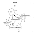
- the thermal annealing process was conducted in a substrate processing apparatus 20 of cluster type shown in FIG.4 in which the substrate processing apparatus 10 of FIG.2 is coupled to a rapid thermal processing (RTP) chamber 22 having an infrared lamp heating unit via a vacuum transportation path 21.
- RTP rapid thermal processing
- the substrate processing apparatus 20 further includes a substrate load/unload module 23 and a cooling module 24 coupled to the vacuum transportation path 21.
- both of the substrate processing apparatus 10 of FIG.2 and the rapid thermal processing chamber 22 of FIG.4 use the process temperature and pressure commonly used in ordinary semiconductor manufacturing process and there is no need of conducting a special process such as hydrogen processing.
- these processing chambers can easily constitute a cluster-type substrate processing apparatus together with other substrate processing apparatuses.
- FIGS.3A - 3C again, it can be seen that there are formed a number of island-like projecting defects on the substrate surface in the case of FIGS.3A and 3B, while in the case of FIG.3C, it will be noted that there is formed no such formation of defects at all.
- the silicon substrate is inclined slightly in the [110] direction, and as a result of this microinclination, it can be seen that' there is formed a structure in which two domains, one defining a 2 x 1 atomic terrace and the other defining a 1 x 2 atomic terrace, are arranged alternately and the foregoing two domains form a single atomic step.
- the silicon atoms rearranged on the silicon (100) surface constitute array of dimers. Because the direction of the dimers of the silicon atoms on one terrace crosses with the direction of the silicon atom dimers of an adjacent terrace perpendicularly, the edge defining the steps becomes straight or zigzag depending on whether the step edge has large energy or small energy.
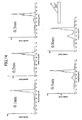
- FIGS.5A - 5C show respectively the photoelectron spectra of C 1s orbital and Si 2p orbital obtained by conducting an XPS analysis on the specimens of FIGS.3A - 3C.
- FIG.5A it can be seen that there exists a predominant photoelectron peak corresponding to the C 1s orbital caused by hydrocarbon contained in the air and adsorbed on the substrate surface during the process of transporting the substrate to the analyzer. Further, there is observed a chemical shift of the C 1s peak partially overlapped with the foregoing peak as represented by an arrow in the drawing, wherein it should be noted that this chemical shift is caused by the existence of an SiC bond. Further, it can be seen that a similar chemical shift is observed also in he spectrum of FIG.5B. In the case of FIG.5C, on the other hand, it can be seen that the spectrum is sharp, indicating that there is caused no formation of SiC bond in this specimen.
- the projecting island-like defects observed in FIGS.5A and 5B are formed of SiC. It is believed that such SiC is formed as a result of reaction of carbon atoms, originating from an organic substance such as hydrocarbon contained in the air and adsorbed on the silicon substrate surface, with the silicon atoms in the silicon substrate during the thermal annealing process.
- FIGS.3A - 3C indicate that the surface roughness of the substrate surface increases sharply in the case there exists SiC defects on the silicon substrate surface. It is believed that such SiC defects cause pinning of the silicon atoms on the silicon substrate surface and the silicon atoms are prevented from moving along the substrate surface. Further, the foregoing result indicates also that, when such SiC defects are removed, there would occur a free movement of the silicon atoms even in the temperature and pressure conditions used in ordinary semiconductor processes and that there would occur formation of atomic layer steps.
- FIGS.6A - 6D show AFM images of the substrate surface for the case carbon on the substrate surface is removed at first in the substrate processing apparatus 30 of FIG.4 by conducting the UV-N 2 processing and thereafter a thermal annealing process is conducted in the RTP apparatus 32 in an Ar ambient under the pressure of 1060Pa while changing the temperature variously.
- FIG.6A shows the case in which the thermal annealing process is conducted at 1050°C for 90 seconds
- FIG.6B shows the case in which the thermal annealing process is conducted at 1000°C for 90 seconds.
- FIG.6C shows the case in which the thermal annealing process is conducted at 950°C for 90 seconds
- FIG.6D shows the case in which the thermal annealing process is conducted at 900°C for 90 seconds.
- FIGS.6A - 6D it can be seen that there is achieved a remarkable improvement with regard to the surface roughness Rms and the maximum peak-valley amplitude PV in any of these cases as compared with the case of FIGS.3A and 3B explained previously.
- the surface roughness Rms is 0.236nm
- the peak-valley amplitude is 2.13nm
- the surface roughness Rms is 0.202nm while the maximum peak-valley amplitude is 3.43nm.
- the surface roughness Rms is 0.105nm and the peak-valley amplitude is 1.04nm.
- the surface roughness Rms is 0.141nm while the maximum peak-valley amplitude takes the value of 1.45nm.
- both the surface roughness Rms and the maximum peak-valley amplitude are minimum and a clear atomic layer step is observed.
- the experiments of FIGS.6A - 6D use the substrates of different lot with regard to the silicon substrates used in the experiments of FIGS.3A - 3C, and because of this, the direction of the microinclination is offset from the foregoing [110] direction. Because of this, the atomic layer is formed in a cross-hatch pattern rather than the terrace pattern shown in FIG.3C.
- the thermal annealing process conducted for substrate planarization after the carbon removal process conducted by the UV-N 2 processing is preferably conducted at the temperature near 950°C.
- FIGS.7A - 7C are AFM images of the substrate surface for the case a silicon substrate is subjected to a thermal annealing process for planarization after conducting various preprocessing on the silicon substrate, wherein FIG.7A shows the case in which only a native oxide removal process is applied to the substrate surface by conducting a DHF process before conducting the planarizing thermal annealing process at 950°C.
- FIG.7B shows the case in which a carbon removal process is conducted to the substrate surface in the substrate processing apparatus 10 of FIG.2 by the UV-O 2 processing while supplying an oxygen gas to the showerhead 13 after the DHF processing and thereafter a thermal annealing process is conducted at 950°C for planarization.
- FIG.7C shows the case in which the carbon removal processing is conducted on the substrate surface by the UV-N 2 processing explained before after the DHF processing and a thermal annealing process for planarization is conducted thereafter at 950°C.
- the average surface roughness Rms takes the value of 0.196nm and the maximum peak-valley amplitude PV takes the value of 3.02nm in the case of FIG.7A in which only the DHF processing is conducted, while in the case of FIG.7B in which the UV-O 2 processing is conducted, the average surface roughness Rms decreases to 0.181nm and the maximum peak-valley amplitude PV decreases to 1.69nm. Further, in the case of FIG.7C in which the UV-N 2 processing is conducted, the average surface roughness Rms is reduced further to 0.131nm and the maximum peak-valley amplitude is reduced to 1.66nm.
- FIG.8 shows the effect of carbon removal from a silicon substrate surface by various processes.
- FIG.9 shows the AFM image of FIG.7C in an enlarged scale.
- each atomic layer step has a height of 1 atomic layer (0.135nm), and the substrate is inclined slightly from the (100) surface with an angle of about 0.05°.
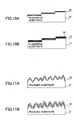
- FIGS.10A and 10B show the formation of a thin oxide film 32 on such an inclined substrate surface 31 by an UV-O 2 radial processing that uses the substrate processing apparatus 10 of FIG.2, wherein it should be noted that the inclined substrate 31 of FIGS.10A and 10B models the silicon substrate of FIG.9.
- atomic layer steps there are formed atomic layer steps repeatedly on the silicon substrate surface, and the oxide film is formed so as to cover the terrace in each of the steps.
- the silicon substrate surface is planarized to the atomic scale and atomic layer steps are appearing on the substrate surface, there appear steps also on the surface of the oxide film 32 in correspondence to the atomic layer steps.
- the atomic layer steps are transferred further to the oxide layer 33 in the form of steps.
- the substrate surface is planarized by polishing as represented in FIG.11A
- the substrate surface becomes microscopically irregular and only an irregular surface is obtained when the oxide film 32 is formed.
- the irregularity is enhanced further when the next oxide film 33 is grown on the oxide film 32 as represented in FIG.11B. Thereby, there is caused remarkable variation in the thickness of the oxide film thus formed.
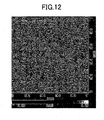
- FIG.12 shows an AFM image of an oxide film surface for the case an oxide film is grown on the structure of FIG.9 according to the model of FIGS.10A and 10B with the thickness of 0.4nm, which corresponds to two-atomic layer thickness.
- the oxide film of 0.4nm thickness was formed by using the UV radical substrate processing apparatus 10.
- the oxide film surface shows clear steps corresponding to the atomic layer steps of the underlying substrate.
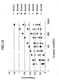
- FIG.13 shows the relationship between the film thickness and oxidation time for the case a silicon oxide film is formed on a surface of a silicon substrate processed with the UV-N 2 carbon removal processing explained before by using the substrate processing apparatus 10 of FIG.2.
- the substrate temperature was set at 450°C and an oxygen gas was supplied to the showerhead 11B while changing the ultraviolet radiation power and the oxygen gas flow rate or oxygen partial pressure variously.
- An excimer lamp having a wavelength of 172nm is used for the ultraviolet source 14B during the oxidizing processing.
- the data of Series 1 represents the relationship between the oxidation time and oxide film thickness for the case the ultraviolet radiation power is set to 5% of a reference power (50mW/cm 2 ) at the window surface of the ultraviolet radiation source 14B and the process pressure is set to 665mPa (5 mTorr) and further the oxygen gas flow rate is set to 30SCCM.
- the data of Series 2 represents the relationship between the oxidation time and oxide film thickness for the case the ultraviolet radiation power is set to zero, the process pressure is set to 133Pa (1 Torr) and the oxygen gas flow rate is set to 3SLM.
- the data of Series 3 represents the relationship between the oxidation time and oxide film thickness for the case the ultraviolet radiation power is set to zero, the process pressure is set to 2.66Pa (20 mTorr) and the oxygen gas flow rate is set to 150SCCM, while the data of Series 4 represents the relationship between the oxidation time and oxide film thickness for the case the ultraviolet radiation power is set to 100% of the reference power, the process pressure is set to 2.66Pa (20 mTorr) and further the oxygen gas flow rate is set to 150SCCM.
- the data of Series 5 represents the relationship between the oxidation time and oxide film thickness for the case the ultraviolet radiation power is set to 20% of the reference power
- the process pressure is set to 2.66Pa (20 mTorr) and the oxygen gas flow rate is set to 150SCCM
- the data of Series 6 represents the relationship between the oxidation time and oxide film thickness for the case the ultraviolet radiation power is set to 20% of the reference power
- the process pressure is set to about 67Pa (0.5 Torr) and further the oxygen gas flow rate is set to 0.5SLM.
- the data of Series 7 represents the relationship between the oxidation time and oxide film thickness for the case the ultraviolet radiation power is set to 20% of the reference power
- the process pressure is set to 665Pa (5 Torr) and the oxygen gas flow rate is set to 2SLM
- the data of Series 8 represents the relationship between the oxidation time and oxide film thickness for the case the ultraviolet radiation power is set to 5% of the reference power
- the process pressure is set to 2.66Pa (20 mTorr) and the oxygen gas flow rate is set to 150SCCM.
- the thickness of the oxide film is obtained by an XPS analysis, in view of the fact that there is no standard process of obtaining the thickness of such an extremely thin oxide film having a film thickness less than 1nm.
- a represents the detection angle of the XPS spectrum and is set to 30° in the illustrated example.
- I X+ in Eq. (1) represents an integral spectrum intensity (I 1+ +I 2+ +I 3+ +I 4+ ) of the oxide film and corresponds to the peak observed in the energy region of 102 - 104eV of FIG.15.
- I 0+ corresponds to the integral spectral peak intensity corresponding to the energy region around 100eV, wherein this spectral peak is caused by the silicon substrate.
- the oxide film thickness increases gradually from the initial thickness of 0nm with the oxidation time for the case the ultraviolet radiation power, and hence the oxygen radical density formed by the ultraviolet radiation, is set small (Series 1, 2, 3, and 8).
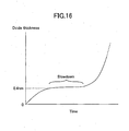
- Series 4, 5, 6 and 7 in which the ultraviolet radiation power is set to 20% or more of the reference power, on the other hand, it can be seen that there appears a slowdown of oxide film growth after the start of the growth and when the oxide film has reached a thickness of about 0.4nm as represented in FIG.16.
- the growth of the oxide film is restarted only after a certain time has elapsed in the slowdown state.
- FIG.13 or 16 means that there is a possibility of forming an extremely thin oxide film of the thickness of about 0.4nm stably in the oxidation process of a silicon substrate surface. Further, the fact that the slowdown state continues for some time as represented in FIG.16 indicates that the oxide film thus formed has a uniform thickness. Thus, according to the present invention, it is possible to form an oxide film having a thickness of about 0.4nm on a silicon substrate with uniform thickness.
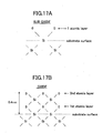
- FIGS.17A and 17B schematically depicts the manner of oxide film formation on such a silicon substrate.
- FIGS.17A and 17B schematically depicts the manner of oxide film formation on such a silicon substrate.
- the structure formed on a (100) silicon substrate is very much simplified.
- each silicon atom on the substrate surface are coordinated by two silicon atoms inside the substrate and two oxygen atoms at the substrate surface, and there is formed a sub-oxide.
- each silicon atom at the uppermost part of the silicon substrate is coordinated with four oxygen atoms and takes the stable state of Si 4+ . It is believed that this is the reason the oxidation proceeds fast in the state of FIG.17A and slows down when the state of FIG.17B has appeared.
- the thickness of the oxide film for the state of FIG.17B is about 0.4nm, while this value is in good agreement with the oxide film thickness observed for the slowdown state in FIG.13.
- the weak peak observed in the energy range of 101 - 104eV for the case the oxide film thickness is 0.1 or 0.2nm corresponds to the sub-oxide of FIG.17A.
- the peak appearing in this energy range for the case the oxide thickness has exceeded 0.3nm is thought as being caused by Si4+ and indicating the formation of an oxide film exceeding the thickness of 1 atomic layer.
- the thickness of the oxide film starts to increase again.
- FIG.18 shows the construction of a semiconductor device 30 formed by the substrate processing step according to the first embodiment of the present invention, wherein those parts of FIG.18 corresponding to the parts described previously are designated by the same reference numerals and the description thereof will be omitted.
- the semiconductor device 30 is formed on a silicon substrate 31 planarized to the degree that there appear atomic layer steps on the substrate surface and includes a base oxide film 32 formed on the silicon substrate 31 with a thickness of about 0.4nm corresponding to the thickness of 2 - 3 atomic layers, a high-K dielectric film 33 of ZrSiO x , and the like, formed on the base oxide film 32, and a gate electrode 34 of polysilicon, and the like, formed on the high-K dielectric film 33.
- FIG.19 shows the construction of a substrate processing apparatus 20A of cluster-type used for the fabrication of the semiconductor device 30 of FIG.18, wherein those parts corresponding to the parts described previously are designated by the same reference numerals and the description thereof will be omitted.
- the cluster-type substrate processing apparatus 20A includes a vacuum transportation chamber 21 to which a substrate load/unload module 23 is coupled similarly to the cluster-type substrate processing apparatus 20 explained with reference to FIG.4 and a substrate processing apparatus 10 and a substrate processing apparatus 10A similar in construction to the substrate processing apparatus 10 are coupled to the vacuum transportation chamber 21.
- the substrate processing apparatus 10 is used for conducting the UV-N 2 processing explained before while the substrate processing apparatus 10A is used to conduct the UV-O 2 processing.
- a rapid thermal processing chamber 22, a CVD chamber 25 for depositing a high-K dielectric film and a cooling chamber 24 are coupled to the vacuum transportation chamber 21.
- the substrate introduced into the substrate loading/unloading module 23 is forwarded to the UV-N 2 processing chamber 10 via the vacuum transportation path 21 for the carbon removal processing explained before.
- the substrate thus processed with the carbon removal process in the UV-N2 processing chamber 10 is then forwarded to the rapid thermal processing chamber 22 for the atomic level planarization processing.
- the substrate thus subjected to the anomic-layer level planarization is then forwarded to the UV-O 2 processing chamber 10A and a base oxide film similar to the oxide film 32 of FIG.18 and having a thickness of about 4nm is formed thereon. Further, the substrate thus formed with the base oxide film is forwarded to the CVD chamber 25 and a high-K dielectric film such as ZrO 2 , HfO 2 , ZrSiO x , HfSiO x , Ta 2 O 5 , Al 2 O 3 , and the like, is deposited one atomic layer by one atomic layer by way of atomic layer deposition (ALD) process, for example.
- ALD atomic layer deposition
- FIG.20 shows the relationship between a thermal-oxide equivalent thickness T eq and leakage current Ig for a laminated structure in which a ZrSiO x film is formed on the oxide film 32 of FIG.18 as the high-K dielectric film and an electrode film is formed further on the high-K dielectric film 34.
- the leakage current characteristics of FIG.20 are measured in the state a voltage of V fb -0.8V is applied across the electrode film and the silicon substrate, wherein V fb is a flat-band voltage used for the reference.
- FIG.20 also shows the leakage current characteristics of a thermal oxide film.
- the illustrated equivalent thickness is for the structure including both the oxide film and the ZrSiO x film.
- the leakage current density exceeds the leakage current density of the thermal oxide film in the case the oxide film is omitted and hence the film thickness of the oxide film is 0nm. Further, it can be seen that the thermal-oxide film equivalent thickness T eq also takes a large value of about 1.7nm.
- the thermal-oxide equivalent thickness T eq starts to decrease when the thickness of the oxide film is increased from 0nm to 0.4nm.
- the oxide film is interposed between the silicon substrate and the ZrSiOx film, and thus, there should be caused an increase of physical thickness.
- the observed decrease of the equivalent thickness T eq is therefore contrary to this increase of physical thickness.
- the value of the thermal-oxide equivalent thickness starts to increase again.
- the value of the leakage current is decreased with increase of the thickness, suggesting that the increase of the equivalent thickness is caused as a result of increase of the physical thickness of the oxide film.
- the oxide film thickness of about 0.4nm corresponds to the minimum of the equivalent thickness of the system formed of the oxide film and high-K dielectric film, and that the diffusion of metal element such as Zr into the silicon substrate is effectively blocked by the stable oxide film 32 shown in FIG.18. Further, it can be seen that the effect of blocking the metal element diffusion is not enhanced significantly even when.the thickness of the oxide film is increased further.
- the value of the leakage current for the case of using the oxide film of the foregoing 0.4nm thickness is smaller than the leakage current of a thermal oxide film having a corresponding thickness by the order of two.
- an insulation film having such a structure for the gate insulation film of a MOS transistor it becomes possible to minimize the gate leakage current.
- FIGS.21A - 21C show the oxide film growth occurring in each of the terrace surfaces of the silicon substrate 31 of FIG.18.
- the preferable thickness of the oxide film 32 is about two atomic layers. It should be noted that this preferable thickness includes also the case in which the oxide film 32 includes a region of 3 atomic layers in a part thereof such that the thickness of two atomic layers is maintained for the entirety of the oxide film 32. Thus, it is concluded that the preferable thickness of the oxide film 32 is in the range of 2 - 3 atomic layers.
- the silicon oxide film having the thickness of 0.4nm or 2 - 3 atomic layers can be formed stably and with excellent reproducibility.
- a silicon oxide film with a high-K dielectric film it becomes possible to realize a highly miniaturized high-speed MOS transistor having a gate insulation film wherein the effective thickness thereof is reduced.
- the oxide film 32 is not limited to such an oxide film but any other oxide film can be used as long as the oxide film is formed by an oxidation process in which the oxidation is conducted with high precision with low radical density.
- FIG.22 is a diagram explaining the condition of radical oxidation processing conducted in the UV-O 2 processing chamber 10A of FIG.19.
- the horizontal axis shows a logarithmic representation of the partial pressure of the oxygen radicals excited by the ultraviolet source in terms of Torr.
- the vertical axis represents the process time until the slowdown phenomenon shown in FIG.13 appears after the start of the processing and also the process time until such a slowdown phenomenon vanishes,.in terms of logarithmic scale.
- the oxygen partial pressure on the horizontal axis corresponds to the oxygen radical density and is determined by the driving power or ultraviolet radiation power of the ultraviolet source 324B and the ultraviolet wavelength.
- the ultraviolet source produces a photon flux of 4.34 x 10 16 /cm 2 ⁇ sec in the case a ultraviolet source producing the ultraviolet radiation power of 50mW/cm 2 at the location right underneath the window in the state of 100% driving state is used for the ultraviolet source and an oxygen gas is supplied to the substrate surface with a flow rate of 150 SCCM under the process pressure of 0.02 Torr (2.26Pa).
- a tubular lamp having a width of 2cm for the optical source 323 and irradiating a silicon wafer of 20cm diameter with such a lamp
- the average photon flux on the silicon wafer surface becomes 4.34 x 10 15 cm -2 , which is about 1/10 the photon flux value noted before.
- the amount of the radicals corresponding to the absorption of the ultraviolet radiation propagating in the processing vessel 321 for the distance'of 20cm is evaluated to be 3.65 x 10 13 cm -2 ⁇ sec by multiplying the factor of 0.0084 to the foregoing value of the photon flux of 4.34 x 10 15 cm -2 , and oxygen radicals are formed in the processing vessel with this rate.
- the flux of the oxygen gas in the processing vessel becomes 7.98 x 10 -3 cc/cm 2 ⁇ sec in terms of volume in the standard state, assuming that the showerhead has the area of 314cm 2 . In terms of the number of molecules, this value is converted to the value of 2.138 x 10 17 cm -2 ⁇ sec.
- the radical density is calculated also for other various conditions.
- the slowdown effect appears immediately after the start of the process similarly to the case of FIG.13 in the event the radical density in the processing vessel is large.
- the slowdown phenomenon appears after a long time has elapsed after start of the process. This corresponds to the situation that the growth rate of the oxide film is large in the case of large radical density and the stationary thickness of 0.4nm is reached in short time, while in the case the radical density is small, it takes a long time until the foregoing stationary thickness of 0.4nm is achieved because of the small oxide film growth rate.
- the slowdown duration defined as the duration after the appearance of the slowdown phenomenon up to the vanishing of the slowdown phenomenon changes also with the radical density such that the slowdown duration is decreased when the radical density is large and is increased when the radical density is small.
- FIG.22 which shows the example of conducting the oxidation of the substrate at 450°C by the radical oxidation process while using the ultraviolet radiation of the 172nm wavelength
- the lower limit of the radical partial pressure is determined to be 1 x 10 -4 mTorr (133 x 10 -7 Pa) assuming that the tolerable process time is 5 minutes (300 seconds) or less.
- the upper limit of the radical partial pressure is determined to be 1 mTorr (1.33 x 10 -3 Pa) assuming that the necessary slowdown interval is 100 seconds or more.
- the ultraviolet radiation power corresponding to this is determined to be 5 - 50mW ⁇ cm -2 in the region right underneath the optical source 14B.
- the interval between the two lines respectively defining the appearance and vanishing of the slowdown phenomenon is decreased with the radical partial pressure. This, however, is merely an apparent effect caused by the fact that the vertical axis and the horizontal axis of FIG.22 are represented with logarithmic scale.
- the duration of the stationary interval is in fact decreased with the radical partial pressure.
- the oxygen partial pressure in the case of using an ultraviolet radiation source of 146nm wavelength for the ultraviolet source, it is necessary to set the oxygen partial pressure to the range of 0.05 - 50 mTorr (6.7mPa - 6.7Pa) in view of the large optical absorption larger by 25 times as compared with the case of the wavelength of 172nm.
- the nitrogen atoms should not enter the silicon substrate. Further, the planarity of the interface between the silicon substrate 2 and the base oxide film 3 should not be degraded.
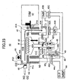
- FIG.23 shows the general construction of a substrate processing apparatus 40 according to the third embodiment of the present invention for forming the extremely thin base oxide film 12 on the silicon substrate 11 together with the oxynitride film 12A.
- the substrate processing apparatus 40 includes a processing vessel 41 accommodating therein a stage 42 equipped with a heater 42A such that the stage 42 is movable vertically between a process position and a substrate load/unload position.
- the stage 42 is rotated by a drive mechanism 42C, and the processing vessel 41 defines a process space 41B therein together with the stage 42.
- a magnetic seal 48 at the connecting part of the stage 42 and the drive mechanism 42C such that the magnetic seal 48 separates a magnetic seal chamber 42B held in a vacuum environment from the drive mechanism 42C formed in the atomic environment. Because the magnetic seal 48 is a liquid, the stage 42 is held so as to be able to rotate freely.
- the stage 42 is held at the process position and there is formed a load/unload chamber 41C underneath the stage 42 for loading and unloading.the substrate.
- the processing vessel 41 is connected to a substrate transfer unit 47 via a gate valve 47A, and thus, the substrate W is transported to the stage 42 from the substrate transfer unit 47 via the gate valve 47A in the state that stage 42 has been lowered to the load/unload chamber 41C. Further, the processed substrate W is transferred to the substrate transfer unit 47 from the stage 42.
- a turbo molecular pump 43B is connected to the evacuation port 41A via the valve 43A.
- the turbo molecular pump 43B is further connected to a pump 44 formed of a dry pump and a mechanical booster pump via a valve 43C, and the pressure inside the process space 41B can be reduced to the level of 1.33 x 10 -1 - 1.33 x 10 -4 Pa (10 -3 - 10 -6 Torr) by driving the turbo molecular pump 43B and the dry pump 44.
- evacuation port 41A is connected also to the pump 44 directly via a valve 44A and an APC 44B, and thus, the pressure of the process space is reduced to the level of 1.33Pa - 1.33kPa (0.01 - 100 Torr) by the pump 44 when the valve 44A is opened.
- the processing vessel 41 is provided with a process gas supplying nozzle 41D at the side opposite to the evacuation port 41A across the substrate W, and an oxygen gas is supplied to the process gas supplying nozzle 41D.
- the oxygen gas thus supplied to the process gas supplying nozzle 41D is caused to flow in the process space 41B along the surface of the substrate W and is evacuated from the evacuation port 41A.
- the substrate processing apparatus 40 of FIG.23 is provided with an ultraviolet optical source 45 having a quartz window 45A on the processing vessel 21 in correspondence to the region located between the process gas supplying nozzle 41D and the substrate W.
- the oxygen gas introduced in to the process space 41B from the process gas supplying nozzle 41D is activated, there are formed oxygen radicals and the oxygen radicals thus formed are caused to flow along the surface of the substrate W.
- a radical oxide film on the surface of the substrate W with a thickness of 1nm or less, particularly with the thickness of about 0.4nm, which corresponds to the thickness of 2 - 3 atomic layers.
- the processing vessel 41 is provided with a remote plasma source 46 at the side thereof opposite to the evacuation port 41A with respect to the substrate W.
- a remote plasma source 46 at the side thereof opposite to the evacuation port 41A with respect to the substrate W.
- nitrogen radicals are formed by supplying a nitrogen gas to the remote plasma source 46 together with an inert gas such as Ar and by activating the nitrogen gas thus supplied with plasma.
- the nitrogen radicals thus formed are caused to flow along the surface of the substrate W and causes nitridation of the substrate surface.
- oxygen By introducing oxygen into the remote plasma source 46 in place of nitrogen, it is also possible to oxidize the substrate surface.
- a purge gas line 41c for purging the load/unload chamber 41C with a nitrogen gas.
- a purge line 42b for purging the magnetic seal chamber 42B with a nitrogen gas and an evaluation line 42c of the purge gas.
- the evacuation line 42c is connected to a turbo molecular pump 49B via a valve 49A, and the turbo molecular pump 49B is connected to the pump 44 via a valve 49C. Further, the evacuation line 42c is connected directly to the pump 44 via a valve 49D. With this, it becomes possible to maintain the magnetic seal chamber 42B at various pressures.
- the load/unload chamber 41C is evacuated by the pump 44 via the valve 44C or by the turbo molecular pump 43B via the valve 43D. Further, in order to avoid contamination in the process space 41B, the load/unload chamber 41C is held at a lower pressure than the process space 41B, and the magnetic seal chamber 41B is held at a further lower pressure than the load/unload chamber 41C by a conducting differential evacuation process.
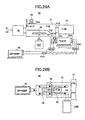
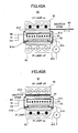
- FIGS.24A and 24B are diagrams showing the radical oxidation process of the substrate W by using the substrate processing apparatus 40 of FIG.23 respectively in a side view and a plan view.
- a silicon substrate applied with the carbon removal processing and planarization processing explained with reference to the previous embodiment is introduced into the processing vessel 41 as a substrate W to be processed; and an oxygen gas is supplied to the process space 41B from the process gas supplying nozzle 41D.
- Oxygen thus supplied is evacuated, after flowing along the surface of the substrate W, via the evacuation port 41A, turbo molecular pump 43B and the pump 44.
- the process pressure in the process space 41B is set to the level of 1 x 10 -3 - 10 -6 Torr, which is needed for the oxidation of the substrate by oxygen radicals.
- the ultraviolet source 45 preferably the one that produces ultraviolet radiation of 172nm wavelength, is activated, and oxygen radicals are formed in the oxygen gas flow thus formed.
- the oxygen radicals thus formed cause oxidation of the substrate surface as they are caused to flow along the rotating substrate W.
- UV-O 2 processing a very thin oxide film having a thickness of 1nm or less, particularly the thickness of about 0.4nm corresponding to the thickness of 2 - 3 atomic layers, is formed on a surface of a silicon substrate stably and with excellent reproducibility.
- FIG.24B shows the construction of FIG.24A in a plan view.
- the ultraviolet source 45 is a tubular light source extending in the direction crossing the direction of the oxygen gas flow. Further, it can be seen that the turbo molecular pump 23B evacuates the process space 41B via the evacuation port 41A. Further, it should be noted that the evacuation path, designated in FIG.24B by a dotted line and extending directly from the evacuation port 41A to the pump 44, is closed by closing the valve 44A.
- the turbo molecular pump 23B is provided in an arrangement so as to extend laterally from the processing vessel. Thereby, the turbo molecular pump 43B successfully avoids the substrate transfer unit 47.
- a very thin silicon oxide film is formed on the surface of the silicon substrate W in correspondence to each of the terraces shown in FIG.18.
- the slowdown phenomenon explained previously with reference to FIGS.13 or FIG.16, and thus, it becomes possible to set the thickness of the oxide film to the thickness of about 0.4nm corresponding to 2 - 3 atomic layers by utilizing such a slowdown phenomenon as explained before.
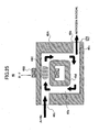
- FIG.25 shows the construction of a remote plasma source 46 used in the substrate processing apparatus 40 of FIG.23.
- the remote plasma source 46 includes a block 46A typically formed of aluminum in which a gas circulating passage 46a is formed together with a gas inlet 46b and a gas outlet 46c communicating therewith. Further, there is formed a ferrite core 46B on a part of the block 46A.
- a fluorocarbon resin coating 46d on the inner surfaces of the gas circulating passage 46a, gas inlet 46b and the gas outlet 46c, and plasma 46C is formed in the gas circulating passage 46a by supplying a high-frequency power of 400kHz frequency to the coil wound around the ferrite core 46B.
- nitrogen radicals and also nitrogen ions are formed in the gas circulating passage 46a, wherein the nitrogen ions are annihilated as they are circulated along the circulating passage 46a and the gas outlet 46c ejects nitrogen radicals N 2 * primarily.
- charged particles such as nitrogen ions are eliminated in the construction of FIG.25 by providing an ion filter 46e at the gas outlet 46c in the state that the ion filter 46e is connected to the ground. Thereby, only the nitrogen radicals are supplied to the process space 41B.
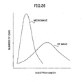
- FIG.26 shows the relationship between the number of ions and the electron energy formed by the remote plasma source 46 of FIG.25 in comparison with the case of using a microwave plasma source.
- ionization of nitrogen molecules is facilitated in the case.the plasma is excited by a microwave power, and as a result, there are formed a very large amount of nitrogen ions.
- the plasma is excited by a high-frequency power of 500kHz or less in the frequency, on the other hand, the number of the nitrogen ions formed by the plasma is reduced significantly.
- a high vacuum environment of 1.33 x 10 -3 - 1.33 x 10 -6 Pa (10-1 - 10 -4 Torr) is needed, while in the case of a high-frequency plasma process, the process can be conducted at a relatively high pressure of 13.3 - 13.3kPa (0.1 - 100 Torr).
- Table 2 compares the ionization energy conversion efficiency, pressure range capable of causing electric discharge, plasma power consumption and process gas flow rate between the case of exciting plasma by a microwave and the case of exciting plasma by a high-frequency power.
- ionization energy conversion efficiency pressure range causing electric discharge plasma power consumption process gas flow rate microwave 1.00x10 -2 0.1m - 0.1Torr 1 - 500W 0 - 100SCCM RF-wave 1.00x10 -7 0.1 - 100Torr 1 - 10kW 0.1 - 10SLM
- the ionization energy conversion efficiency is reduced to about 1 x 10 -7 in the case of the RF-excited plasma as compared with respect to the value of about 1 x 10 -2 for the case of the microwave-excited plasma.
- the pressure range causing the electric discharge is about 0.1 - 100 Torr (13.3Pa - 13.3kPa) for the case of the RF-excited plasma, while in the case of the microwave-excited plasma, the pressure range is about 0.1 mTorr - 0.1 Torr (133mPa - 13.3Pa).
- the plasma power consumption is increased in the case of the RF-excited plasma as compared with the case of the microwave-excited plasma and that the process gas flow rate'for the case of the RF-plasma processing becomes much larger than the process gas flow rate for the case of the microwave plasma.
- the nitridation processing of the oxide film is conducted not by nitrogen ions but by the nitrogen radicals N 2 *.
- the number of the excited nitrogen ions is suppresses as small as possible. This is also preferable in the viewpoint of minimizing damages caused in the substrate.
- the number of the excited nitrogen radicals is small and is highly suitable for nitriding the extremely thin base oxide film formed underneath the high-K dielectric gate insulation film with the thickness of only 2 - 3 atomic layers.
- FIGS.28A and 28B show the radical nitridation processing conducted by the substrate processing apparatus 40 of FIG.23 respectively in a side view and a plan view.
- the remote plasma radical source 46 is supplied with an Ar gas and a nitrogen gas and nitrogen radicals are formed as a result of excitation of plasma with the high frequency power of several hundred kilohertz frequency.
- the nitrogen radicals thus formed are caused to flow along the surface of the substrate W and are evacuated via the evacuation port 41A and the pump 44.
- the process space 41B is held at a process pressure in the range of 1.33Pa - 1.33kPa (0.01 - 10 Torr) suitable for the radical nitridation of the substrate W.
- the nitrogen radicals thus formed cause nitridation in the surface of the substrate W as they are caused to flow along the surface of the substrate W.
- FIG.29A shows the nitrogen concentration profile in an oxide film for the case the oxide film formed on a silicon substrate by a thermal oxidation process with a thickness of 2.5nm is subjected to an RF-N 2 processing in the substrate processing apparatus 40 of FIG.23 by using the RF remote plasma source 46 of FIG.25 under the condition represented in Table 3.
- FIG.29B shows the relationship between the nitrogen concentration profile and the oxygen concentration profile in the same oxide film.
- the RF-N 2 processing is conducted in the substrate processing apparatus 40 under the pressure of 1 Torr (133Pa) while supplying nitrogen with a flow rate of 50SCCM and Ar with a flow rate of 2SLM, wherein it should be noted that the internal pressure of the process space 41B is reduced once to the level of about 10 -6 Torr (1.33 x 10 -4 Pa) before the commencement of the nitridation process such that oxygen or water remaining in the process space 41B is purged sufficiently. Because of this, any residual oxygen in the process space 41B is diluted with Ar or nitrogen in the nitridation process (RF-N 2 process), which is conducted at the pressure of about 1 Torr. Thereby, the concentration of residual oxygen, and hence the thermodynamic activity of the residual oxygen, is very small at the time of the foregoing nitridation processing.
- the process pressure at the time of the nitridation process is generally the same as the purging pressure, and thus, residual oxygen maintains a large thermodynamic activity in the plasma ambient.
- the concentration of nitrogen incorporated into the oxide film is limited in the case the nitridation processing is conducted by the microwave plasma and that no substantial nitridation takes place in the oxide film.
- the nitrogen concentration level changes linearly with depth in the oxide film and that a concentration level of near 20% is achieved at the surface part of the oxide film.
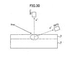
- FIG.30 shows the principle of the measurement of FIG.29A conducted by the XPS (X-ray photo spectrometry) analysis.
- an X-ray is radiated to the specimen in which the oxide film 3 is formed on the silicon substrate 2 with a predetermined angle, and detectors DET1 and DET2 are used to detect the spectrum of the excited X-rays with various angles.
- the detector DET1 set to a deep detection angle of 90 degrees detects the excited X-ray that has traveled through the oxide film 12 with minimum path length.
- the X-ray spectrum detected by the detector DET1 contains information about the deep part of the oxide film 3 with relatively large proportion.
- detector DET2 set to a shallow detection angle detects the X-ray traveled over a long distance in the oxide film 3.
- the detector DET2 mainly detects the information about surface part of the oxide film 3.
- FIG.29B shows the relationship between the nitrogen concentration and oxygen concentration in the oxide film.
- the oxygen concentration is represented by the X-ray intensity corresponding to the O 1s orbital.
- FIG.29B it can be seen that there occurs decrease of oxygen concentration with increase of nitrogen concentration in the case the nitridation processing is conducted by the RF-N 2 processing that uses the RF-remote plasma, indicating that there occurs substitution of oxygen atoms with the nitrogen atoms in the oxide film.
- the nitridation is conducted by the microwave plasma processing, on the other hand, no such substituting relationship is observed and no relationship of oxygen concentration decreasing with increasing nitrogen concentration is observed.
- FIG.29B it is also noted that there is an increase of oxygen concentration for the case in which nitrogen is incorporated with 5 - 6% by the microwave nitridation processing. This indicates that there occurs increase of thickness of the oxide film with nitridation.
- Such an increase of the oxygen concentration associated with the microwave nitridation processing is believed to be caused as a result of the high activity of oxygen or water remaining in the process space, which in turn is caused as a result of use of high vacuum environment for the nitridation processing and absence of dilution of residual oxygen or water with Ar gas or nitrogen gas, unlike the case of the high-frequency remote radical nitridation processing.
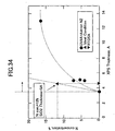
- FIG.31 shows the relationship between the nitridation time and the nitrogen concentration in the film for the case an oxide film is formed by the substrate processing apparatus 40 of FIG.33 to the thickness of 4 ⁇ (0.4nm) and 7 ⁇ (0.7nm) and nitridation is conducted further to the oxide film by the RF-N 2 processing of FIGS.28A and 28B while using the remote plasma source 26.
- FIG.32 shows the segregation of nitrogen to the surface of the oxide film caused as a result of the nitridation processing of FIG.31. It should be noted that FIGS.31 and 32 also show the case in which the oxide film is formed by a rapid thermal oxidation processing to the thickness of 5 ⁇ (0.5nm) and 7 ⁇ (0.7nm).
- the nitrogen concentration in the film increases with the nitridation time in any of the oxide films, while it is also noted that, because of the small oxide thickness such as 0.4nm corresponding to the two atomic layer thickness for the case of the oxide film formed by the UV-O 2 oxidation processing, or for the case of the thermal oxide film having a thickness of 0.5nm near the foregoing thickness of 0.4nm, a higher nitrogen concentration is achieved as compared with oxide films formed at the same condition.
- FIG.32 shows the result of detection of nitrogen concentration for the case the detectors DET1 and DET2 of FIG.30 are set to 30 degrees and 90 degrees respectively.
- the vertical axis represents the X-ray spectral intensity from the nitrogen atoms segregated to the film surface obtained with the detection angle of 30 degrees divided by the X-ray spectral intensity of the nitrogen atoms distributed throughout the entire film. In the case this value is 1 or more, there is caused segregation of nitrogen to the film surface.
- FIG.33 shows the wafer-to-wafer variation of the film thickness of the oxynitride film thus obtained, wherein the result of FIG.33 is obtained for the case in which the UV-O 2 processing is conducted in the construction of FIG.23 by driving the ultraviolet source 45 such that an oxide film is formed to have the thickness of 0.4nm as measured by the XPS analysis and in which the RF-N 2 processing is conducted to the oxide film thus formed by driving the remote plasma source 46 such that the oxide film is converted to an oxynitride film containing nitrogen atoms with about 4%.
- the vertical axis represents the film thickness obtained for the oxynitride film thus obtained by ellipsometry, wherein it can be seen that the film thickness is uniform and has a value of about 8 ⁇ (0.8nm).
- FIG.34 shows the result of examination with regard to the increase of film thickness for the case an oxide film is formed on a silicon substrate in the substrate processing apparatus 40 of FIG.23 with the thickness of 0.4nm by the UV-O 2 processing while using the ultraviolet source 45 and further an RF-N 2 processing is applied to the oxide film thus formed while using the remote plasma source 46.
- the oxide film has increased the thickness thereof from the initial thickness (the thickness in the state before the RF-N 2 processing) of 0.38nm to about 0.5nm in the state nitrogen atoms are introduced by the RF-N 2 processing with the concentration of 4 - 7%.
- the nitrogen atoms are introduced to the level of about 15% by the RF-N 2 processing, on the other hand, it can be seen that the film thickness increases to about 1.3nm. In this case, it is believed that the nitrogen atoms thus introduced into the oxide film form a nitride film by causing penetration into the silicon substrate after passing through the oxide film.
- the relationship between the nitrogen concentration and film thickness is represented also for an ideal model structure in which only one layer of nitrogen atoms are introduced into the oxide film of 0.4nm thickness by ⁇ .
- the film thickness after introduction of the nitrogen atoms becomes about 0.5nm in this ideal model structure.
- the increase of the film thickness for this model case becomes about 0.1nm, and the nitrogen concentration becomes about 12%.
- the increase of film thickness is preferably suppressed to the value of 0.1 - 0.2nm close to the foregoing value in the case the substrate processing apparatus 40 of FIG.23 is used for the nitridation of the oxide film. In this state, it is evaluated that the maximum amount of the nitrogen atoms incorporated in to the film would be about 12% in the maximum.
- FIGS.35A and 35B show the result of measurement of nitrogen concentration distribution and film thickness distribution of an oxynitride film for the case the oxynitride film is formed from an oxide film formed on the silicon substrate W in the substrate processing apparatus 40 of FIG.23 to the thickness of 2nm while rotating the silicon substrate W by the drive mechanism 42C.
- the experiment of FIGS.35A and 35B is conducted at the substrate temperature of 450°C under the pressure of 133Pa while rotating the silicon substrate formed with the oxide film with the thickness of 2nm, while supplying an Ar gas and a nitrogen gas with the respective flow rates of 2SLM and 50SCCM.
- the bright part represents the part where there is caused nitrogen concentration.
- FIG.35B shows the thickness of the oxynitride film obtained by the ellipsometry and the nitrogen concentration obtained by the XPS analysis.
- FIGS.35A and 35B shows that it is possible to realize a generally uniform nitrogen distribution over the entire surface of the substrate W even in the case of using the substrate processing apparatus 40, in which an asymmetric radical flow is caused, by rotating the substrate W and optimizing the flow rate of the Ar gas and the flow rate of the nitrogen gas.
- a CVD process is used to form such a high-K dielectric film 4.
- a ZrO 2 film for example, ZrCl 4 or other gaseous source containing Zr is used and the ZrO 2 film is deposited by oxidizing such a gaseous source.
- the formation of such a high-K dielectric film 13 is conducted subsequent to the nitridation process of the radical oxide film shown in FIGS.28A and 28B, without contacting the substrate to the external air.
- the substrate processing apparatus 40 of FIG.23 is integrated into a cluster-type substrate' processing system that includes a CVD chamber. Further, it is preferable that such a cluster-type substrate processing includes therein the organic removal process by the UV-N 2 processing explained before and the atomic-layer level planarization processing.
- FIG.36 shows the schematic construction of such a cluster-type substrate processing system 50 according to a fourth embodiment of the present invention.
- the cluster-type substrate processing system 50 includes cassette module 51 for loading and unloading a substrate W and a substrate transfer chamber 52 connected to the cassette module 51 via respective gate valve, wherein the substrate transfer chamber 52 is further connected to: a substrate cleaning chamber 53; a UV-N 2 processing chamber 54 for conducting the organic removal processing explained with reference to the previous embodiment; a rapid thermal processing (RTP) chamber 55 for conducting the planarization process; a UV-O 2 /PLASMA-N 2 processing chamber 56 including therein the substrate processing apparatus 40 of FIG.23 and conducting the formation of the base oxide film by the UV-O 2 radical processing and the nitridation of the base oxide film by the plasma radicals; a CVD chamber 57 for depositing a high-K dielectric film by an ALD process and the like; and a cooling chamber 58.
- a substrate cleaning chamber 53 for loading and unloading a substrate W and a substrate transfer chamber 52 connected to the cassette module 51 via respective gate valve, wherein the substrate transfer chamber 52 is further connected to: a substrate cleaning chamber 53
- the substrate W introduced into the substrate transfer chamber 52 from the cassette module 51 is first forwarded to the substrate cleaning chamber 53 for removing a native oxide film or organic contamination therefrom.
- the substrate W is transported to the UV-N 2 processing chamber 54 for removal of the organic substance.
- the substrate W is transported to the RTP chamber 55 via the substrate transportation chamber 55 for atomic-layer level planarization.
- the substrate W thus planarized is then transported to the UV-O 2 /PLASMA-N 2 processing chamber 34 via the substrate transfer chamber 52 and the base oxide film 3 and the nitride film 3A of FIG.1 are formed.
- the substrate W is forwarded to the CVD chamber 57 through the substrate transfer chamber 52 for formation of the high-K dielectric film 4.
- the substrate W is further forwarded t the thermal processing chamber 55 for crystallization and oxygen-defect compensation processing.
- the substrate W is transported to the cassette module 51 through the substrate transfer chamber 52.
- each of the processing chambers 53 - 56 is provided, in the cluster-type substrate processing apparatus 50 of FIG.36, with various cooperating devices, and because of this, each processing chambers requires an area represented in FIG.36 by a broken line, in addition to the area of the chamber itself. Thereby, it should be noted that available space is substantially limited at the side of the processing chamber close to the substrate transfer chamber 52 because of the reduced separation to adjacent chambers.
- the processing chamber 42 is connected to the substrate transfer chamber 52, wherein there arises a problem in that the turbo molecular pump 43B, extending laterally to the processing chamber 41 at the side thereof close to the substrate transfer chamber 52 as represented in FIG.24B, may cause an interference with the adjacent processing chamber.
- turbo molecular pump 43B In order to conduct fast depressurization of the processing vessel 41, it is necessary that the turbo molecular pump 43B is provided close to the evacuation port 41A, while there exists no space available for this purpose because of the fact that various devices including the transportation robot are provided underneath the substrate transfer chamber 52. Further, there is no available space underneath the processing vessel 41 for the turbo molecular pump 43B because of the fact that various devices including the substrate rotating mechanism 42C are provided underneath the processing vessel 41.
- FIG.37A and 37B are diagrams showing the construction of a substrate processing apparatus 40A according to an embodiment of the present invention respectively in a side view and a plan view, wherein those parts of FIGS.37A and 37B explained before are designated by the same reference numerals and the description thereof will be omitted.
- the substrate processing apparatus 40 disposes the turbo molecular pump 43B at the outer side of the substrate processing vessel 41, in other word the side opposite to the substrate transfer unit 47 where there is an available space when the substrate processing apparatus 40 is used to construct the cluster type substrate processing system such as the one shown in FIG.36.
- the evacuation port 41E in the processing vessel 21 at the outer side thereof, in other words at the side opposite to the substrate transfer chamber.
- the process gas nozzle 41D and the ultraviolet optical source 45 are provided to the side close to the substrate transfer chamber 47 with respect to the substrate W such that the oxygen radicals are caused to flow along the surface of the substrate W to the evacuation port 41E.
- turbo molecular pump 43B is connected to the bottom part of the processing vessel 41 via the valve 43A in a vertical state, in other words the state in which the inlet and the outlet are aligned vertically. Further, it should be noted that the outlet port of the turbo molecular pump 43B is connected to the evacuation line extending from the evacuation port 41A of the processing vessel 41 to the pump 44 via the valve 44A at the part behind the valve 44A.
- FIGS.38A and 38B are diagrams showing the process of forming the base oxide film 3 of FIG.1 conducted by using the substrate processing apparatus 40.
- valves 43A and 43B are opened and the valve 44A is closed in the base oxide film formation process.
- the process space 43B is evacuated to the high-degree vacuum state of 1.33 x 10 -1 - 1.33 x 10 -4 Pa (10 -3 - 10 -6 Torr) by the turbo molecular pump 43B at the foregoing evacuation port 41E, and the oxygen gas is introduced into the process space 41B from the process gas nozzle 41D in this state.
- driving the ultraviolet source 45 with a suitable energy while rotating the substrate W by the substrate rotating mechanism 42C, there is caused a flow of oxygen radicals to the evacuation port 42E along the substrate surface, and the substrate surface is oxidized uniformly.
- FIGS.39A and 39B show the process of forming the oxynitride film 12A by using the substrate processing apparatus 40 of the present embodiment after the step of FIGS.38A and 3.8B by nitriding the surface of the base oxide film 12 thus formed.
- valve 43A and 43C are closed and the valve 44A is opened in the nitridation process.
- the turbo molecular pump 43B is disconnected from the evacuation system and the process space 41B is evacuated directly by the pump 44 to the pressure of 1.33Pa - 13.3kPa (0.01 - 100Torr).
- an Ar gas and a nitrogen gas are supplied to the remove plasma source 46, and nitrogen radicals are formed by applying a high-frequency excitation to the nitrogen gas.
- the nitrogen radicals thus formed are caused to flow along the surface of the substrate W to the evacuation port 41A, and there is caused a uniform nitridation on the surface of the rotating substrate W.
- the surface of the base oxide film 3 of FIG.1 is converted to the oxynitride film 3A.
- the substrate processing apparatus 40A of the present embodiment for the processing chamber 56 in the cluster type substrate processing system 50 of FIG.36, it becomes possible to form the high-K dielectric film 4 such as ZrO 2 , HfO 2 , Ta 2 O 5 , ZrSiO 4 , HfSiO 4 , Al 2 O 3 , and the like, on the base oxide film 3 that includes therein the oxynitride film 3A.
- the high-K dielectric film 4 such as ZrO 2 , HfO 2 , Ta 2 O 5 , ZrSiO 4 , HfSiO 4 , Al 2 O 3 , and the like
- the substrate processing apparatus 40A was explained with regard to the formation of very thin base oxide film.
- the present invention is not limited to such a specific embodiment and the present invention can be applied to the process of forming a high-quality oxide film, nitride film or oxynitride film on a silicon substrate or a silicon layer with a desired thickness.
- FIGS.40A and 40B show the construction of a UV-N 2 substrate processing apparatus 60 according to a fifth embodiment of the present invention.
- the substrate processing apparatus 60 is a modification of the substrate processing apparatus 10 of FIG.2 and includes a processing vessel 61 holding a substrate 62 to be processed and evacuated at an evacuation port 61A, wherein the substrate 62 is held on an optically transparent stage 61B of a quartz glass in the processing vessel 61. Further, there is provided a quartz glass showerhead 61C in the processing vessel 61 so as to face the substrate 62.
- a quartz glass window 61D so as to face the substrate 62 and an ultraviolet source 62, formed of an array of tubular excimer lamps, is provided outside the quartz glass window 61D. Further, there is formed another quartz glass window 61E at the bottom of the processing vessel 61 in correspondence to the bottom surface of the substrate 62, and an infrared heating lamp 63 is provided outside the quartz glass window 61E. Between the quartz glass window 61D and the ultraviolet source 62, there is provided a movable shutter mechanism 64 for protection of the ultraviolet source 62.
- a nitrogen gas. is introduced into the processing vessel 61 and the carbon contamination at the surface of the substrate 62 caused by organic substance is removed by opening the movable shutter mechanism 64 and driving the ultraviolet source 62.
- the infrared heating lamp 63 is not energized.
- the organic substance originating from hydrocarbons, and the like, contained in the atmosphere and adhered to the surface of the silicon substrate 62, is decomposed by the ultraviolet radiation form the ultraviolet source 62 and discharged to the outside of the processing vessel 61 together with the nitrogen gas.
- the ultraviolet source 62 is deenergized, and after closing the shutter mechanism 64, an Ar gas is introduced into the processing vessel 61. Further, the infrared heating lamp 63 is driven for heating the silicon substrate 62, and there are formed atomic layer steps on the substrate surface as a result of migration of the silicon atoms.
- the carbon atoms are already removed from the substrate surface in the step of FIG.40A, and thus, there occurs no formation of defects such as SiC on the silicon substrate surface. Thereby, there occurs no problem of pinning of the silicon atoms by such defects, and the silicon atoms can move along the silicon substrate surface freely when the substrate is heated to a temperature of 970°C or more.
- the infrared heating lamp 63 is deenergized and the state of FIG.40A is resumed. Thereby, the shutter mechanism 64 is opened and an oxygen gas is introduced into the processing vessel 61. Further, by driving the ultraviolet source 63, a very thin silicon oxide film is formed on the surface of the silicon substrate 62, which is planarized to the degree of atomic layer level in the step of FIG.40B, with a thickness of 2 - 3 atomic layers.
- both of the process temperature and process pressure have the value commonly used in the ordinary semiconductor fabrication process. Further, there is no need of conducting a hydrogen processing.
- the substrate processing apparatus 60 is suitable for constructing a cluster-type single-wafer processing apparatus together with other substrate processing apparatus.
- carbon on the substrate surface is removed preferably by a processing in an ultraviolet-excited nitrogen gas (UV-N 2 processing) in advance to the planarization processing conducted by a thermal annealing process.
- UV-N 2 processing ultraviolet-excited nitrogen gas
- formation of impurities such as SiC which causes pinning of silicon atoms at the time of the planarization processing conducted by way of flowing or sublimation of the silicon atoms, is suppressed, and the silicon atoms can move freely over the substrate surface even in the case the thermal annealing process is conducted at a relatively low temperature of about 940°C.
- the planarization process of the present invention can be conducted in an ordinary rare gas ambient such as an Ar ambient and does not require ultrahigh vacuum environment or hydrogen furnace environment, contrary to the case of conventional planarization process.
- the substrate processing method of the present invention is suitable for constructing a cluster-type semiconductor production apparatus that conducts single-wafer substrate processing in combination with other substrate processes.
- the organic substance remaining on the silicon substrate surface such as hydrocarbon or the like undergoes decomposition or depolymerization as a result of ultraviolet irradiation conducted in the nitrogen ambient.
- the organic substance is easily detached and removed from the substrate.
- the wavelength of the ultraviolet radiation used in the present invention there is caused no activation in the nitrogen gas, and thus, there occurs no formation of nitrogen film on the silicon substrate surface.
Landscapes
- Formation Of Insulating Films (AREA)
- Drying Of Semiconductors (AREA)
- Insulated Gate Type Field-Effect Transistor (AREA)
- Cleaning Or Drying Semiconductors (AREA)
Abstract
A substrate processing method includes the
step of removing carbon from a silicon substrate
surface and planarizing the silicon substrate surface
from which carbon has been removed.
Description
The present invention generally relates to
semiconductor devices and more particularly to a
preprocessing method and apparatus suitable for
forming an extremely thin insulation film on a
semiconductor substrate.
In the technology of recent advanced high-speed
semiconductor devices, use of the gate length
of 0.1µm or less is becoming possible with the
progress in the art of ultrafine semiconductor
fabrication processes. Generally, operational speed
of a semiconductor device is improved with device
miniaturization, while there is a need, in such
extremely miniaturized semiconductor devices, to
reduce the thickness of the gate insulation film
thereof with the decrease of the gate length achieved
as a result of the device miniaturization.
When the gate length has been reduced to
0.1µm or less, on the other hand, the thickness of
the gate insulation film has to be reduced to 1 - 2nm
or less when a conventional thermal oxide film is
used for the gate insulation film. In such an
extremely thin gate insulation film, however, there
inevitably arises a problem of increased tunneling
current, while such an increased tunneling current
causes the problem of large gate leakage current.
In view of the situation noted above, there
has been a proposal of using a high-dielectric
material (so-called high-K dielectric material)
having a much larger specific dielectric constant as
compared with a thermal oxide film and thus capable
of achieving a small SiO2-equivalent thickness while
maintaining a large physical thickness, for the gate
insulation film. Such a high-K material includes
Ta2O5, Al2O3, ZrO2, HfO2, ZrSiO4, HfSiO4, and the like.
By using such a high-K dielectric material, it
becomes possible to use the physical thickness of
about 4nm in ultra high-speed semiconductor devices
having a gate length of 0.1µm or less. Thereby, the
gate leakage current caused by tunneling effect is
successfully suppressed.
In a semiconductor device that uses such a
high-K dielectric film for the gate insulation film,
it is preferable to form the high-K dielectric film
directly on a Si substrate for reducing the SiO2
equivalent thickness of the insulation film. However,
in the case the high-K dielectric film is formed
directly on the Si substrate, the metal elements in
the high-K dielectric film tend to cause diffusion
into the Si substrate, and there arises the problem
of carrier scattering in the channel region.
From the viewpoint of improving carrier
mobility in the channel region, it is preferable to
interpose an extremely thin base oxide film having a
thickness of 1nm or less, preferably 0.8 nm or less,
most preferably 0.4nm or less, between the high-K
dielectric gate oxide film and the Si substrate. It
should be noted that this base oxide film has to be
extremely thin. Otherwise, the effect of using the
high-K dielectric film for the gate insulation film
would be canceled out. Further, such an extremely
thin base oxide film has to cover the surface of the
Si substrate uniformly, without forming defects such
as interface states.
FIG.1 shows the schematic construction of a
high-speed semiconductor device 1 having a high-K
dielectric gate insulation film.
Referring to FIG.1, the semiconductor
device 1 is constructed on a silicon substrate 2 and
includes a high-K dielectric gate insulation film 4
such as Ta2O5, Al2O3, ZrO2, HfO2, ZrSiO4, HfSiO4, and
the like, formed on the silicon substrate 2 via a
thin base oxide film 3. Further, a gate electrode 5
is formed on the high-K dielectric gate insulation
film 4.
In the semiconductor device 1 of FIG.1,
there is conducted nitrogen (N) doping in the base
oxide film 3 within the range that interface flatness
is maintained between the silicon substrate 2 and the
base oxide film 3, and because of this, the base
oxide film 3 has a larger specific dielectric
constant as compared with a pure silicon oxide film.
Thereby, it becomes possible to reduce the oxide-equivalent
thickness of the base oxide film 3 further.
By introducing nitrogen into such an extremely thin
base oxide film 3 with a thickness of about 1 atomic
layer, it becomes possible to improve the mechanical
stability at the interface to the high-K dielectric
gate insulation film 4 (Lucovisky, G., et al., Appl.
Phys. Lett. 74, 2005, 1999).
As explained before, it is preferable that
the base oxide film 3 has as small thickness as
possible in such a high-speed semiconductor device 1.
In the case of forming such an extremely
thin oxide film on a silicon substrate surface, it is
not only necessary to remove the native oxide film
but also other impurity element, particularly carbon
originating from the organic materials in the
atmosphere, from the surface of the silicon substrate.
When the film formation process is conducted in the
state carbon is remaining on the silicon substrate
surface, the carbon atoms cause a reaction with the
silicon atoms in the silicon substrate and there is
formed SiC on the substrate surface. Such Sic forms
defect in the oxide film. Further, the silicon
substrate surface thus cleaned has to be planarized
before the formation of the thin insulation film.
Further, in view of the fact that such a cleaned
silicon substrate easily undergoes formation of
native oxide film or absorbing of organic materials
in the air when the substrate is left in the air, it
is necessary that such a substrate pre-processing has
to be conducted immediately before the substrate
processing by way of a single-wafer process.
Conventionally, several technologies are
known for planarizing the silicon substrate surface.
For example, there is a known technology of
manufacturing a substrate in which the planarization
of the substrate surface is achieved by causing to
flow a current in an ultra-high vacuum environment.
However, such a planarization process requires ultra-high
vacuum environment of 10-9 - 10-10 Torr, and thus,
it is difficult to use such a process for a substrate
preprocessing process conducted in a mass production
line of semiconductor devices. Further, it is
difficult to construct a cluster-type semiconductor
production apparatus that conducts a single-wafer
process by combining the foregoing planarization
process in combination with other semiconductor
fabrication processes.
Further, there is a known substrate
manufacturing technology that conducts so-called
denuded-zone (Dz) annealing for a silicon substrate
formed by a Czochralski (Cz) growth method or MCz
(magnetic-field-applied Czochralski) growth method
and containing large amount of interstitial oxygen at
the temperature of about 1100°C and form an intrinsic
gettering layer in the silicon substrate (Matsushita
Y., et al., Extended Abstracts of the 18th (1986
International) Conference on Solid State Devices and
Materials, Tokyo, 1986, pp.529 - 532). However, this
substrate manufacturing process is, while effective
for reducing the defect density of the substrate, not
effective for achieving the planarity, particularly
the planarity of atomic-layer grade, on the substrate
surface. Further, this process requires a high-temperature
treatment in an electric furnace and is
not suitable for constructing a cluster-type
semiconductor production apparatus that conducts a
single-wafer process in combination with other
semiconductor manufacturing processes.
Further; there is a known substrate
manufacturing technology known as Hi-wafer in which a
silicon substrate formed by a Czochralski (Cz)
process is held for a long time in a hydrogen ambient
at a high temperature of 1100 - 1200°C for
improvement of the quality of the silicon substrate
(NIKKEI MICRODEVICES, May, 1993, pp.63-64). According
to this Hi-wafer technology, it becomes possible to
reduce the defect density at the silicon substrate
surface further as compared with the case of the Cz
substrate subjected to the intrinsic gettering
process. Further, there is a known technology of
planarizing the silicon substrate surface to the
degree that atomic layer steps become observable by
conducing a thermal annealing process in the hydrogen
ambient at the high temperature of about 1100°C
(Yanase, Y., et al., Electro-Chemical Society,
Abstract No.296, 1993, pp.486). However, this method,
also requiring a high-temperature thermal annealing
process in an electric furnace, is not suitable for
constructing a cluster-type semiconductor production
apparatus that conducts a single-wafer processing in
combination with other semiconductor manufacturing
processes.
Further, there is proposed a so-called RTH
process that achieves planarization by treating a
silicon substrate in a low-pressure hydrogen ambient
(Ono, A., et al., 2001 Symposium on VL SI Technology
Digest of Technical Papers, 7A-2, pp.79-80). However,
this substrate preprocessing process, requiring a
high-vacuum environment and hydrogen ambient, is not
suitable for constructing a cluster-type
semiconductor production apparatus in combination
with other semiconductor processes.
Thus, while there have been available
processes of planarizing a silicon substrate surface
to the degree that atomic layer steps become
observable, such conventional processes require
ultrahigh vacuum environment for thermal annealing
process or thermal annealing process in a hydrogen
ambient, and it has been difficult to construct a
cluster-type semiconductor manufacturing process that
conducts a single-wafer process of large-diameter
wafers in combination with other semiconductor
processes.
As explained previously, such a nearly
complete planarization of silicon surface is
essential in the fabrication process of ultrahigh-speed
semiconductor devices as the preprocessing
process when forming a base oxide film with the
thickness of 2 - 3 atomic layers, in advance to the
step of forming the high-K dielectric gate insulation
film.
Accordingly, it is a general object of the
present invention to provide a novel and useful
substrate processing method and processing apparatus
wherein the foregoing problems are eliminated.
Another and more specific object of the
present invention is to provide a substrate
processing method capable of planarizing a silicon
substrate surface to the degree that atomic layer
steps become observable and is suitable for
constructing a cluster-type semiconductor production
apparatus that conducts a single-wafer process in
combination with other semiconductor processes.
Further, the present invention provides a substrate
processing apparatus for conducting such a substrate
processing method as well as a production apparatus
of semiconductor devices.
Another object of the present invention is
to provide a substrate processing method, comprising
the steps of:
Another object of the present invention is
to provide a substrate processing apparatus,
comprising:
Another object of the present invention is
to provide a cluster-type semiconductor production
apparatus, comprising:
Another object of the present invention is
to provide a cluster-type semiconductor production
apparatus, comprising:
According to the present invention, carbon
on the substrate surface is removed preferably by a
processing in an ultraviolet-excited nitrogen gas
(UV-N2 processing) in advance to the planarization
processing conducted by a thermal annealing process.
As a result, formation of impurities such as SiC,
which causes pinning of silicon atoms at the time of
the planarization processing conducted by way of
suppressing flowing or sublimation of the silicon
atoms, is suppressed, and the silicon atoms can move
freely over the substrate surface even in the case
the thermal annealing process is conducted at a
relatively low temperature of about 940°C. Thereby,
irregular projections.and depressions existing on the
substrate surface as in the case of the substrate
having a polished surface, are successfully
planarized, and as a result, an extremely flat
surface showing atomic layer steps is achieved.
Thereby, it should be noted that the planarization
process of the present invention can be conducted in
an ordinary rare gas ambient such as an Ar ambient
and does not require ultrahigh vacuum environment or
hydrogen furnace environment, contrary to the case of
conventional planarization process. Thus, the
substrate processing method of the present invention
is suitable for constructing a cluster-type
semiconductor production apparatus that conducts
single-wafer substrate processing in combination with
other substrate processes.
In the present invention, it should be
noted that the organic substance remaining on the
silicon substrate surface such as hydrocarbon or the
like undergoes decomposition or depolymerization as a
result of ultraviolet irradiation conducted in the
nitrogen ambient. Thus, by heating the substrate in
the vacuum environment, the organic substance is
easily detached and removed from the substrate. With
the wavelength of the ultraviolet radiation used in
the present invention, there is caused no activation
in the nitrogen gas, and thus, there occurs no
formation of nitrogen film on the silicon substrate
surface. In order that the foregoing UV-N2 processing
can successfully disconnect the carbon bond other
than the C=N bond, it is preferable to use an
ultraviolet radiation having a wavelength of 150nm or
more but not exceeding 270nm, particularly the
ultraviolet radiation having the wavelength of about
172nm.
In the present invention, residual carbon
is removed from the substrate surface by conducting a
ultraviolet nitridation (UV-N2) processing on a
silicon substrate surface. Thereafter, the silicon
substrate surface is planarized by conducting a
thermal annealing process in a rare gas. By applying
a ultraviolet radical oxidation (UV-O2) processing to
the silicon substrate surface thus planarized, a very
thin oxide film can be formed. Further, nitrogen is
introduced into the thin oxide film thus formed.
Hereinafter, a first embodiment of the
present invention will be described.
FIG.2 shows the construction of a substrate
processing apparatus 10 used in a first embodiment of
the present invention.
Referring to FIG.2, the substrate
processing apparatus 10 includes a processing vessel
11 having a stage 11A holding a substrate 12 to be
processed thereon, and there is provided a showerhead
11B of a material such as quartz transparent to
ultraviolet radiation in the processing vessel 11.
The showerhead 11B is provided so as to face the
substrate 12 on the stage 11A. Further, the
processing vessel 11 is evacuated through an
evacuation port 11C, and an oxidizing gas such as an
oxygen gas or NO gas is supplied to the processing
vessel 11 from an external gas source via the
foregoing showerhead 11B.
It should be noted that the processing
vessel 11 is formed with an optical window 11D of a
material transparent to ultraviolet radiation such as
quartz above the showerhead 11B such that the optical
window 11D exposes the showerhead 11B and the
substrate 12 underneath the showerhead 11B. Further,
the stage 11A is provided with a heater 11a for
heating the substrate 12.
Further, there is provided an ultraviolet
exposure apparatus 14 above the processing vessel 21
via an intervening connection part 13 provided in
correspondence to the optical window 11D.
The ultraviolet exposure apparatus 14
includes a quartz optical window 14A corresponding to
the optical window 11D and an ultraviolet source 14B
radiating ultraviolet radiation upon the substrate 12
via the optical window 11D, wherein the ultraviolet
source 14B is held by a robot 14C movably in a
direction parallel to the optical window 14A as is
represented in FIG.2 by an arrow. In the illustrated
example, the ultraviolet source 14B is formed of a
linear optical source extending in the direction
generally perpendicular to the moving direction of
the ultraviolet source 14B. For such a linear optical
source, it is possible to use an excimer lamp having
a wavelength of 172 nm.
In the construction of FIG.2, it should be
noted that an inert gas such as N2 is supplied to the
connection part 13 from an external gas source (not
shown) via a line 13A for avoiding the problem of
absorption of the ultraviolet radiation by the oxygen
in the air before the ultraviolet radiation formed by
the ultraviolet radiation source 14B is introduced
into the processing vessel 11 through the optical
window 11D. The foregoing inert gas flows into the
space 14D inside the ultraviolet exposure apparatus
14 through a gap formed in the mounting part of the
optical window 14A of the ultraviolet exposure
apparatus 14.
Further, in order to suppress the incoming
flow of oxygen in the air into the region right
underneath the ultraviolet source 14B with the
driving of the ultraviolet source 14B, there is
provided a shielding plate 14F at both lateral sides
of the ultraviolet source 14B, and an inert gas such
as N2 is supplied into a narrow region, which is
formed between the optical window 14A opposing the
ultraviolet source 14B and the shielding plate 14F
with a height of about 1mm or so, via lines 14b and
14c. This region is also supplied with the inert gas
from the line 13A, and as a result, oxygen absorbing
the ultraviolet radiation is effectively purged from
this region.
The inert gas passed through the region
underneath the shielding plate 14F is caused to flow
into the foregoing space 14D and is then discharged
to the outside of the ultraviolet exposure apparatus
14 through an evacuation port 14E formed in the
ultraviolet exposure apparatus 14.
In the substrate processing apparatus of
FIG.2, it is possible to control the movement and
scanning of the ultraviolet source 14B by the robot
14C of the ultraviolet exposure apparatus 14, and as
a result, it becomes possible to control the film
thickness distribution at the time of formation of
the oxide film on the surface of the substrate 12 by
the ultraviolet-activated oxidation processing, by
controlling the a ultraviolet radiation dose. Further,
it should be noted that the controller 15 controls
the driving of the ultraviolet source 14B.
FIGS.3A - 3C are AFM images showing the
substrate surface for the case a silicon substrate is
introduced into the UV substrate processing apparatus
10 of FIG.2 after removal of native oxide film by
conducting thereto an HF (DHF) processing as the
substrate 11, and a UV-N2 processing is conducted by
supplying a nitrogen gas to the showerhead 13 and
driving the ultraviolet source 14B or a UV-O2
processing is conducted by supplying an oxygen gas to
the showerhead 13 and driving the ultraviolet source
14B, for the state in which a thermal annealing
process is conducted further in an Ar ambient at the
temperature of 1175°C under the pressure of 1060Pa
for 90 seconds. Here, it should be noted that FIG.3A
shows a comparative example in which a planarization
processing is conducted on a silicon substrate after
the DHF cleaning process, without processing the
substrate in the substrate processing apparatus 10.
On the other hand, FIG.3B shows the result of the
experiment in which a silicon substrate is processed
in the substrate processing apparatus 10 under the
pressure of about 2.66Pa (2 x 10⁻²Torr) at the
substrate temperature of 450°C while introducing an
oxygen gas via the showerhead 13 with a flow rate of
150SCCM and driving the ultraviolet source 14B for 5
minutes. Further, FIG.3C shows the case in which a
similar processing is conducted while introducing a
nitrogen gas from the showerhead 13 in place of the
oxygen gas. In the experiments of FIGS.3A - 3C, a
p(100) Cz wafer was used for the silicon substrate 11.
In the experiments of FIGS.3A - 3C, the
thermal annealing process was conducted in a
substrate processing apparatus 20 of cluster type
shown in FIG.4 in which the substrate processing
apparatus 10 of FIG.2 is coupled to a rapid thermal
processing (RTP) chamber 22 having an infrared lamp
heating unit via a vacuum transportation path 21.
Referring to FIG.4, it can be seen that the substrate
processing apparatus 20 further includes a substrate
load/unload module 23 and a cooling module 24 coupled
to the vacuum transportation path 21. It should be
noted that both of the substrate processing apparatus
10 of FIG.2 and the rapid thermal processing chamber
22 of FIG.4 use the process temperature and pressure
commonly used in ordinary semiconductor manufacturing
process and there is no need of conducting a special
process such as hydrogen processing. Thus, these
processing chambers can easily constitute a cluster-type
substrate processing apparatus together with
other substrate processing apparatuses.
Referring to FIGS.3A - 3C again, it can be
seen that there are formed a number of island-like
projecting defects on the substrate surface in the
case of FIGS.3A and 3B, while in the case of FIG.3C,
it will be noted that there is formed no such
formation of defects at all. In the AFM image of
FIG.3C, it should be noted that the silicon substrate
is inclined slightly in the [110] direction, and as a
result of this microinclination, it can be seen that'
there is formed a structure in which two domains, one
defining a 2 x 1 atomic terrace and the other
defining a 1 x 2 atomic terrace, are arranged
alternately and the foregoing two domains form a
single atomic step. In such a 2x 1 atomic terrace and
1 x 2 atomic terrace, it is known that the silicon
atoms rearranged on the silicon (100) surface
constitute array of dimers. Because the direction of
the dimers of the silicon atoms on one terrace
crosses with the direction of the silicon atom dimers
of an adjacent terrace perpendicularly, the edge
defining the steps becomes straight or zigzag
depending on whether the step edge has large energy
or small energy.
The measurement of surface roughness
conducted on the specimen of FIGS.3A and 3B has
revealed that the average surface roughness Rms takes
a value of 2.09nm and 1.27nm, respectively. With
regard to the maximum peak-valley amplitude PV, it
was shown that the PV value becomes 16.1nm and 11.7nm,
respectively. In the case of the specimen of FIG.3C,
on the other hand, a very small value of only 0.113nm
was observed for the average surface roughness Rms.
Further, it was confirmed that the maximum peak-valley
amplitude PV is reduced also to 1.33nm.
FIGS.5A - 5C show respectively the
photoelectron spectra of C1s orbital and Si2p orbital
obtained by conducting an XPS analysis on the
specimens of FIGS.3A - 3C.
Referring to FIG.5A, it can be seen that
there exists a predominant photoelectron peak
corresponding to the C1s orbital caused by
hydrocarbon contained in the air and adsorbed on the
substrate surface during the process of transporting
the substrate to the analyzer. Further, there is
observed a chemical shift of the C1s peak partially
overlapped with the foregoing peak as represented by
an arrow in the drawing, wherein it should be noted
that this chemical shift is caused by the existence
of an SiC bond. Further, it can be seen that a
similar chemical shift is observed also in he
spectrum of FIG.5B. In the case of FIG.5C, on the
other hand, it can be seen that the spectrum is sharp,
indicating that there is caused no formation of SiC
bond in this specimen.
From the observations noted above, it is
concluded that the projecting island-like defects
observed in FIGS.5A and 5B are formed of SiC. It is
believed that such SiC is formed as a result of
reaction of carbon atoms, originating from an organic
substance such as hydrocarbon contained in the air
and adsorbed on the silicon substrate surface, with
the silicon atoms in the silicon substrate during the
thermal annealing process.
The result of FIGS.3A - 3C indicates that
the surface roughness of the substrate surface
increases sharply in the case there exists SiC
defects on the silicon substrate surface. It is
believed that such SiC defects cause pinning of the
silicon atoms on the silicon substrate surface and
the silicon atoms are prevented from moving along the
substrate surface. Further, the foregoing result
indicates also that, when such SiC defects are
removed, there would occur a free movement of the
silicon atoms even in the temperature and pressure
conditions used in ordinary semiconductor processes
and that there would occur formation of atomic layer
steps.
FIGS.6A - 6D show AFM images of the
substrate surface for the case carbon on the
substrate surface is removed at first in the
substrate processing apparatus 30 of FIG.4 by
conducting the UV-N2 processing and thereafter a
thermal annealing process is conducted in the RTP
apparatus 32 in an Ar ambient under the pressure of
1060Pa while changing the temperature variously. Here,
it should be noted that FIG.6A shows the case in
which the thermal annealing process is conducted at
1050°C for 90 seconds, while FIG.6B shows the case in
which the thermal annealing process is conducted at
1000°C for 90 seconds. Further, FIG.6C shows the case
in which the thermal annealing process is conducted
at 950°C for 90 seconds, while FIG.6D shows the case
in which the thermal annealing process is conducted
at 900°C for 90 seconds.
Referring to FIGS.6A - 6D, it can be seen
that there is achieved a remarkable improvement with
regard to the surface roughness Rms and the maximum
peak-valley amplitude PV in any of these cases as
compared with the case of FIGS.3A and 3B explained
previously. In the example of FIG.6A, it can be seen
that the surface roughness Rms is 0.236nm, the peak-valley
amplitude is 2.13nm, while in the example of
FIG.6B, the surface roughness Rms is 0.202nm while
the maximum peak-valley amplitude is 3.43nm. In the
example of FIG.6C, the surface roughness Rms is
0.105nm and the peak-valley amplitude is 1.04nm.
Further, in the example of FIG.6D, the surface
roughness Rms is 0.141nm while the maximum peak-valley
amplitude takes the value of 1.45nm.
Particularly, it can be seen in the example of FIG.6C
that both the surface roughness Rms and the maximum
peak-valley amplitude are minimum and a clear atomic
layer step is observed. Here, it should be noted that
the experiments of FIGS.6A - 6D use the substrates of
different lot with regard to the silicon substrates
used in the experiments of FIGS.3A - 3C, and because
of this, the direction of the microinclination is
offset from the foregoing [110] direction. Because of
this, the atomic layer is formed in a cross-hatch
pattern rather than the terrace pattern shown in
FIG.3C.
From the result of FIGS.6A - 6D, it is
concluded that the thermal annealing process
conducted for substrate planarization after the
carbon removal process conducted by the UV-N2
processing is preferably conducted at the temperature
near 950°C.
FIGS.7A - 7C are AFM images of the
substrate surface for the case a silicon substrate is
subjected to a thermal annealing process for
planarization after conducting various preprocessing
on the silicon substrate, wherein FIG.7A shows the
case in which only a native oxide removal process is
applied to the substrate surface by conducting a DHF
process before conducting the planarizing thermal
annealing process at 950°C. FIG.7B, on the other hand,
shows the case in which a carbon removal process is
conducted to the substrate surface in the substrate
processing apparatus 10 of FIG.2 by the UV-O2
processing while supplying an oxygen gas to the
showerhead 13 after the DHF processing and thereafter
a thermal annealing process is conducted at 950°C for
planarization. Further, FIG.7C shows the case in
which the carbon removal processing is conducted on
the substrate surface by the UV-N2 processing
explained before after the DHF processing and a
thermal annealing process for planarization is
conducted thereafter at 950°C.
Referring to FIGS.7A - 7C, it can be seen
that the average surface roughness Rms takes the
value of 0.196nm and the maximum peak-valley
amplitude PV takes the value of 3.02nm in the case of
FIG.7A in which only the DHF processing is conducted,
while in the case of FIG.7B in which the UV-O2
processing is conducted, the average surface
roughness Rms decreases to 0.181nm and the maximum
peak-valley amplitude PV decreases to 1.69nm. Further,
in the case of FIG.7C in which the UV-N2 processing
is conducted, the average surface roughness Rms is
reduced further to 0.131nm and the maximum peak-valley
amplitude is reduced to 1.66nm.
In this way, it becomes possible to realize
an extremely flat substrate surface even in the case
the thermal annealing processing is conducted in an
inert ambient such as Ar at the temperature of 950°C,
by removing carbon in advance by conducting the UV-N2
processing.
FIG.8 shows the effect of carbon removal
from a silicon substrate surface by various processes.
Referring to FIG.8, a silicon substrate of
8-inch diameter generally carries an organic
substance of about 1200ng on the surface thereof in
the case no carbon removal processing is conducted.
It can be seen that this organic substance is removed
to some extent by conducting processing of ozone,
oxygen or nitrogen. There, it will be noted that the
processing by nitrogen is most effective, and the
amount of the residual organics is reduced to 350ng
with the processing for 15 seconds. With the
processing for 30 seconds, it becomes possible to
reduce the amount of the residual organics to 200ng.
| below shows various bonding energy of carbon. | |
| Chemical bond | wavelength (nm) |
| C=N | about 150 |
| C=O | 160 |
| C=C | 200 |
| C-F | 270 |
| C-H | 300 |
| C-C | 330 |
| C-O | 350 |
| C-Cl | 400 |
| C-N | 440 |
| C-Br | 470 |
Referring to Table 1, it will be understood
that almost all the chemical bond of carbon can be
cut by using an ultraviolet source having a
wavelength of 172nm for the ultraviolet source 14B in
the substrate processing apparatus 10 of FIG.2.
Further, it can be seen that energy sufficient to cut
the carbon bond other than the double bond is
obtained by using a mercury lamp having the
wavelength of 254nm. Generally, it becomes possible
to depolymerize the hydrocarbon polymer adsorbents
adhered to a silicon substrate by irradiating
ultraviolet radiation having a wavelength of 270nm or
less. By doing so, detachment of the adsorbent from
the substrate surface is facilitated.
Next, the process of forming an extremely
thin oxide film on such a planarized silicon
substrate surface will be explained as a second
embodiment of the present invention.
FIG.9 shows the AFM image of FIG.7C in an
enlarged scale.
Referring to FIG.9, it can be seen that
there are repeatedly formed atomic layer steps
extending generally parallel with each other on the
silicon substrate surface as represented by dotted
lines in the drawing with a generally constant
interval. In the example of FIG.9, each atomic layer
step has a height of 1 atomic layer (0.135nm), and
the substrate is inclined slightly from the (100)
surface with an angle of about 0.05°.
FIGS.10A and 10B show the formation of a
thin oxide film 32 on such an inclined substrate
surface 31 by an UV-O2 radial processing that uses
the substrate processing apparatus 10 of FIG.2,
wherein it should be noted that the inclined
substrate 31 of FIGS.10A and 10B models the silicon
substrate of FIG.9.
Referring to FIG.10A, there are formed
atomic layer steps repeatedly on the silicon
substrate surface, and the oxide film is formed so as
to cover the terrace in each of the steps. In such a
case where the silicon substrate surface is
planarized to the atomic scale and atomic layer steps
are appearing on the substrate surface, there appear
steps also on the surface of the oxide film 32 in
correspondence to the atomic layer steps. Thus, by
forming a next oxide film 33 on the oxide film 32,
the atomic layer steps are transferred further to the
oxide layer 33 in the form of steps.
In the case the substrate surface is
planarized by polishing as represented in FIG.11A, it
should be noted that the substrate surface becomes
microscopically irregular and only an irregular
surface is obtained when the oxide film 32 is formed.
In such a case, the irregularity is enhanced further
when the next oxide film 33 is grown on the oxide
film 32 as represented in FIG.11B. Thereby, there is
caused remarkable variation in the thickness of the
oxide film thus formed.
FIG.12 shows an AFM image of an oxide film
surface for the case an oxide film is grown on the
structure of FIG.9 according to the model of FIGS.10A
and 10B with the thickness of 0.4nm, which
corresponds to two-atomic layer thickness. Here, the
oxide film of 0.4nm thickness was formed by using the
UV radical substrate processing apparatus 10.
Referring to FIG.12, it can be seen that
the oxide film surface shows clear steps
corresponding to the atomic layer steps of the
underlying substrate.
FIG.13 shows the relationship between the
film thickness and oxidation time for the case a
silicon oxide film is formed on a surface of a
silicon substrate processed with the UV-N2 carbon
removal processing explained before by using the
substrate processing apparatus 10 of FIG.2. In the
experiment, the substrate temperature was set at
450°C and an oxygen gas was supplied to the
showerhead 11B while changing the ultraviolet
radiation power and the oxygen gas flow rate or
oxygen partial pressure variously. An excimer lamp
having a wavelength of 172nm is used for the
ultraviolet source 14B during the oxidizing
processing.
Referring to FIG.13, the data of Series 1
represents the relationship between the oxidation
time and oxide film thickness for the case the
ultraviolet radiation power is set to 5% of a
reference power (50mW/cm2) at the window surface of
the ultraviolet radiation source 14B and the process
pressure is set to 665mPa (5 mTorr) and further the
oxygen gas flow rate is set to 30SCCM. On the other
hand, the data of Series 2 represents the
relationship between the oxidation time and oxide
film thickness for the case the ultraviolet radiation
power is set to zero, the process pressure is set to
133Pa (1 Torr) and the oxygen gas flow rate is set to
3SLM. The data of Series 3 represents the
relationship between the oxidation time and oxide
film thickness for the case the ultraviolet radiation
power is set to zero, the process pressure is set to
2.66Pa (20 mTorr) and the oxygen gas flow rate is set
to 150SCCM, while the data of Series 4 represents the
relationship between the oxidation time and oxide
film thickness for the case the ultraviolet radiation
power is set to 100% of the reference power, the
process pressure is set to 2.66Pa (20 mTorr) and
further the oxygen gas flow rate is set to 150SCCM.
The data of Series 5 represents the relationship
between the oxidation time and oxide film thickness
for the case the ultraviolet radiation power is set
to 20% of the reference power, the process pressure
is set to 2.66Pa (20 mTorr) and the oxygen gas flow
rate is set to 150SCCM, while the data of Series 6
represents the relationship between the oxidation
time and oxide film thickness for the case the
ultraviolet radiation power is set to 20% of the
reference power, the process pressure is set to about
67Pa (0.5 Torr) and further the oxygen gas flow rate
is set to 0.5SLM. Further, the data of Series 7
represents the relationship between the oxidation
time and oxide film thickness for the case the
ultraviolet radiation power is set to 20% of the
reference power, the process pressure is set to 665Pa
(5 Torr) and the oxygen gas flow rate is set to 2SLM,
while the data of Series 8 represents the
relationship between the oxidation time and oxide
film thickness for the case the ultraviolet radiation
power is set to 5% of the reference power, the
process pressure is set to 2.66Pa (20 mTorr) and the
oxygen gas flow rate is set to 150SCCM.
In the experiment of FIG.13, the thickness
of the oxide film is obtained by an XPS analysis, in
view of the fact that there is no standard process of
obtaining the thickness of such an extremely thin
oxide film having a film thickness less than 1nm.
In view of the situation noted above, the
inventor of the present invention obtained a film
thickness d of an oxide film by first obtaining a
Si2p 3/2 XPS spectrum shown in FIG.15 by applying, to
an observed XPS spectrum of Si2p orbital shown in
FIG.14, a background correction and separation
correction for separating the 3/2 spin state and the
1/2 spin state, and then obtaining the film thickness
d from the Si2p 3/2 XPS spectrum thus obtained by using
Equation (1) and associated coefficients below
according to the teaching of Lu et al (Z. H. Lu, et
al., Appl. Phys. Lett. 71(1997), pp.2764),
d=λsinα·ln[Ix+ /(βI0+ )+1]
λ=2.96
β=0.75
In Eq.(1), it should be noted that a
represents the detection angle of the XPS spectrum
and is set to 30° in the illustrated example. Further,
IX+ in Eq. (1) represents an integral spectrum
intensity (I1++I2++I3++I4+) of the oxide film and
corresponds to the peak observed in the energy region
of 102 - 104eV of FIG.15. On the other hand, I0+
corresponds to the integral spectral peak intensity
corresponding to the energy region around 100eV,
wherein this spectral peak is caused by the silicon
substrate.
Referring to FIG.13 again, it will be noted
that the oxide film thickness increases gradually
from the initial thickness of 0nm with the oxidation
time for the case the ultraviolet radiation power,
and hence the oxygen radical density formed by the
ultraviolet radiation, is set small (Series 1, 2, 3,
and 8). In the case of Series 4, 5, 6 and 7, in which
the ultraviolet radiation power is set to 20% or more
of the reference power, on the other hand, it can be
seen that there appears a slowdown of oxide film
growth after the start of the growth and when the
oxide film has reached a thickness of about 0.4nm as
represented in FIG.16. The growth of the oxide film
is restarted only after a certain time has elapsed in
the slowdown state.
The relationship of FIG.13 or 16 means that
there is a possibility of forming an extremely thin
oxide film of the thickness of about 0.4nm stably in
the oxidation process of a silicon substrate surface.
Further, the fact that the slowdown state continues
for some time as represented in FIG.16 indicates that
the oxide film thus formed has a uniform thickness.
Thus, according to the present invention, it is
possible to form an oxide film having a thickness of
about 0.4nm on a silicon substrate with uniform
thickness.
FIGS.17A and 17B schematically depicts the
manner of oxide film formation on such a silicon
substrate. In these drawings, it should be noted that
the structure formed on a (100) silicon substrate is
very much simplified.
Referring to FIG.17A, it can be seen that
two oxygen atoms are bonded to a single silicon atom
at the surface of the silicon substrate, and thus,
there is formed a single oxygen atomic layer. In this
representative state, each silicon atom on the
substrate surface are coordinated by two silicon
atoms inside the substrate and two oxygen atoms at
the substrate surface, and there is formed a sub-oxide.
In the state of FIG.17B, on the other hand,
each silicon atom at the uppermost part of the
silicon substrate is coordinated with four oxygen
atoms and takes the stable state of Si4+. It is
believed that this is the reason the oxidation
proceeds fast in the state of FIG.17A and slows down
when the state of FIG.17B has appeared. The thickness
of the oxide film for the state of FIG.17B is about
0.4nm, while this value is in good agreement with the
oxide film thickness observed for the slowdown state
in FIG.13.
In the XPS spectrum of FIG.15, it should be
noted that the weak peak observed in the energy range
of 101 - 104eV for the case the oxide film thickness
is 0.1 or 0.2nm corresponds to the sub-oxide of
FIG.17A. On the other hand, the peak appearing in
this energy range for the case the oxide thickness
has exceeded 0.3nm is thought as being caused by Si4+
and indicating the formation of an oxide film
exceeding the thickness of 1 atomic layer.
By continuing the oxidation process further
from the state of FIG.17B, the thickness of the oxide
film starts to increase again.
FIG.18 shows the construction of a
semiconductor device 30 formed by the substrate
processing step according to the first embodiment of
the present invention, wherein those parts of FIG.18
corresponding to the parts described previously are
designated by the same reference numerals and the
description thereof will be omitted.
Referring to FIG.18, the semiconductor
device 30 is formed on a silicon substrate 31
planarized to the degree that there appear atomic
layer steps on the substrate surface and includes a
base oxide film 32 formed on the silicon substrate 31
with a thickness of about 0.4nm corresponding to the
thickness of 2 - 3 atomic layers, a high-K dielectric
film 33 of ZrSiOx, and the like, formed on the base
oxide film 32, and a gate electrode 34 of polysilicon,
and the like, formed on the high-K dielectric film 33.
FIG.19 shows the construction of a
substrate processing apparatus 20A of cluster-type
used for the fabrication of the semiconductor device
30 of FIG.18, wherein those parts corresponding to
the parts described previously are designated by the
same reference numerals and the description thereof
will be omitted.
Referring to FIG.19, the cluster-type
substrate processing apparatus 20A includes a vacuum
transportation chamber 21 to which a substrate
load/unload module 23 is coupled similarly to the
cluster-type substrate processing apparatus 20
explained with reference to FIG.4 and a substrate
processing apparatus 10 and a substrate processing
apparatus 10A similar in construction to the
substrate processing apparatus 10 are coupled to the
vacuum transportation chamber 21. Thereby, the
substrate processing apparatus 10 is used for
conducting the UV-N2 processing explained before
while the substrate processing apparatus 10A is used
to conduct the UV-O2 processing. Further, a rapid
thermal processing chamber 22, a CVD chamber 25 for
depositing a high-K dielectric film and a cooling
chamber 24 are coupled to the vacuum transportation
chamber 21.
The substrate introduced into the substrate
loading/unloading module 23 is forwarded to the UV-N2
processing chamber 10 via the vacuum transportation
path 21 for the carbon removal processing explained
before. The substrate thus processed with the carbon
removal process in the UV-N2 processing chamber 10 is
then forwarded to the rapid thermal processing
chamber 22 for the atomic level planarization
processing.
The substrate thus subjected to the anomic-layer
level planarization is then forwarded to the
UV-O2 processing chamber 10A and a base oxide film
similar to the oxide film 32 of FIG.18 and having a
thickness of about 4nm is formed thereon. Further,
the substrate thus formed with the base oxide film is
forwarded to the CVD chamber 25 and a high-K
dielectric film such as ZrO2, HfO2, ZrSiOx, HfSiOx,
Ta2O5, Al2O3, and the like, is deposited one atomic
layer by one atomic layer by way of atomic layer
deposition (ALD) process, for example. The substrate
thus processed in the CVD chamber 25 is cooled in the
cooling chamber 24 and is returned to the load/unload
module 23.
FIG.20 shows the relationship between a
thermal-oxide equivalent thickness Teq and leakage
current Ig for a laminated structure in which a
ZrSiOx film is formed on the oxide film 32 of FIG.18
as the high-K dielectric film and an electrode film
is formed further on the high-K dielectric film 34.
Here, it should be noted that the leakage current
characteristics of FIG.20 are measured in the state a
voltage of Vfb-0.8V is applied across the electrode
film and the silicon substrate, wherein Vfb is a
flat-band voltage used for the reference. For the
sake of comparison, FIG.20 also shows the leakage
current characteristics of a thermal oxide film.
Further, the illustrated equivalent thickness is for
the structure including both the oxide film and the
ZrSiOx film.
Referring to FIG.20, it can be seen that
the leakage current density exceeds the leakage
current density of the thermal oxide film in the case
the oxide film is omitted and hence the film
thickness of the oxide film is 0nm. Further, it can
be seen that the thermal-oxide film equivalent
thickness Teq also takes a large value of about 1.7nm.
Contrary to this, it can be seen that the
thermal-oxide equivalent thickness Teq starts to
decrease when the thickness of the oxide film is
increased from 0nm to 0.4nm. In such a state, the
oxide film is interposed between the silicon
substrate and the ZrSiOx film, and thus, there should
be caused an increase of physical thickness. The
observed decrease of the equivalent thickness Teq is
therefore contrary to this increase of physical
thickness. This observation suggests the situation
that, in the case the ZrSiOx film is formed directly
on the silicon substrate, there occurs extensive
diffusion of Zr into the silicon substrate or Si into
the ZrSiOx film, leading to formation of a thick
interface layer between the silicon substrate and the
ZrSiOx film. By interposing the oxide film 22 of
0.4nm thickness as represented in FIG.18, it is
believed that the formation of such an interface
layer is effectively suppressed and the decrease of
the equivalent film thickness is achieved as a result.
With this, the leakage current is reduced with
increasing thickness of the oxide film.
When the thickness of the oxide film 32 has
exceeded 0.4nm, on the other hand, the value of the
thermal-oxide equivalent thickness starts to increase
again. In this region in which the thickness of the
oxide film 32 has exceeded 0.4nm, it can be seen that
the value of the leakage current is decreased with
increase of the thickness, suggesting that the
increase of the equivalent thickness is caused as a
result of increase of the physical thickness of the
oxide film.
Thus, it can be seen that the oxide film
thickness of about 0.4nm, in which there is caused
slowdown of oxide film growth as observed in FIG.13,
corresponds to the minimum of the equivalent
thickness of the system formed of the oxide film and
high-K dielectric film, and that the diffusion of
metal element such as Zr into the silicon substrate
is effectively blocked by the stable oxide film 32
shown in FIG.18. Further, it can be seen that the
effect of blocking the metal element diffusion is not
enhanced significantly even when.the thickness of the
oxide film is increased further.
It should be noted that the value of the
leakage current for the case of using the oxide film
of the foregoing 0.4nm thickness is smaller than the
leakage current of a thermal oxide film having a
corresponding thickness by the order of two. Thus, by
using an insulation film having such a structure for
the gate insulation film of a MOS transistor, it
becomes possible to minimize the gate leakage current.
As a result of slowdown of the oxide film
growth at the thickness of 0.4nm explained with
reference to FIG.13 or FIG.16, there occurs a
slowdown of film thickness at the time of oxide film
growth at the thickness of about 0.4nm as represented
in FIG.21B even in the case there exists a change of
film thickness or undulation in the initial oxide
film 32 formed on the silicon substrate 21 as
represented in FIG.21A. Thus, by continuing the oxide
film growth during the slowdown period, it becomes
possible to obtain an extremely flat oxide film 32 of
uniform film thickness as represented in FIG.21C. It
should be noted that FIGS.21A - 21C show the oxide
film growth occurring in each of the terrace surfaces
of the silicon substrate 31 of FIG.18.
As explained before, there is no standard
measuring method of film thickness for such an
extremely thin oxide film at the moment. Thus, a
different value may be obtained for the film
thickness of the oxide film 32 of FIG.21C when a'
different measuring method is used. However, because
of the reason explained before, it is determined that
the slowdown of oxide film growth occurs at the
thickness of two atomic layers. Thus, it is thought
that the preferable thickness of the oxide film 32 is
about two atomic layers. It should be noted that this
preferable thickness includes also the case in which
the oxide film 32 includes a region of 3 atomic
layers in a part thereof such that the thickness of
two atomic layers is maintained for the entirety of
the oxide film 32. Thus, it is concluded that the
preferable thickness of the oxide film 32 is in the
range of 2 - 3 atomic layers.
Thus, the silicon oxide film having the
thickness of 0.4nm or 2 - 3 atomic layers can be
formed stably and with excellent reproducibility. By
combining such a silicon oxide film with a high-K
dielectric film, it becomes possible to realize a
highly miniaturized high-speed MOS transistor having
a gate insulation film wherein the effective
thickness thereof is reduced.
While the embodiment above was explained
with reference to the oxide film 32 formed by the UV-O2
radical oxidation process, the oxide film 32 is
not limited to such an oxide film but any other oxide
film can be used as long as the oxide film is formed
by an oxidation process in which the oxidation is
conducted with high precision with low radical
density.
FIG.22 is a diagram explaining the
condition of radical oxidation processing conducted
in the UV-O2 processing chamber 10A of FIG.19.
Referring to FIG.22, the horizontal axis
shows a logarithmic representation of the partial
pressure of the oxygen radicals excited by the
ultraviolet source in terms of Torr. Further, the
vertical axis represents the process time until the
slowdown phenomenon shown in FIG.13 appears after the
start of the processing and also the process time
until such a slowdown phenomenon vanishes,.in terms
of logarithmic scale. It should be noted that the
oxygen partial pressure on the horizontal axis
corresponds to the oxygen radical density and is
determined by the driving power or ultraviolet
radiation power of the ultraviolet source 324B and
the ultraviolet wavelength.
Hereinafter, the relationship between the
ultraviolet radiation power and the radical density
will be explained for the case of using the
wavelength of 172nm.
In the experiment of FIG.13, the
ultraviolet source produces a photon flux of 4.34 x
1016/cm2·sec in the case a ultraviolet source
producing the ultraviolet radiation power of 50mW/cm2
at the location right underneath the window in the
state of 100% driving state is used for the
ultraviolet source and an oxygen gas is supplied to
the substrate surface with a flow rate of 150 SCCM
under the process pressure of 0.02 Torr (2.26Pa).
Assuming the case of using a tubular lamp having a
width of 2cm for the optical source 323 and
irradiating a silicon wafer of 20cm diameter with
such a lamp, the average photon flux on the silicon
wafer surface becomes 4.34 x 1015cm-2, which is about
1/10 the photon flux value noted before.
On the other hand, it is known that an
oxygen molecule has an absorption cross-sectional
area of 6 x 10-19cm2 with regard to the ultraviolet
radiation of the 172nm wavelength. Thus, the
transmittance of the ultraviolet radiation in the
process ambient, which is given by the equation
I/I0=exp(-σnx), is obtained as 0.9916. Here, it is
assumed that the process pressure is 0.02 Torr
(2.66Pa) and the gas molecule density n in the
process ambient is assumed to be 7.05 x 1014cm-3.
Further, it is assumed that the ultraviolet radiation
propagates the distance of 20cm in the processing
vessel.
Thus, the amount of the radicals
corresponding to the absorption of the ultraviolet
radiation propagating in the processing vessel 321
for the distance'of 20cm is evaluated to be 3.65 x
1013cm-2·sec by multiplying the factor of 0.0084 to
the foregoing value of the photon flux of 4.34 x
1015cm-2, and oxygen radicals are formed in the
processing vessel with this rate.
On the other hand, the flux of the oxygen
gas in the processing vessel becomes 7.98 x 10⁻³
cc/cm2·sec in terms of volume in the standard state,
assuming that the showerhead has the area of 314cm2.
In terms of the number of molecules, this value is
converted to the value of 2.138 x 1017cm-2·sec. Thus,
from the ratio of the flux values of 3.65 x
1013/2.138 x 1017= 1.71 x 10⁻⁴, the partial pressure of
the oxygen radicals formed under the process pressure
of 0.02 Torr (2.66Pa) is obtained as 3.42 x 10⁻⁶ Torr
(=1.71 x 10-4 x 0.02).
Thus, it is evaluated that the
concentration of the oxygen radicals formed in the
processing vessel 321 becomes about 3.42 x 10⁻⁶ Torr
(4.54 x 10⁻⁴Pa) in the case of the optical power of
100% and the process pressure (=internal pressure of
the processing vessel) of 0.02 Torr (2.66Pa). By
conducting similar procedures, the radical density is
calculated also for other various conditions.
Referring to FIG.22, it can be seen that
the slowdown effect appears immediately after the
start of the process similarly to the case of FIG.13
in the event the radical density in the processing
vessel is large. In the case the radical density is
small, on the other hand, the slowdown phenomenon
appears after a long time has elapsed after start of
the process. This corresponds to the situation that
the growth rate of the oxide film is large in the
case of large radical density and the stationary
thickness of 0.4nm is reached in short time, while in
the case the radical density is small, it takes a
long time until the foregoing stationary thickness of
0.4nm is achieved because of the small oxide film
growth rate.
Similarly, the slowdown duration defined as
the duration after the appearance of the slowdown
phenomenon up to the vanishing of the slowdown
phenomenon changes also with the radical density such
that the slowdown duration is decreased when the
radical density is large and is increased when the
radical density is small.
From the viewpoint of the actual process of
semiconductor device production, there occurs a
problem of decrease of fabrication throughput when
the process time until the occurrence of the
foregoing slowdown effect is too long. Thus, there
should be a lower limit for the radical density. On
the other hand, when the duration of the slowdown
phenomenon is too short, it becomes difficult to form
the oxide film of desired thickness of 2 - 3 atomic
layers. Thus, there is an upper limit for the radical
density.
From FIG.22, which shows the example of
conducting the oxidation of the substrate at 450°C by
the radical oxidation process while using the
ultraviolet radiation of the 172nm wavelength, it can
be seen that the lower limit of the radical partial
pressure is determined to be 1 x 10⁻⁴ mTorr (133 x 10-7
Pa) assuming that the tolerable process time is 5
minutes (300 seconds) or less. Further, the upper
limit of the radical partial pressure is determined
to be 1 mTorr (1.33 x 10⁻³Pa) assuming that the
necessary slowdown interval is 100 seconds or more.
The ultraviolet radiation power corresponding to this
is determined to be 5 - 50mW·cm-2 in the region right
underneath the optical source 14B.
In FIG.22, it may seem that the interval
between the two lines respectively defining the
appearance and vanishing of the slowdown phenomenon
is decreased with the radical partial pressure. This,
however, is merely an apparent effect caused by the
fact that the vertical axis and the horizontal axis
of FIG.22 are represented with logarithmic scale. The
duration of the stationary interval is in fact
decreased with the radical partial pressure. In the
foregoing UV-O2 processing, it is preferable to set
the oxygen partial pressure to fall in the range of
6.65 x 10⁻³Pa - 133Pa (0.05 - 1000 mTorr), more
preferably the range of 1.33 - 13.3Pa (10 - 100
mTorr).
It is also possible to conduct the radical
oxidation process conducted by using the substrate
processing apparatus 320 of FIG.51 also by using
ultraviolet radiation of other wavelengths. In this
case, it is necessary to change the drive energy of
the ultraviolet source 324B or the ambient gas
composition in order to realize the foregoing radical
density of 1 x 10⁻⁴ mTorr (1.33 x 10⁻²mPa) or more but
not exceeding 1 mTorr (133mPa).
For example, in the case of using an
ultraviolet radiation source of 146nm wavelength for
the ultraviolet source, it is necessary to set the
oxygen partial pressure to the range of 0.05 - 50
mTorr (6.7mPa - 6.7Pa) in view of the large optical
absorption larger by 25 times as compared with the
case of the wavelength of 172nm.
Meanwhile, it is advantageous to introduce
nitrogen into the base oxide film 3 as noted before
in the case the oxide film thus formed with the
thickness of 2 - 3 atomic layers is to be used for
the base oxide film 3 of the ultrahigh-speed MOS
transistor as represented in FIG.1. Here, the
nitrogen atoms should not enter the silicon substrate.
Further, the planarity of the interface between the
silicon substrate 2 and the base oxide film 3 should
not be degraded.
Hereinafter, the nitridation processing of
the oxide film according to a third embodiment of the
present invention will be described.
FIG.23 shows the general construction of a
substrate processing apparatus 40 according to the
third embodiment of the present invention for forming
the extremely thin base oxide film 12 on the silicon
substrate 11 together with the oxynitride film 12A.
Referring to FIG.23, the substrate
processing apparatus 40 includes a processing vessel
41 accommodating therein a stage 42 equipped with a
heater 42A such that the stage 42 is movable
vertically between a process position and a substrate
load/unload position. The stage 42 is rotated by a
drive mechanism 42C, and the processing vessel 41
defines a process space 41B therein together with the
stage 42. Further, there is provided a magnetic seal
48 at the connecting part of the stage 42 and the
drive mechanism 42C such that the magnetic seal 48
separates a magnetic seal chamber 42B held in a
vacuum environment from the drive mechanism 42C
formed in the atomic environment. Because the
magnetic seal 48 is a liquid, the stage 42 is held so
as to be able to rotate freely.
In the illustrated state, the stage 42 is
held at the process position and there is formed a
load/unload chamber 41C underneath the stage 42 for
loading and unloading.the substrate. The processing
vessel 41 is connected to a substrate transfer unit
47 via a gate valve 47A, and thus, the substrate W is
transported to the stage 42 from the substrate
transfer unit 47 via the gate valve 47A in the state
that stage 42 has been lowered to the load/unload
chamber 41C. Further, the processed substrate W is
transferred to the substrate transfer unit 47 from
the stage 42.
In the substrate processing apparatus 40 of
FIG.23, there is formed an evacuation port near the
gate valve 47A of the processing vessel 41, and a
turbo molecular pump 43B is connected to the
evacuation port 41A via the valve 43A. The turbo
molecular pump 43B is further connected to a pump 44
formed of a dry pump and a mechanical booster pump
via a valve 43C, and the pressure inside the process
space 41B can be reduced to the level of 1.33 x 10⁻¹
- 1.33 x 10⁻⁴Pa (10-3 - 10-6 Torr) by driving the turbo
molecular pump 43B and the dry pump 44.
It should be noted that the evacuation port
41A is connected also to the pump 44 directly via a
valve 44A and an APC 44B, and thus, the pressure of
the process space is reduced to the level of 1.33Pa -
1.33kPa (0.01 - 100 Torr) by the pump 44 when the
valve 44A is opened.
The processing vessel 41 is provided with a
process gas supplying nozzle 41D at the side opposite
to the evacuation port 41A across the substrate W,
and an oxygen gas is supplied to the process gas
supplying nozzle 41D. The oxygen gas thus supplied to
the process gas supplying nozzle 41D is caused to
flow in the process space 41B along the surface of
the substrate W and is evacuated from the evacuation
port 41A. In order to activate the process gas thus
supplied from the process gas supplying nozzle 41D
and to form oxygen radicals, the substrate processing
apparatus 40 of FIG.23 is provided with an
ultraviolet optical source 45 having a quartz window
45A on the processing vessel 21 in correspondence to
the region located between the process gas supplying
nozzle 41D and the substrate W. Thus, by driving the
ultraviolet source 45, the oxygen gas introduced in
to the process space 41B from the process gas
supplying nozzle 41D is activated, there are formed
oxygen radicals and the oxygen radicals thus formed
are caused to flow along the surface of the substrate
W. As a result, it becomes possible to form a radical
oxide film on the surface of the substrate W with a
thickness of 1nm or less, particularly with the
thickness of about 0.4nm, which corresponds to the
thickness of 2 - 3 atomic layers.
Further, the processing vessel 41 is
provided with a remote plasma source 46 at the side
thereof opposite to the evacuation port 41A with
respect to the substrate W. Thus, nitrogen radicals
are formed by supplying a nitrogen gas to the remote
plasma source 46 together with an inert gas such as
Ar and by activating the nitrogen gas thus supplied
with plasma. The nitrogen radicals thus formed are
caused to flow along the surface of the substrate W
and causes nitridation of the substrate surface. By
introducing oxygen into the remote plasma source 46
in place of nitrogen, it is also possible to oxidize
the substrate surface.
In the substrate processing apparatus 40 of
FIG.23, there is provided a purge gas line 41c for
purging the load/unload chamber 41C with a nitrogen
gas. Further, there is provided a purge line 42b for
purging the magnetic seal chamber 42B with a nitrogen
gas and an evaluation line 42c of the purge gas. In
more detail, the evacuation line 42c is connected to
a turbo molecular pump 49B via a valve 49A, and the
turbo molecular pump 49B is connected to the pump 44
via a valve 49C. Further, the evacuation line 42c is
connected directly to the pump 44 via a valve 49D.
With this, it becomes possible to maintain the
magnetic seal chamber 42B at various pressures.
The load/unload chamber 41C is evacuated by
the pump 44 via the valve 44C or by the turbo
molecular pump 43B via the valve 43D. Further, in
order to avoid contamination in the process space 41B,
the load/unload chamber 41C is held at a lower
pressure than the process space 41B, and the magnetic
seal chamber 41B is held at a further lower pressure
than the load/unload chamber 41C by a conducting
differential evacuation process.
Hereinafter, the ultraviolet radical
oxidation process and the remote plasma radical
nitridation process conducted subsequently to the
radical oxidation process on the surface of the
substrate W by using the substrate processing
apparatus 40 of FIG.23 will be explained.
FIGS.24A and 24B are diagrams showing the
radical oxidation process of the substrate W by using
the substrate processing apparatus 40 of FIG.23
respectively in a side view and a plan view.
Referring to FIG.24A, a silicon substrate
applied with the carbon removal processing and
planarization processing explained with reference to
the previous embodiment is introduced into the
processing vessel 41 as a substrate W to be processed;
and an oxygen gas is supplied to the process space
41B from the process gas supplying nozzle 41D.
Oxygen thus supplied is evacuated, after
flowing along the surface of the substrate W, via the
evacuation port 41A, turbo molecular pump 43B and the
pump 44. By using the turbo molecular pump 43B, the
process pressure in the process space 41B is set to
the level of 1 x 10⁻³ - 10-6 Torr, which is needed for
the oxidation of the substrate by oxygen radicals.
Simultaneously to this, the ultraviolet source 45,
preferably the one that produces ultraviolet
radiation of 172nm wavelength, is activated, and
oxygen radicals are formed in the oxygen gas flow
thus formed. The oxygen radicals thus formed cause
oxidation of the substrate surface as they are caused
to flow along the rotating substrate W. Thus, as a
result of the oxidation of the substrate W by the
ultraviolet-activated oxygen radicals (referred to
hereinafter as UV-O2 processing), a very thin oxide
film having a thickness of 1nm or less, particularly
the thickness of about 0.4nm corresponding to the
thickness of 2 - 3 atomic layers, is formed on a
surface of a silicon substrate stably and with
excellent reproducibility.
FIG.24B shows the construction of FIG.24A
in a plan view.
Referring to FIG.24B, it can be seen that
the ultraviolet source 45 is a tubular light source
extending in the direction crossing the direction of
the oxygen gas flow. Further, it can be seen that the
turbo molecular pump 23B evacuates the process space
41B via the evacuation port 41A. Further, it should
be noted that the evacuation path, designated in
FIG.24B by a dotted line and extending directly from
the evacuation port 41A to the pump 44, is closed by
closing the valve 44A.
As can be seen from the plan view of
FIG.24B, the turbo molecular pump 23B is provided in
an arrangement so as to extend laterally from the
processing vessel. Thereby, the turbo molecular pump
43B successfully avoids the substrate transfer unit
47.
As a result of the substrate processing of
FIGS.24A and 24B, a very thin silicon oxide film is
formed on the surface of the silicon substrate W in
correspondence to each of the terraces shown in
FIG.18. At the time of growth of such a silicon oxide
film, there appears the slowdown phenomenon explained
previously with reference to FIGS.13 or FIG.16, and
thus, it becomes possible to set the thickness of the
oxide film to the thickness of about 0.4nm
corresponding to 2 - 3 atomic layers by utilizing
such a slowdown phenomenon as explained before.
FIG.25 shows the construction of a remote
plasma source 46 used in the substrate processing
apparatus 40 of FIG.23.
Referring to FIG.25, the remote plasma
source 46 includes a block 46A typically formed of
aluminum in which a gas circulating passage 46a is
formed together with a gas inlet 46b and a gas outlet
46c communicating therewith. Further, there is formed
a ferrite core 46B on a part of the block 46A.
Further, there is provided a fluorocarbon
resin coating 46d on the inner surfaces of the gas
circulating passage 46a, gas inlet 46b and the gas
outlet 46c, and plasma 46C is formed in the gas
circulating passage 46a by supplying a high-frequency
power of 400kHz frequency to the coil wound around
the ferrite core 46B.
With the excitation of the plasma 46C,
nitrogen radicals and also nitrogen ions are formed
in the gas circulating passage 46a, wherein the
nitrogen ions are annihilated as they are circulated
along the circulating passage 46a and the gas outlet
46c ejects nitrogen radicals N2* primarily. In the
construction of FIG.25, charged particles such as
nitrogen ions are eliminated in the construction of
FIG.25 by providing an ion filter 46e at the gas
outlet 46c in the state that the ion filter 46e is
connected to the ground. Thereby, only the nitrogen
radicals are supplied to the process space 41B.
FIG.26 shows the relationship between the
number of ions and the electron energy formed by the
remote plasma source 46 of FIG.25 in comparison with
the case of using a microwave plasma source.
Referring to FIG.26, ionization of nitrogen
molecules is facilitated in the case.the plasma is
excited by a microwave power, and as a result, there
are formed a very large amount of nitrogen ions. In
the case the plasma is excited by a high-frequency
power of 500kHz or less in the frequency, on the
other hand, the number of the nitrogen ions formed by
the plasma is reduced significantly. In the case of
conducting a microwave plasma processing, a high
vacuum environment of 1.33 x 10⁻³ - 1.33 x 10⁻⁶Pa (10-1
- 10-4 Torr) is needed, while in the case of a
high-frequency plasma process, the process can be
conducted at a relatively high pressure of 13.3 -
13.3kPa (0.1 - 100 Torr).
Table 2 below compares the ionization
energy conversion efficiency, pressure range capable
of causing electric discharge, plasma power
consumption and process gas flow rate between the
case of exciting plasma by a microwave and the case
of exciting plasma by a high-frequency power.
| ionization energy conversion efficiency | pressure range causing electric discharge | plasma power consumption | process gas flow rate | |
| microwave | 1.00x10⁻² | 0.1m - 0.1Torr | 1 - 500W | 0 - 100SCCM |
| RF-wave | 1.00x10⁻⁷ | 0.1 - 100Torr | 1 - 10kW | 0.1 - 10SLM |
Referring to Table 2, it can be seen that
the ionization energy conversion efficiency is
reduced to about 1 x 10⁻⁷ in the case of the RF-excited
plasma as compared with respect to the value
of about 1 x 10⁻² for the case of the microwave-excited
plasma. Further, it can be seen that the
pressure range causing the electric discharge is
about 0.1 - 100 Torr (13.3Pa - 13.3kPa) for the case
of the RF-excited plasma, while in the case of the
microwave-excited plasma, the pressure range is about
0.1 mTorr - 0.1 Torr (133mPa - 13.3Pa). Associated
with this, the plasma power consumption is increased
in the case of the RF-excited plasma as compared with
the case of the microwave-excited plasma and that the
process gas flow rate'for the case of the RF-plasma
processing becomes much larger than the process gas
flow rate for the case of the microwave plasma.
In the substrate processing apparatus of
FIG.23, it should be noted that the nitridation
processing of the oxide film is conducted not by
nitrogen ions but by the nitrogen radicals N2*. Thus,
it is preferable that the number of the excited
nitrogen ions is suppresses as small as possible.
This is also preferable in the viewpoint of
minimizing damages caused in the substrate. In the
substrate processing apparatus of FIG.23, the number
of the excited nitrogen radicals is small and is
highly suitable for nitriding the extremely thin base
oxide film formed underneath the high-K dielectric
gate insulation film with the thickness of only 2 - 3
atomic layers.
FIGS.28A and 28B show the radical
nitridation processing conducted by the substrate
processing apparatus 40 of FIG.23 respectively in a
side view and a plan view.
Referring to FIGS.28A and 28B, the remote
plasma radical source 46 is supplied with an Ar gas
and a nitrogen gas and nitrogen radicals are formed
as a result of excitation of plasma with the high
frequency power of several hundred kilohertz
frequency. The nitrogen radicals thus formed are
caused to flow along the surface of the substrate W
and are evacuated via the evacuation port 41A and the
pump 44. As a result, the process space 41B is held
at a process pressure in the range of 1.33Pa -
1.33kPa (0.01 - 10 Torr) suitable for the radical
nitridation of the substrate W. The nitrogen radicals
thus formed cause nitridation in the surface of the
substrate W as they are caused to flow along the
surface of the substrate W.
In the nitridation process of FIGS.28A and
28B, it should be noted that there is conducted a
purging process in advance to the nitridation process
by opening the valves 43A and 43C and closing the
valve 44A. Thereby, the pressure in the process space
41B is reduced to the level of 1.33 x 10⁻¹ - 1.33 x
10-4Pa, and any residual oxygen or water in the
process space is purged. In the nitridation
processing that follows, on the other hand, the
valves 43A and 43C are closed, and thus, the turbo
molecular pump 43B is not included in the evacuation
path of the process space 41B.
Thus, by using the substrate processing
apparatus 40 of FIG.23, it becomes possible to form
an extremely thin oxide film on the surface of the
substrate W and further nitriding the surface of the
oxide film thus formed.
FIG.29A shows the nitrogen concentration
profile in an oxide film for the case the oxide film
formed on a silicon substrate by a thermal oxidation
process with a thickness of 2.5nm is subjected to an
RF-N2 processing in the substrate processing
apparatus 40 of FIG.23 by using the RF remote plasma
source 46 of FIG.25 under the condition represented
in Table 3. Further, FIG.29B shows the relationship
between the nitrogen concentration profile and the
oxygen concentration profile in the same oxide film.
| nitrogen flow rate | Ar flow rate | plasma power | pressure | temperature | |
| microwave | 15 SCCM | - | 120W | 8.6mTorr | 500°C |
| RF wave | 50 SCCM | 2SLM | 2kW | 1Torr | 700°C |
Referring to Table 3, the RF-N2 processing
is conducted in the substrate processing apparatus 40
under the pressure of 1 Torr (133Pa) while supplying
nitrogen with a flow rate of 50SCCM and Ar with a
flow rate of 2SLM, wherein it should be noted that
the internal pressure of the process space 41B is
reduced once to the level of about 10-6 Torr (1.33 x
10-4Pa) before the commencement of the nitridation
process such that oxygen or water remaining in the
process space 41B is purged sufficiently. Because of
this, any residual oxygen in the process space 41B is
diluted with Ar or nitrogen in the nitridation
process (RF-N2 process), which is conducted at the
pressure of about 1 Torr. Thereby, the concentration
of residual oxygen, and hence the thermodynamic
activity of the residual oxygen, is very small at the
time of the foregoing nitridation processing.
In the case of the nitridation processing
conducted by the microwave plasma, on the other hand,
the process pressure at the time of the nitridation
process is generally the same as the purging pressure,
and thus, residual oxygen maintains a large
thermodynamic activity in the plasma ambient.
Referring to FIG.29A, it can be seen that
the concentration of nitrogen incorporated into the
oxide film is limited in the case the nitridation
processing is conducted by the microwave plasma and
that no substantial nitridation takes place in the
oxide film. In the case of the nitridation processing
that uses the RF-excited plasma as in the case of the
present embodiment, it can be seen that the nitrogen
concentration level changes linearly with depth in
the oxide film and that a concentration level of near
20% is achieved at the surface part of the oxide film.
FIG.30 shows the principle of the
measurement of FIG.29A conducted by the XPS (X-ray
photo spectrometry) analysis.
Referring to FIG.30, an X-ray is radiated
to the specimen in which the oxide film 3 is formed
on the silicon substrate 2 with a predetermined angle,
and detectors DET1 and DET2 are used to detect the
spectrum of the excited X-rays with various angles.
Thereby, it should be noted that the detector DET1
set to a deep detection angle of 90 degrees detects
the excited X-ray that has traveled through the oxide
film 12 with minimum path length. Thus, the X-ray
spectrum detected by the detector DET1 contains
information about the deep part of the oxide film 3
with relatively large proportion. On the other hand,
detector DET2 set to a shallow detection angle
detects the X-ray traveled over a long distance in
the oxide film 3. Thus, the detector DET2 mainly
detects the information about surface part of the
oxide film 3.
FIG.29B shows the relationship between the
nitrogen concentration and oxygen concentration in
the oxide film. In FIG.29B, it should be noted that
the oxygen concentration is represented by the X-ray
intensity corresponding to the O1s orbital.
Referring to FIG.29B, it can be seen that
there occurs decrease of oxygen concentration with
increase of nitrogen concentration in the case the
nitridation processing is conducted by the RF-N2
processing that uses the RF-remote plasma, indicating
that there occurs substitution of oxygen atoms with
the nitrogen atoms in the oxide film. In the case the
nitridation is conducted by the microwave plasma
processing, on the other hand, no such substituting
relationship is observed and no relationship of
oxygen concentration decreasing with increasing
nitrogen concentration is observed. In FIG.29B, it is
also noted that there is an increase of oxygen
concentration for the case in which nitrogen is
incorporated with 5 - 6% by the microwave nitridation
processing. This indicates that there occurs increase
of thickness of the oxide film with nitridation. Such
an increase of the oxygen concentration associated
with the microwave nitridation processing is believed
to be caused as a result of the high activity of
oxygen or water remaining in the process space, which
in turn is caused as a result of use of high vacuum
environment for the nitridation processing and
absence of dilution of residual oxygen or water with
Ar gas or nitrogen gas, unlike the case of the high-frequency
remote radical nitridation processing.
FIG.31 shows the relationship between the
nitridation time and the nitrogen concentration in
the film for the case an oxide film is formed by the
substrate processing apparatus 40 of FIG.33 to the
thickness of 4Å (0.4nm) and 7Å (0.7nm) and
nitridation is conducted further to the oxide film by
the RF-N2 processing of FIGS.28A and 28B while using
the remote plasma source 26. Further, FIG.32 shows
the segregation of nitrogen to the surface of the
oxide film caused as a result of the nitridation
processing of FIG.31. It should be noted that FIGS.31
and 32 also show the case in which the oxide film is
formed by a rapid thermal oxidation processing to the
thickness of 5Å (0.5nm) and 7Å (0.7nm).
Referring to FIG.31, it can be seen that
the nitrogen concentration in the film increases with
the nitridation time in any of the oxide films, while
it is also noted that, because of the small oxide
thickness such as 0.4nm corresponding to the two
atomic layer thickness for the case of the oxide film
formed by the UV-O2 oxidation processing, or for the
case of the thermal oxide film having a thickness of
0.5nm near the foregoing thickness of 0.4nm, a higher
nitrogen concentration is achieved as compared with
oxide films formed at the same condition.
FIG.32 shows the result of detection of
nitrogen concentration for the case the detectors
DET1 and DET2 of FIG.30 are set to 30 degrees and 90
degrees respectively.
As can be seen from FIG.32, the vertical
axis represents the X-ray spectral intensity from the
nitrogen atoms segregated to the film surface
obtained with the detection angle of 30 degrees
divided by the X-ray spectral intensity of the
nitrogen atoms distributed throughout the entire film.
In the case this value is 1 or more, there is caused
segregation of nitrogen to the film surface.
Referring to FIG.32, it can be seen that
there occurs segregation of the nitrogen atoms to the
film surface at first but thereafter the distribution
of the nitrogen atoms in the film becomes uniform in
the case the oxide film is formed by the UV-O2
processing to the thickness of 7Å. In other films,
too, it can be seen that the distribution of the
nitrogen atoms in the film becomes more or less
uniform with the nitridation processing for 90
seconds.
In the experiment of FIG.33, the UV-O2
processing and the RF-N2 processing are applied in
the substrate processing apparatus 40 of FIG.23
repeatedly with respect to ten wafers (wafer #1 -
wafer #10). FIG.33 shows the wafer-to-wafer variation
of the film thickness of the oxynitride film thus
obtained, wherein the result of FIG.33 is obtained
for the case in which the UV-O2 processing is
conducted in the construction of FIG.23 by driving
the ultraviolet source 45 such that an oxide film is
formed to have the thickness of 0.4nm as measured by
the XPS analysis and in which the RF-N2 processing is
conducted to the oxide film thus formed by driving
the remote plasma source 46 such that the oxide film
is converted to an oxynitride film containing
nitrogen atoms with about 4%.
Referring to FIG.33, the vertical axis
represents the film thickness obtained for the
oxynitride film thus obtained by ellipsometry,
wherein it can be seen that the film thickness is
uniform and has a value of about 8Å (0.8nm).
FIG.34 shows the result of examination with
regard to the increase of film thickness for the case
an oxide film is formed on a silicon substrate in the
substrate processing apparatus 40 of FIG.23 with the
thickness of 0.4nm by the UV-O2 processing while
using the ultraviolet source 45 and further an RF-N2
processing is applied to the oxide film thus formed
while using the remote plasma source 46.
Referring to FIG.34, it can be seen that
the oxide film has increased the thickness thereof
from the initial thickness (the thickness in the
state before the RF-N2 processing) of 0.38nm to about
0.5nm in the state nitrogen atoms are introduced by
the RF-N2 processing with the concentration of 4 - 7%.
In the case the nitrogen atoms are introduced to the
level of about 15% by the RF-N2 processing, on the
other hand, it can be seen that the film thickness
increases to about 1.3nm. In this case, it is
believed that the nitrogen atoms thus introduced into
the oxide film form a nitride film by causing
penetration into the silicon substrate after passing
through the oxide film.
In FIG.34, the relationship between the
nitrogen concentration and film thickness is
represented also for an ideal model structure in
which only one layer of nitrogen atoms are introduced
into the oxide film of 0.4nm thickness by ▴.
Referring to FIG.34, it can be seen that
the film thickness after introduction of the nitrogen
atoms becomes about 0.5nm in this ideal model
structure. Thereby, the increase of the film
thickness for this model case becomes about 0.1nm,
and the nitrogen concentration becomes about 12%.
Using this model as a reference, it is concluded that
the increase of film thickness is preferably
suppressed to the value of 0.1 - 0.2nm close to the
foregoing value in the case the substrate processing
apparatus 40 of FIG.23 is used for the nitridation of
the oxide film. In this state, it is evaluated that
the maximum amount of the nitrogen atoms incorporated
in to the film would be about 12% in the maximum.
FIGS.35A and 35B show the result of
measurement of nitrogen concentration distribution
and film thickness distribution of an oxynitride film
for the case the oxynitride film is formed from an
oxide film formed on the silicon substrate W in the
substrate processing apparatus 40 of FIG.23 to the
thickness of 2nm while rotating the silicon substrate
W by the drive mechanism 42C. It should be noted that
the experiment of FIGS.35A and 35B is conducted at
the substrate temperature of 450°C under the pressure
of 133Pa while rotating the silicon substrate formed
with the oxide film with the thickness of 2nm, while
supplying an Ar gas and a nitrogen gas with the
respective flow rates of 2SLM and 50SCCM. In FIG.35A,
the bright part represents the part where there is
caused nitrogen concentration. Further, FIG.35B shows
the thickness of the oxynitride film obtained by the
ellipsometry and the nitrogen concentration obtained
by the XPS analysis.
The result of FIGS.35A and 35B shows that
it is possible to realize a generally uniform
nitrogen distribution over the entire surface of the
substrate W even in the case of using the substrate
processing apparatus 40, in which an asymmetric
radical flow is caused, by rotating the substrate W
and optimizing the flow rate of the Ar gas and the
flow rate of the nitrogen gas.
In the case of fabricating a semiconductor
device having a high-K dielectric gate insulation
film of FIG.1, it is necessary to form the high-K
dielectric film 4 on the base oxide film 3 thus
formed by the substrate processing apparatus 40.
Typically, a CVD process is used to form
such a high-K dielectric film 4. In the case of
forming a ZrO2 film, for example, ZrCl4 or other
gaseous source containing Zr is used and the ZrO2
film is deposited by oxidizing such a gaseous source.
It is preferable that the formation of such
a high-K dielectric film 13 is conducted subsequent
to the nitridation process of the radical oxide film
shown in FIGS.28A and 28B, without contacting the
substrate to the external air. Thus, it is preferable
that the substrate processing apparatus 40 of FIG.23
is integrated into a cluster-type substrate'
processing system that includes a CVD chamber.
Further, it is preferable that such a cluster-type
substrate processing includes therein the organic
removal process by the UV-N2 processing explained
before and the atomic-layer level planarization
processing.
FIG.36 shows the schematic construction of
such a cluster-type substrate processing system 50
according to a fourth embodiment of the present
invention.
Referring to FIG.36, the cluster-type
substrate processing system 50 includes cassette
module 51 for loading and unloading a substrate W and
a substrate transfer chamber 52 connected to the
cassette module 51 via respective gate valve, wherein
the substrate transfer chamber 52 is further
connected to: a substrate cleaning chamber 53; a UV-N2
processing chamber 54 for conducting the organic
removal processing explained with reference to the
previous embodiment; a rapid thermal processing (RTP)
chamber 55 for conducting the planarization process;
a UV-O2/PLASMA-N2 processing chamber 56 including
therein the substrate processing apparatus 40 of
FIG.23 and conducting the formation of the base oxide
film by the UV-O2 radical processing and the
nitridation of the base oxide film by the plasma
radicals; a CVD chamber 57 for depositing a high-K
dielectric film by an ALD process and the like; and a
cooling chamber 58.
Thus, the substrate W introduced into the
substrate transfer chamber 52 from the cassette
module 51 is first forwarded to the substrate
cleaning chamber 53 for removing a native oxide film
or organic contamination therefrom. Next, the
substrate W is transported to the UV-N2 processing
chamber 54 for removal of the organic substance.
Further, the substrate W is transported to the RTP
chamber 55 via the substrate transportation chamber
55 for atomic-layer level planarization.
The substrate W thus planarized is then
transported to the UV-O2/PLASMA-N2 processing chamber
34 via the substrate transfer chamber 52 and the base
oxide film 3 and the nitride film 3A of FIG.1 are
formed.
Thereafter, the substrate W is forwarded to
the CVD chamber 57 through the substrate transfer
chamber 52 for formation of the high-K dielectric
film 4. The substrate W is further forwarded t the
thermal processing chamber 55 for crystallization and
oxygen-defect compensation processing. After the
processing in the thermal processing chamber 55, the
substrate W is transported to the cassette module 51
through the substrate transfer chamber 52.
Meanwhile, each of the processing chambers
53 - 56 is provided, in the cluster-type substrate
processing apparatus 50 of FIG.36, with various
cooperating devices, and because of this, each
processing chambers requires an area represented in
FIG.36 by a broken line, in addition to the area of
the chamber itself. Thereby, it should be noted that
available space is substantially limited at the side
of the processing chamber close to the substrate
transfer chamber 52 because of the reduced separation
to adjacent chambers.
Thus, when the substrate processing
apparatus 40 of FIG.23 is to be used in such a
cluster-type substrate processing apparatus 50, the
processing chamber 42 is connected to the substrate
transfer chamber 52, wherein there arises a problem
in that the turbo molecular pump 43B, extending
laterally to the processing chamber 41 at the side
thereof close to the substrate transfer chamber 52 as
represented in FIG.24B, may cause an interference
with the adjacent processing chamber.
In order to conduct fast depressurization
of the processing vessel 41, it is necessary that the
turbo molecular pump 43B is provided close to the
evacuation port 41A, while there exists no space
available for this purpose because of the fact that
various devices including the transportation robot
are provided underneath the substrate transfer
chamber 52. Further, there is no available space
underneath the processing vessel 41 for the turbo
molecular pump 43B because of the fact that various
devices including the substrate rotating mechanism
42C are provided underneath the processing vessel 41.
FIG.37A and 37B are diagrams showing the
construction of a substrate processing apparatus 40A
according to an embodiment of the present invention
respectively in a side view and a plan view, wherein
those parts of FIGS.37A and 37B explained before are
designated by the same reference numerals and the
description thereof will be omitted.
Referring to FIGS.37A and 37B, the
substrate processing apparatus 40 disposes the turbo
molecular pump 43B at the outer side of the substrate
processing vessel 41, in other word the side opposite
to the substrate transfer unit 47 where there is an
available space when the substrate processing
apparatus 40 is used to construct the cluster type
substrate processing system such as the one shown in
FIG.36. With this, there is formed an evacuation port
41E in the processing vessel 21 at the outer side
thereof, in other words at the side opposite to the
substrate transfer chamber. Further, the process gas
nozzle 41D and the ultraviolet optical source 45 are
provided to the side close to the substrate transfer
chamber 47 with respect to the substrate W such that
the oxygen radicals are caused to flow along the
surface of the substrate W to the evacuation port 41E.
It should be noted that the turbo molecular
pump 43B is connected to the bottom part of the
processing vessel 41 via the valve 43A in a vertical
state, in other words the state in which the inlet
and the outlet are aligned vertically. Further, it
should be noted that the outlet port of the turbo
molecular pump 43B is connected to the evacuation
line extending from the evacuation port 41A of the
processing vessel 41 to the pump 44 via the valve 44A
at the part behind the valve 44A.
In such a substrate processing apparatus 40,
in which the turbo molecular pump 43B is located at
the side opposite to the side of the substrate
transfer unit 47, there is caused no problem of the
turbo molecular pump 43B causing interference with
the adjacent processing chamber even when the
substrate processing apparatus 40 is used to
construct the cluster type substrate processing
system as in the case of FIG.36.
FIGS.38A and 38B are diagrams showing the
process of forming the base oxide film 3 of FIG.1
conducted by using the substrate processing apparatus
40.
Referring to FIGS.38A and 38B, it can be
seen that the valves 43A and 43B are opened and the
valve 44A is closed in the base oxide film formation
process. As a result, the process space 43B is
evacuated to the high-degree vacuum state of 1.33 x
10-1 - 1.33 x 10⁻⁴Pa (10-3 - 10-6Torr) by the turbo
molecular pump 43B at the foregoing evacuation port
41E, and the oxygen gas is introduced into the
process space 41B from the process gas nozzle 41D in
this state. Further, by driving the ultraviolet
source 45 with a suitable energy while rotating the
substrate W by the substrate rotating mechanism 42C,
there is caused a flow of oxygen radicals to the
evacuation port 42E along the substrate surface, and
the substrate surface is oxidized uniformly. With
this, it becomes possible to form an extremely thin
silicon oxide film having a thickness of 1nm or less,
particularly the thickness of about 0.4nm
corresponding to the film thickness of 2 - 3 atomic
layers, on the silicon substrate surface uniformly
and stably and with excellent reproducibility. Of
course, it is possible to form a silicon oxide film
having a thickness exceeding 1nm.
FIGS.39A and 39B show the process of
forming the oxynitride film 12A by using the
substrate processing apparatus 40 of the present
embodiment after the step of FIGS.38A and 3.8B by
nitriding the surface of the base oxide film 12 thus
formed.
Referring to FIGS.39A and 39B, the valve
43A and 43C are closed and the valve 44A is opened in
the nitridation process. With this, the turbo
molecular pump 43B is disconnected from the
evacuation system and the process space 41B is
evacuated directly by the pump 44 to the pressure of
1.33Pa - 13.3kPa (0.01 - 100Torr).
In this state, an Ar gas and a nitrogen gas
are supplied to the remove plasma source 46, and
nitrogen radicals are formed by applying a high-frequency
excitation to the nitrogen gas. The
nitrogen radicals thus formed are caused to flow
along the surface of the substrate W to the
evacuation port 41A, and there is caused a uniform
nitridation on the surface of the rotating substrate
W. As a result of such a nitridation process the
surface of the base oxide film 3 of FIG.1 is
converted to the oxynitride film 3A.
By using the substrate processing apparatus
40A of the present embodiment for the processing
chamber 56 in the cluster type substrate processing
system 50 of FIG.36, it becomes possible to form the
high-K dielectric film 4 such as ZrO2, HfO2, Ta2O5,
ZrSiO4, HfSiO4, Al2O3, and the like, on the base oxide
film 3 that includes therein the oxynitride film 3A.
In the explanation above, the substrate
processing apparatus 40A was explained with regard to
the formation of very thin base oxide film. However,
the present invention is not limited to such a
specific embodiment and the present invention can be
applied to the process of forming a high-quality
oxide film, nitride film or oxynitride film on a
silicon substrate or a silicon layer with a desired
thickness.
FIGS.40A and 40B show the construction of a
UV-N2 substrate processing apparatus 60 according to
a fifth embodiment of the present invention.
Referring to FIGS.40A and 40B, the
substrate processing apparatus 60 is a modification
of the substrate processing apparatus 10 of FIG.2 and
includes a processing vessel 61 holding a substrate
62 to be processed and evacuated at an evacuation
port 61A, wherein the substrate 62 is held on an
optically transparent stage 61B of a quartz glass in
the processing vessel 61. Further, there is provided
a quartz glass showerhead 61C in the processing
vessel 61 so as to face the substrate 62.
Above the processing vessel 61, there is
provided a quartz glass window 61D so as to face the
substrate 62 and an ultraviolet source 62, formed of
an array of tubular excimer lamps, is provided
outside the quartz glass window 61D. Further, there
is formed another quartz glass window 61E at the
bottom of the processing vessel 61 in correspondence
to the bottom surface of the substrate 62, and an
infrared heating lamp 63 is provided outside the
quartz glass window 61E. Between the quartz glass
window 61D and the ultraviolet source 62, there is
provided a movable shutter mechanism 64 for
protection of the ultraviolet source 62.
In the state of FIG.40A, a nitrogen gas. is
introduced into the processing vessel 61 and the
carbon contamination at the surface of the substrate
62 caused by organic substance is removed by opening
the movable shutter mechanism 64 and driving the
ultraviolet source 62.
In the sate of FIG.40A, the infrared
heating lamp 63 is not energized. As a result, the
organic substance originating from hydrocarbons, and
the like, contained in the atmosphere and adhered to
the surface of the silicon substrate 62, is
decomposed by the ultraviolet radiation form the
ultraviolet source 62 and discharged to the outside
of the processing vessel 61 together with the
nitrogen gas.
Next, in the state of FIG.40B, the
ultraviolet source 62 is deenergized, and after
closing the shutter mechanism 64, an Ar gas is
introduced into the processing vessel 61. Further,
the infrared heating lamp 63 is driven for heating
the silicon substrate 62, and there are formed atomic
layer steps on the substrate surface as a result of
migration of the silicon atoms. In the state of
FIG.40B, it should be noted that the carbon atoms are
already removed from the substrate surface in the
step of FIG.40A, and thus, there occurs no formation
of defects such as SiC on the silicon substrate
surface. Thereby, there occurs no problem of pinning
of the silicon atoms by such defects, and the silicon
atoms can move along the silicon substrate surface
freely when the substrate is heated to a temperature
of 970°C or more.
After the step of FIG.40B, the infrared
heating lamp 63 is deenergized and the state of
FIG.40A is resumed. Thereby, the shutter mechanism 64
is opened and an oxygen gas is introduced into the
processing vessel 61. Further, by driving the
ultraviolet source 63, a very thin silicon oxide film
is formed on the surface of the silicon substrate 62,
which is planarized to the degree of atomic layer
level in the step of FIG.40B, with a thickness of 2 -
3 atomic layers.
In the substrate processing apparatus 60 of
FIG.40, too, both of the process temperature and
process pressure have the value commonly used in the
ordinary semiconductor fabrication process. Further,
there is no need of conducting a hydrogen processing.
Thus, the substrate processing apparatus 60 is
suitable for constructing a cluster-type single-wafer
processing apparatus together with other substrate
processing apparatus.
Further, the present invention is not
limited to those preferable embodiments described
heretofore but various modifications and variations
may be made without departing from the scope of the
invention described in the claims.
According to the present invention, carbon
on the substrate surface is removed preferably by a
processing in an ultraviolet-excited nitrogen gas
(UV-N2 processing) in advance to the planarization
processing conducted by a thermal annealing process.
As a result, formation of impurities such as SiC,
which causes pinning of silicon atoms at the time of
the planarization processing conducted by way of
flowing or sublimation of the silicon atoms, is
suppressed, and the silicon atoms can move freely
over the substrate surface even in the case the
thermal annealing process is conducted at a
relatively low temperature of about 940°C. Thereby,
irregular projections and depressions existing on the
substrate surface as in the case of the substrate
having a polished surface, are successfully
planarized, and as a result, an extremely flat
surface showing atomic layer steps is achieved.
Thereby, it should be noted that the planarization
process of the present invention can be conducted in
an ordinary rare gas ambient such as an Ar ambient
and does not require ultrahigh vacuum environment or
hydrogen furnace environment, contrary to the case of
conventional planarization process. Thus, the
substrate processing method of the present invention
is suitable for constructing a cluster-type
semiconductor production apparatus that conducts
single-wafer substrate processing in combination with
other substrate processes.
In the present invention, it should be
noted that the organic substance remaining on the
silicon substrate surface such as hydrocarbon or the
like undergoes decomposition or depolymerization as a
result of ultraviolet irradiation conducted in the
nitrogen ambient. Thus, by heating the substrate in
the vacuum environment, the organic substance is
easily detached and removed from the substrate. With
the wavelength of the ultraviolet radiation used in
the present invention, there is caused no activation
in the nitrogen gas, and thus, there occurs no
formation of nitrogen film on the silicon substrate
surface. In order that the foregoing UV-N2 processing
can successfully disconnect the carbon bond other
than the C=N bond, it is preferable to use an
ultraviolet radiation having a wavelength of 150nm or
more but not exceeding 270nm, particularly the
ultraviolet radiation having the wavelength of about
172nm.
Claims (24)
- A substrate processing method, comprising the steps of:removing carbon from a silicon substrate surface; andplanarizing said silicon substrate surface from which carbon is removed.
- A substrate processing method as claimed in claim 1, wherein said step of removing carbon is conducted by causing to flow a process gas inert to an ultraviolet radiation to said silicon substrate surface and activating said silicon substrate surface by said ultraviolet radiation.
- A substrate processing method as claimed in claim 2, wherein said process gas is a nitrogen gas.
- A substrate processing method as claimed in claim 2, wherein said ultraviolet radiation has a wavelength equal to or smaller than 270nm but not shorter than 150nm.
- A substrate processing method as claimed in claim 2, wherein said ultraviolet radiation has a wavelength of 170nm.
- A substrate processing method as claimed in claim 1, wherein said step of removing carbon is conducted at a temperature of 550°C or less.
- A substrate processing method as claimed in claim 1, wherein said step of removing carbon is conducted at a temperature of about 450°C.
- A substrate processing method as claimed in claim 1, wherein said step of removing carbon is conducted under a pressure of 1.33 x 10⁴ - 1.33 x 10⁻³ Pa.
- A substrate processing method as claimed in claim 1, wherein said planarizing step is conducted at a temperature of 940°C or more.
- A substrate processing method as claimed in claim 1, wherein said planarizing step is conducted in a rare gas ambient.
- A substrate processing apparatus as claimed in claim 9, wherein said planarizing step includes a lamp heating step.
- A substrate processing method as claimed in claim 1, wherein said planarizing step is conducted after said carbon removal step continuously in an identical processing vessel.
- A substrate processing apparatus as claimed in claim 1, wherein said carbon removal step is conducted in a first processing vessel, and said planarizing step is conducted in a second processing vessel coupled to said first processing vessel via a vacuum transportation path.
- A substrate processing method as claimed in claim 1, further comprising, after said planarizing step, the steps of: causing to flow an oxidizing gas to said silicon substrate surface; and activating said oxidizing gas by an ultraviolet radiation.
- A substrate processing method as claimed in claim 2, further comprising, after said planarizing step, the steps of: causing to flow an oxidizing gas to said silicon substrate surface; and oxidizing said silicon substrate by activating said oxidizing gas by an ultraviolet radiation, wherein said ultraviolet radiation used for activating said oxidizing gas has a wavelength identical to said ultraviolet radiation used for activating said silicon substrate surface.
- A substrate processing apparatus, comprising:a processing vessel including therein a stage for holding a substrate to be processed, said processing vessel being evacuated by an evacuating system;a first gas supply system for introducing a nitrogen gas into said processing vessel;a first optical window formed in a part of said processing vessel; andan ultraviolet source provided outside said processing vessel so as to irradiate said substrate held on said state via said first optical window.
- A substrate processing apparatus, further comprising: a second optical window formed in a part of said processing vessel; an infrared lamp provided outside said processing vessel so as to irradiate said substrate to be processed on said stage via said second optical window, and a second gas supply system for introducing a rare gas to said processing vessel.
- A substrate processing apparatus as claimed in claim 17, wherein said first optical window and said second optical window are formed so as to generally oppose with each other across said substrate on said stage.
- A substrate processing apparatus as claimed in claim 18, wherein there is further provided a shutter mechanism between said first optical window and said ultraviolet source.
- A cluster-type semiconductor production apparatus, comprising:a cassette module;a vacuum transportation path coupled to said cassette module, said vacuum transportation path including therein a substrate transportation mechanism;a first substrate processing chamber coupled to said vacuum transportation path and comprising: a processing vessel including therein a stage for holding a substrate to be processed, said processing vessel being evacuated by an evacuating system; a first gas supply system for introducing a nitrogen gas into said processing vessel; a second gas supply system for introducing an oxygen gas into said processing vessel; an optical window formed in a part of said processing vessel; and an ultraviolet source provided outside said processing vessel so as to irradiate said substrate on said stage via said optical window; anda second substrate processing chamber coupled to said vacuum transportation path, said second substrate processing chamber conducting a thermal annealing process on said substrate in a rare gas ambient.
- A cluster-type semiconductor production apparatus as claimed in claim 21, further comprising a controller for controlling said substrate transportation mechanism and said first and second gas supply systems, said controller conducting the steps'of: transporting a substrate introduced from said cassette module to said first substrate processing chamber by said substrate transportation mechanism; introducing a nitrogen gas into said first substrate processing chamber from said first gas supply system; removing carbon from said substrate surface in said first substrate processing chamber by driving said ultraviolet source; transporting said substrate from which carbon has been removed to a second processing chamber by said substrate transportation mechanism; conducting a planarizing step in said second processing chamber for planarizing said substrate surface by conducting a thermal annealing process in a rare gas ambient; transporting said substrate subjected to said planarizing step to said first substrate processing chamber by said substrate transportation mechanism; and introducing an oxygen gas from said second gas supply system by driving said second gas supply system and causing an oxidation in said substrate surface which has been already planarized.
- A cluster-type semiconductor production apparatus as claimed in claim 21, further comprising a third substrate processing chamber coupled to said vacuum transportation chamber for depositing a high-K dielectric film on said substrate, said controller transporting said substrate finished with said oxidation step to said third processing chamber by said vacuum transportation mechanism and causing a deposition of said high-K dielectric film thereon.
- A cluster-type semiconductor production apparatus, comprising:a cassette module;a vacuum transportation path coupled to said cassette module and including therein a substrate transportation mechanism;a first substrate processing chamber coupled to said vacuum transportation path and comprising: a processing vessel including therein a stage for holding a substrate to be processed and evacuated by an evacuation system; a first gas supplying system for introducing a nitrogen gas into said processing vessel; a second gas supplying system for introducing a rare gas into said processing vessel; a third gas supplying system for introducing an oxygen gas into said processing vessel; a first optical window formed in a part of said processing vessel; an ultraviolet source provided outside said processing vessel so as to irradiate said substrate on said stage via said first optical window; and a lamp optical source provided outside said processing vessel so as to irradiate said substrate on said stage via a second optical window; anda second substrate processing chamber coupled to said vacuum transportation path and conducing deposition of a high-K dielectric film on said substrate to be processed.
- A cluster-type semiconductor production apparatus as claimed in claim 23, further comprising a controller for controlling said substrate transportation mechanism and said first and second gas supply systems, said controller conducting the steps of: transporting a substrate introduced from said cassette module to said first substrate processing chamber by said substrate transportation mechanism; introducing a nitrogen gas into said first substrate processing chamber from said first gas supply system; removing carbon from said substrate surface in said first substrate processing chamber by driving said ultraviolet source; introducing a rare gas, after said carbon removal step, into said second processing chamber from said second gas supply system and conducting a planarizing step for planarizing said substrate surface by driving said lamp optical source; introducing an oxygen gas, after said planarizing step, into said first substrate processing chamber from said third gas supply system and causing an oxidation for oxidizing said substrate surface; transporting, after said oxidizing step, said substrate to said second substrate chamber by said substrate transportation mechanism and conducting a deposition of said high-K dielectric film therein.
Applications Claiming Priority (3)
| Application Number | Priority Date | Filing Date | Title |
|---|---|---|---|
| JP2002014773A JP3778432B2 (en) | 2002-01-23 | 2002-01-23 | Substrate processing method and apparatus, and semiconductor device manufacturing apparatus |
| JP2002014773 | 2002-01-23 | ||
| PCT/JP2002/013851 WO2003063220A1 (en) | 2002-01-23 | 2002-12-27 | Method and device for processing substrate, and apparatus for manufacturing semiconductor device |
Publications (2)
| Publication Number | Publication Date |
|---|---|
| EP1469509A1 true EP1469509A1 (en) | 2004-10-20 |
| EP1469509A4 EP1469509A4 (en) | 2006-05-10 |
Family
ID=27606097
Family Applications (1)
| Application Number | Title | Priority Date | Filing Date |
|---|---|---|---|
| EP02792066A Withdrawn EP1469509A4 (en) | 2002-01-23 | 2002-12-27 | DEVICE AND METHOD FOR TREATING A SUBSTRATE, AND APPARATUS FOR PRODUCING SEMICONDUCTOR DEVICES |
Country Status (6)
| Country | Link |
|---|---|
| US (1) | US7125799B2 (en) |
| EP (1) | EP1469509A4 (en) |
| JP (1) | JP3778432B2 (en) |
| KR (1) | KR100638931B1 (en) |
| CN (1) | CN1254851C (en) |
| WO (1) | WO2003063220A1 (en) |
Cited By (6)
| Publication number | Priority date | Publication date | Assignee | Title |
|---|---|---|---|---|
| WO2005029568A3 (en) * | 2003-09-16 | 2005-09-15 | Tokyo Electron Ltd | INTERFACIAL OXIDATION PROCESS FOR HIGH-k GATE DIELECTRIC PROCESS INTEGRATION |
| EP2058843A3 (en) * | 2007-11-08 | 2012-04-18 | Applied Materials, Inc. | Multi-port pumping system for substrate processing chambers |
| US8889566B2 (en) | 2012-09-11 | 2014-11-18 | Applied Materials, Inc. | Low cost flowable dielectric films |
| US9018108B2 (en) | 2013-01-25 | 2015-04-28 | Applied Materials, Inc. | Low shrinkage dielectric films |
| US9144147B2 (en) | 2011-01-18 | 2015-09-22 | Applied Materials, Inc. | Semiconductor processing system and methods using capacitively coupled plasma |
| US9412581B2 (en) | 2014-07-16 | 2016-08-09 | Applied Materials, Inc. | Low-K dielectric gapfill by flowable deposition |
Families Citing this family (35)
| Publication number | Priority date | Publication date | Assignee | Title |
|---|---|---|---|---|
| WO2005059988A1 (en) * | 2003-12-18 | 2005-06-30 | Tokyo Electron Limited | Method for forming film |
| JP4860113B2 (en) * | 2003-12-26 | 2012-01-25 | ルネサスエレクトロニクス株式会社 | Manufacturing method of semiconductor integrated circuit device |
| CN100524822C (en) * | 2004-04-09 | 2009-08-05 | 东京毅力科创株式会社 | Method for forming gate insulating film |
| DE112005002160T5 (en) | 2004-09-09 | 2009-03-12 | Tokyo Electron Ltd. | Thin film capacitor and method of forming the same and computer readable storage medium |
| JP2006114747A (en) * | 2004-10-15 | 2006-04-27 | Seiko Epson Corp | Method for manufacturing semiconductor device |
| JP4509839B2 (en) * | 2005-03-29 | 2010-07-21 | 東京エレクトロン株式会社 | Substrate processing method |
| US8314400B2 (en) * | 2005-04-27 | 2012-11-20 | Lawrence Livermore National Security, Llc | Method to planarize three-dimensional structures to enable conformal electrodes |
| US8829460B2 (en) * | 2005-04-27 | 2014-09-09 | Lawrence Livermore National Security, Llc | Three-dimensional boron particle loaded thermal neutron detector |
| US8558188B2 (en) | 2005-04-27 | 2013-10-15 | Lawrence Livermore National Security, Llc | Method for manufacturing solid-state thermal neutron detectors with simultaneous high thermal neutron detection efficiency (>50%) and neutron to gamma discrimination (>1.0E4) |
| US20060255282A1 (en) * | 2005-04-27 | 2006-11-16 | The Regents Of The University Of California | Semiconductor materials matrix for neutron detection |
| EP1900005A1 (en) * | 2005-06-22 | 2008-03-19 | Axcelis Technologies, Inc. | Apparatus and process for treating dielectric materials |
| US8008214B2 (en) | 2005-12-16 | 2011-08-30 | Samsung Electronics Co., Ltd. | Method of forming an insulation structure and method of manufacturing a semiconductor device using the same |
| JP2007194582A (en) * | 2005-12-20 | 2007-08-02 | Tokyo Electron Ltd | Method for modifying high dielectric thin film and semiconductor device |
| US7547633B2 (en) * | 2006-05-01 | 2009-06-16 | Applied Materials, Inc. | UV assisted thermal processing |
| US7527695B2 (en) * | 2006-06-21 | 2009-05-05 | Asahi Glass Company, Limited | Apparatus and method for cleaning substrate |
| US20080038486A1 (en) * | 2006-08-03 | 2008-02-14 | Helmuth Treichel | Radical Assisted Batch Film Deposition |
| JP2008109014A (en) * | 2006-10-27 | 2008-05-08 | Covalent Materials Corp | Semiconductor wafer and manufacturing method thereof |
| EP2058844A1 (en) | 2007-10-30 | 2009-05-13 | Interuniversitair Microelektronica Centrum (IMEC) | Method of forming a semiconductor device |
| WO2009120327A1 (en) * | 2008-03-24 | 2009-10-01 | The Board Of Trustees Of The Leland Stanford Junior University | Apparatus for atomic force microscope-assisted deposition of nanostructures |
| CN102741981A (en) * | 2010-01-29 | 2012-10-17 | 株式会社日立国际电气 | Semiconductor device manufacturing method, substrate processing apparatus, and semiconductor device |
| KR20130041950A (en) * | 2010-07-27 | 2013-04-25 | 도쿄엘렉트론가부시키가이샤 | Substrate processing device and substrate processing method |
| JP2012061585A (en) * | 2010-09-17 | 2012-03-29 | Tokyo Electron Ltd | Vacuum processing apparatus, vacuum processing method and micro-machining apparatus |
| US20120225203A1 (en) * | 2011-03-01 | 2012-09-06 | Applied Materials, Inc. | Apparatus and Process for Atomic Layer Deposition |
| WO2013048415A1 (en) * | 2011-09-29 | 2013-04-04 | Intel Corporation | Low temperature thin wafer backside vacuum process with backgrinding tape |
| JP6080101B2 (en) * | 2013-02-15 | 2017-02-15 | 信越半導体株式会社 | Method for measuring recombination lifetime of silicon substrate |
| KR101831545B1 (en) | 2014-02-27 | 2018-02-22 | 가부시키가이샤 스크린 홀딩스 | Substrate treatment device and substrate treatment method |
| JP6301796B2 (en) * | 2014-09-24 | 2018-03-28 | 日本電子株式会社 | Organic compound removal equipment |
| US10276362B2 (en) * | 2016-04-29 | 2019-04-30 | Infineon Technologies Ag | Method for processing a semiconductor region and an electronic device |
| JP7038564B2 (en) * | 2018-02-22 | 2022-03-18 | 東京エレクトロン株式会社 | Film forming method and substrate processing equipment |
| JP7342112B2 (en) * | 2018-09-24 | 2023-09-11 | アプライド マテリアルズ インコーポレイテッド | Atomic oxygen and ozone equipment for cleaning and surface treatment |
| US10861722B2 (en) * | 2018-11-13 | 2020-12-08 | Applied Materials, Inc. | Integrated semiconductor processing |
| JP7321730B2 (en) | 2019-03-14 | 2023-08-07 | キオクシア株式会社 | Semiconductor device manufacturing method |
| KR102433558B1 (en) * | 2019-07-11 | 2022-08-19 | 세메스 주식회사 | Substrate processing apparatus and a substrate processing method |
| US11798799B2 (en) * | 2021-08-09 | 2023-10-24 | Applied Materials, Inc. | Ultraviolet and ozone clean system |
| KR102758455B1 (en) * | 2023-01-19 | 2025-01-22 | (주)이큐테크플러스 | Method for manufacturing thin film for minimizing the increase in defects at the interface during the high-temperature oxidation process |
Family Cites Families (23)
| Publication number | Priority date | Publication date | Assignee | Title |
|---|---|---|---|---|
| JPS61270830A (en) * | 1985-05-24 | 1986-12-01 | Nec Corp | Surface cleaning method |
| JPH04196533A (en) * | 1990-11-28 | 1992-07-16 | Kawasaki Steel Corp | Method and equipment for treating semiconductor substrate |
| WO1992022084A1 (en) * | 1991-05-21 | 1992-12-10 | Advantage Production Technology, Inc. | Organic preclean for improving vapor phase wafer etch uniformity |
| JPH0645305A (en) | 1992-07-22 | 1994-02-18 | Toshiba Corp | Semiconductor substrate surface processing apparatus |
| US5980513A (en) * | 1994-04-25 | 1999-11-09 | Autonomous Technologies Corp. | Laser beam delivery and eye tracking system |
| JPH07321046A (en) * | 1994-05-23 | 1995-12-08 | Hitachi Ltd | Thin film forming apparatus and thin film forming method |
| JP2917900B2 (en) | 1996-03-29 | 1999-07-12 | 日本電気株式会社 | Method for surface treatment of III-V compound semiconductor substrate |
| JP3439040B2 (en) | 1996-09-04 | 2003-08-25 | 明彦 吉川 | Compound semiconductor surface treatment method |
| JP3464596B2 (en) | 1996-09-13 | 2003-11-10 | 富士通株式会社 | Semiconductor device manufacturing method and manufacturing apparatus |
| US6582424B2 (en) | 1996-10-30 | 2003-06-24 | Megadyne Medical Products, Inc. | Capacitive reusable electrosurgical return electrode |
| JP3292101B2 (en) * | 1997-07-18 | 2002-06-17 | 信越半導体株式会社 | Method for smoothing silicon single crystal substrate surface |
| JP3526204B2 (en) | 1998-02-09 | 2004-05-10 | 島田理化工業株式会社 | UV cleaning equipment |
| JP3478141B2 (en) | 1998-09-14 | 2003-12-15 | 信越半導体株式会社 | Heat treatment method for silicon wafer and silicon wafer |
| JP4875800B2 (en) * | 1998-10-14 | 2012-02-15 | エムイーエムシー・エレクトロニック・マテリアルズ・インコーポレイテッド | Manufacturing method of single crystal silicon wafer |
| JP3695684B2 (en) | 1999-03-31 | 2005-09-14 | 株式会社荏原製作所 | Substrate surface cleaning method and apparatus |
| KR100613674B1 (en) | 1999-05-14 | 2006-08-21 | 동경 엘렉트론 주식회사 | Wafer processing apparatus and processing method |
| JP2000082701A (en) | 1999-06-28 | 2000-03-21 | Hitachi Ltd | Continuous processing method and apparatus |
| JP4318011B2 (en) | 2000-06-02 | 2009-08-19 | 株式会社日立ハイテクノロジーズ | Substrate processing apparatus and processing method |
| US6630995B1 (en) * | 1999-09-07 | 2003-10-07 | Applied Materials, Inc. | Method and apparatus for embedded substrate and system status monitoring |
| US6248618B1 (en) * | 1999-10-12 | 2001-06-19 | Chartered Semiconductor Manufacturing Ltd. | Method of fabrication of dual gate oxides for CMOS devices |
| EP1158581B1 (en) | 1999-10-14 | 2016-04-27 | Shin-Etsu Handotai Co., Ltd. | Method for producing soi wafer |
| JP2002217155A (en) * | 2001-01-17 | 2002-08-02 | Mitsubishi Electric Corp | Semiconductor substrate cleaning method |
| SG152910A1 (en) | 2001-12-07 | 2009-06-29 | Tokyo Electron Ltd | Nitriding method for insulation film, semiconductor device and production method for semiconductor device, substrate treating device and substrate treating method |
-
2002
- 2002-01-23 JP JP2002014773A patent/JP3778432B2/en not_active Expired - Fee Related
- 2002-12-27 WO PCT/JP2002/013851 patent/WO2003063220A1/en not_active Ceased
- 2002-12-27 CN CNB028103262A patent/CN1254851C/en not_active Expired - Fee Related
- 2002-12-27 EP EP02792066A patent/EP1469509A4/en not_active Withdrawn
- 2002-12-27 US US10/473,205 patent/US7125799B2/en not_active Expired - Fee Related
- 2002-12-27 KR KR1020037016484A patent/KR100638931B1/en not_active Expired - Fee Related
Cited By (7)
| Publication number | Priority date | Publication date | Assignee | Title |
|---|---|---|---|---|
| WO2005029568A3 (en) * | 2003-09-16 | 2005-09-15 | Tokyo Electron Ltd | INTERFACIAL OXIDATION PROCESS FOR HIGH-k GATE DIELECTRIC PROCESS INTEGRATION |
| US6974779B2 (en) | 2003-09-16 | 2005-12-13 | Tokyo Electron Limited | Interfacial oxidation process for high-k gate dielectric process integration |
| EP2058843A3 (en) * | 2007-11-08 | 2012-04-18 | Applied Materials, Inc. | Multi-port pumping system for substrate processing chambers |
| US9144147B2 (en) | 2011-01-18 | 2015-09-22 | Applied Materials, Inc. | Semiconductor processing system and methods using capacitively coupled plasma |
| US8889566B2 (en) | 2012-09-11 | 2014-11-18 | Applied Materials, Inc. | Low cost flowable dielectric films |
| US9018108B2 (en) | 2013-01-25 | 2015-04-28 | Applied Materials, Inc. | Low shrinkage dielectric films |
| US9412581B2 (en) | 2014-07-16 | 2016-08-09 | Applied Materials, Inc. | Low-K dielectric gapfill by flowable deposition |
Also Published As
| Publication number | Publication date |
|---|---|
| US20040241991A1 (en) | 2004-12-02 |
| JP3778432B2 (en) | 2006-05-24 |
| EP1469509A4 (en) | 2006-05-10 |
| CN1254851C (en) | 2006-05-03 |
| KR20040007734A (en) | 2004-01-24 |
| WO2003063220A1 (en) | 2003-07-31 |
| US7125799B2 (en) | 2006-10-24 |
| JP2003218082A (en) | 2003-07-31 |
| KR100638931B1 (en) | 2006-10-25 |
| CN1511337A (en) | 2004-07-07 |
Similar Documents
| Publication | Publication Date | Title |
|---|---|---|
| US7125799B2 (en) | Method and device for processing substrate, and apparatus for manufacturing semiconductor device | |
| US6927112B2 (en) | Radical processing of a sub-nanometer insulation film | |
| US6787481B2 (en) | Method for manufacturing semiconductor device | |
| US6638876B2 (en) | Method of forming dielectric films | |
| EP1333475A1 (en) | Method for manufacturing semiconductor device, substrate treater, and substrate treatment system | |
| JP4162601B2 (en) | Formation method of insulating film | |
| EP1544904A1 (en) | Substrate processing apparatus | |
| US20070037412A1 (en) | In-situ atomic layer deposition | |
| US7776763B2 (en) | In-situ formation of oxidized aluminum nitride films | |
| US6124158A (en) | Method of reducing carbon contamination of a thin dielectric film by using gaseous organic precursors, inert gas, and ozone to react with carbon contaminants | |
| WO2003090268A1 (en) | Method of treating substrate and process for producing semiconductor device | |
| US20060174833A1 (en) | Substrate treating apparatus and method of substrate treatment | |
| JP4090346B2 (en) | Semiconductor device manufacturing method and substrate processing apparatus | |
| US7754293B2 (en) | Film forming method | |
| US7867918B1 (en) | Semiconductor topography including a thin oxide-nitride stack and method for making the same | |
| JP3770870B2 (en) | Substrate processing method | |
| JP4078370B2 (en) | Substrate processing equipment | |
| JP4088275B2 (en) | Insulating film formation method |
Legal Events
| Date | Code | Title | Description |
|---|---|---|---|
| PUAI | Public reference made under article 153(3) epc to a published international application that has entered the european phase |
Free format text: ORIGINAL CODE: 0009012 |
|
| 17P | Request for examination filed |
Effective date: 20030925 |
|
| AK | Designated contracting states |
Kind code of ref document: A1 Designated state(s): AT BE BG CH CY CZ DE DK EE ES FI FR GB GR IE IT LI LU MC NL PT SE SI SK TR |
|
| AX | Request for extension of the european patent |
Extension state: AL LT LV MK RO |
|
| A4 | Supplementary search report drawn up and despatched |
Effective date: 20060327 |
|
| 17Q | First examination report despatched |
Effective date: 20080909 |
|
| STAA | Information on the status of an ep patent application or granted ep patent |
Free format text: STATUS: THE APPLICATION IS DEEMED TO BE WITHDRAWN |
|
| 18D | Application deemed to be withdrawn |
Effective date: 20140227 |