EP1465327A2 - Generateur à l'energie vibratoire et integré dans une substrat - Google Patents
Generateur à l'energie vibratoire et integré dans une substrat Download PDFInfo
- Publication number
- EP1465327A2 EP1465327A2 EP04005329A EP04005329A EP1465327A2 EP 1465327 A2 EP1465327 A2 EP 1465327A2 EP 04005329 A EP04005329 A EP 04005329A EP 04005329 A EP04005329 A EP 04005329A EP 1465327 A2 EP1465327 A2 EP 1465327A2
- Authority
- EP
- European Patent Office
- Prior art keywords
- circuit arrangement
- integrated circuit
- arrangement according
- monolithically integrated
- substrate
- Prior art date
- Legal status (The legal status is an assumption and is not a legal conclusion. Google has not performed a legal analysis and makes no representation as to the accuracy of the status listed.)
- Granted
Links
- 239000000758 substrate Substances 0.000 title claims abstract description 66
- 230000005291 magnetic effect Effects 0.000 claims description 44
- 230000006698 induction Effects 0.000 claims description 17
- 238000004891 communication Methods 0.000 claims description 6
- 238000004146 energy storage Methods 0.000 claims description 6
- 239000004065 semiconductor Substances 0.000 claims description 5
- 239000000126 substance Substances 0.000 claims description 5
- 239000002800 charge carrier Substances 0.000 claims description 3
- 230000005415 magnetization Effects 0.000 claims description 3
- 230000009471 action Effects 0.000 claims description 2
- 230000005855 radiation Effects 0.000 claims description 2
- 239000010410 layer Substances 0.000 description 106
- PXHVJJICTQNCMI-UHFFFAOYSA-N Nickel Chemical compound [Ni] PXHVJJICTQNCMI-UHFFFAOYSA-N 0.000 description 38
- XEEYBQQBJWHFJM-UHFFFAOYSA-N Iron Chemical compound [Fe] XEEYBQQBJWHFJM-UHFFFAOYSA-N 0.000 description 34
- 239000000463 material Substances 0.000 description 30
- 238000000034 method Methods 0.000 description 25
- XUIMIQQOPSSXEZ-UHFFFAOYSA-N Silicon Chemical compound [Si] XUIMIQQOPSSXEZ-UHFFFAOYSA-N 0.000 description 24
- 229910052710 silicon Inorganic materials 0.000 description 24
- 239000010703 silicon Substances 0.000 description 24
- RYGMFSIKBFXOCR-UHFFFAOYSA-N Copper Chemical compound [Cu] RYGMFSIKBFXOCR-UHFFFAOYSA-N 0.000 description 21
- 238000005530 etching Methods 0.000 description 21
- 239000010949 copper Substances 0.000 description 20
- 229910052802 copper Inorganic materials 0.000 description 20
- 229910052759 nickel Inorganic materials 0.000 description 19
- VYPSYNLAJGMNEJ-UHFFFAOYSA-N Silicium dioxide Chemical compound O=[Si]=O VYPSYNLAJGMNEJ-UHFFFAOYSA-N 0.000 description 18
- 229910052814 silicon oxide Inorganic materials 0.000 description 18
- 229910052581 Si3N4 Inorganic materials 0.000 description 17
- 229910052742 iron Inorganic materials 0.000 description 17
- HQVNEWCFYHHQES-UHFFFAOYSA-N silicon nitride Chemical compound N12[Si]34N5[Si]62N3[Si]51N64 HQVNEWCFYHHQES-UHFFFAOYSA-N 0.000 description 17
- 210000002105 tongue Anatomy 0.000 description 17
- 238000004519 manufacturing process Methods 0.000 description 14
- 230000008569 process Effects 0.000 description 14
- 238000007667 floating Methods 0.000 description 10
- 239000004020 conductor Substances 0.000 description 8
- XAGFODPZIPBFFR-UHFFFAOYSA-N aluminium Chemical compound [Al] XAGFODPZIPBFFR-UHFFFAOYSA-N 0.000 description 7
- 229910052782 aluminium Inorganic materials 0.000 description 7
- NRTOMJZYCJJWKI-UHFFFAOYSA-N Titanium nitride Chemical compound [Ti]#N NRTOMJZYCJJWKI-UHFFFAOYSA-N 0.000 description 6
- 230000004888 barrier function Effects 0.000 description 6
- 239000010941 cobalt Substances 0.000 description 6
- 229910017052 cobalt Inorganic materials 0.000 description 6
- GUTLYIVDDKVIGB-UHFFFAOYSA-N cobalt atom Chemical compound [Co] GUTLYIVDDKVIGB-UHFFFAOYSA-N 0.000 description 6
- 238000005516 engineering process Methods 0.000 description 6
- 239000000696 magnetic material Substances 0.000 description 6
- 230000004907 flux Effects 0.000 description 5
- 238000001459 lithography Methods 0.000 description 5
- 230000008878 coupling Effects 0.000 description 4
- 238000010168 coupling process Methods 0.000 description 4
- 238000005859 coupling reaction Methods 0.000 description 4
- 239000011241 protective layer Substances 0.000 description 4
- 230000004936 stimulating effect Effects 0.000 description 4
- 238000013461 design Methods 0.000 description 3
- 238000011161 development Methods 0.000 description 3
- 230000018109 developmental process Effects 0.000 description 3
- 230000005670 electromagnetic radiation Effects 0.000 description 3
- 238000005498 polishing Methods 0.000 description 3
- 238000012545 processing Methods 0.000 description 3
- 125000006850 spacer group Chemical group 0.000 description 3
- 238000000429 assembly Methods 0.000 description 2
- 230000000712 assembly Effects 0.000 description 2
- QVGXLLKOCUKJST-UHFFFAOYSA-N atomic oxygen Chemical compound [O] QVGXLLKOCUKJST-UHFFFAOYSA-N 0.000 description 2
- 230000008859 change Effects 0.000 description 2
- 238000001514 detection method Methods 0.000 description 2
- 230000005611 electricity Effects 0.000 description 2
- 230000005672 electromagnetic field Effects 0.000 description 2
- 230000001939 inductive effect Effects 0.000 description 2
- 230000010354 integration Effects 0.000 description 2
- 239000001301 oxygen Substances 0.000 description 2
- 229910052760 oxygen Inorganic materials 0.000 description 2
- 229910052761 rare earth metal Inorganic materials 0.000 description 2
- 150000002910 rare earth metals Chemical class 0.000 description 2
- 238000011160 research Methods 0.000 description 2
- 238000004544 sputter deposition Methods 0.000 description 2
- PMVSDNDAUGGCCE-TYYBGVCCSA-L Ferrous fumarate Chemical compound [Fe+2].[O-]C(=O)\C=C\C([O-])=O PMVSDNDAUGGCCE-TYYBGVCCSA-L 0.000 description 1
- 229910004298 SiO 2 Inorganic materials 0.000 description 1
- 230000001133 acceleration Effects 0.000 description 1
- 230000005540 biological transmission Effects 0.000 description 1
- 238000002485 combustion reaction Methods 0.000 description 1
- 230000001419 dependent effect Effects 0.000 description 1
- 238000000151 deposition Methods 0.000 description 1
- 230000005684 electric field Effects 0.000 description 1
- 238000009713 electroplating Methods 0.000 description 1
- 230000005294 ferromagnetic effect Effects 0.000 description 1
- 230000006870 function Effects 0.000 description 1
- 239000007789 gas Substances 0.000 description 1
- 229910052732 germanium Inorganic materials 0.000 description 1
- GNPVGFCGXDBREM-UHFFFAOYSA-N germanium atom Chemical compound [Ge] GNPVGFCGXDBREM-UHFFFAOYSA-N 0.000 description 1
- 238000009413 insulation Methods 0.000 description 1
- 238000002955 isolation Methods 0.000 description 1
- 238000012544 monitoring process Methods 0.000 description 1
- 229920002120 photoresistant polymer Polymers 0.000 description 1
- 230000002123 temporal effect Effects 0.000 description 1
- 238000004804 winding Methods 0.000 description 1
Images


Classifications
-
- H—ELECTRICITY
- H02—GENERATION; CONVERSION OR DISTRIBUTION OF ELECTRIC POWER
- H02K—DYNAMO-ELECTRIC MACHINES
- H02K35/00—Generators with reciprocating, oscillating or vibrating coil system, magnet, armature or other part of the magnetic circuit
- H02K35/02—Generators with reciprocating, oscillating or vibrating coil system, magnet, armature or other part of the magnetic circuit with moving magnets and stationary coil systems
Definitions
- the invention relates to a monolithically integrated Circuit arrangement.
- the communication of such a contactless sensor computer chip with a central control or computing unit to process a contactlessly transmitted Sensor signal can, for example, via a wireless network (e.g. Bluetooth TM).
- a wireless network e.g. Bluetooth TM
- identification labels With contactless identification labels (so-called "ID tags”) is often used in one Identification label included coil electromagnetic field in the identification label coupled. Using a rectifier, the Inductively coupled electrical energy rectified so that a direct current to supply the Identification labels can be provided. This kind However, the energy supply has the disadvantage that the Identification label for inductive coupling electromagnetic field energy always in one area very high electric field strength must be positioned, what the range of such a contactless chip is strong limits.
- [3] describes a generator for generating energy from vibration with a total volume of ⁇ 1 cm 3 , which generator uses springs produced by laser to convert mechanical energy into electrical energy using Faraday's law.
- a transponder unit which a Receives carrier signal from an interrogator.
- [5] is a fully integrated micromagnetic actuator described with a multilayer meander magnetic core.
- [6] is a design methodology for linear micro-generators described and is based on the design of an electromagnetic Microgenerators of the mm scale applied.
- the invention is based in particular on the problem of a arrangement which can be produced with sufficient little effort to provide a functional unit which functional unit autonomous with electrical energy can be supplied and thus also for contactless Applications.
- the circuit arrangement according to the invention is one monolithically integrated circuit arrangement with a Substrate and one formed in / or on the substrate functional unit. Furthermore, the monolithic integrated circuit arrangement one in and / or on the Substrate formed and with the functional unit coupled power supply unit, the one Has inductance and a permanent magnet.
- the inductor and permanent magnet are set up in such a way that under the action of vibration on the circuit arrangement the permanent magnet relative to the inductance is so movable that a electrical induction voltage to supply the functional unit inducible with electrical energy is.
- a basic idea of the invention is that a monolithic in a common substrate, such as for example, a semiconductor substrate Circuit arrangement is created, which also monolithically integrated in the substrate Has power supply unit.
- the one with the too supply integrated monolithically in the substrate functional unit coupled power supply unit converts it into an external vibration (e.g. a running one) Motors) contained mechanical energy according to the Generator principle on-chip to electrical energy. Consequently the functional unit, such as a sensor, with the electrical energy required for its operation autonomous, i.e. without additional external components become.
- the Circuit arrangement is a circuit arrangement with on-chip power supply created with reduced dimensions, whereby continued miniaturization is achieved.
- the Circuit arrangement can, for example, in one miniaturized sensor chip find application, which then in the sensor environment assigned to it is very low Has space requirements.
- An external vibration is clearly expressed, for example the vibration of an engine on which a Sensor is attached as a functional unit, for this used that a permanent magnet relative to one Inductance is moved, causing the magnetic field of the Permanent magnets in a time-changing manner on the Acts inductance so that the magnetic flux through the coil is subject to a change over time, causing an induction voltage between the ends of the Inductance is generated.
- the in this tension (or a associated electricity) contained electrical energy is then used to power the functional unit.
- the functional Unit serves to fulfill one of the circuit arrangements assigned task. So can the functional unit for example a sensor and / or an integrated one Circuit component (e.g. with a CPU and / or a Memory).
- a characteristic of the functional Unity is in particular that the functional unit is used for Fulfillment of the electrical functionality assigned to it Energy required, which by means of the energy supply unit provided. The range of possible functions that can be assigned to the functional unit is large. The functional unit can thus also be used as a useful device be considered. It represents an energy consuming Area of the circuit arrangement according to the invention.
- a miniaturized on-chip solution is therefore in accordance with the invention for the power supply one preferably wireless provided monolithically integrated circuit arrangement, especially the functional unit formed on it, created.
- the circuit arrangement according to the invention for Example with a sensor as a functional unit for Monitoring an engine can be used, the Vibrations of the motor to power the sensor is used.
- the dimensions in which the circuit arrangement according to the invention is preferred, are typical Dimensions of semiconductor technology.
- the one-dimensional Dimensions of the individual components can typically in a range between nanometers and about a hundred Micrometers are preferably between about a hundred Nanometers and a few tens of micrometers.
- the substrate can be a semiconductor substrate, in particular a Be silicon or germanium substrate.
- the semiconductor substrate can be a wafer or a chip.
- the monolithic Integrated circuit arrangement can for example in CMOS technology be realized.
- the functional unit can be a sensor, in particular a speed sensor, a temperature sensor, a pressure sensor, a chemical sensor, a gas sensor, a biosensor, a Radiation sensor for detection, for example electromagnetic radiation and / or a sensor for Detect a vibration frequency.
- the sensor as a sensor provided to detect a vibration frequency, the mechanical vibration to be detected as a detection signal and also as a source for generating electrical energy in the serve power supply unit according to the invention.
- the functional unit can also be a micro-robot, micro tweezers, etc.
- the circuit arrangement according to the invention can be attached be set up at a vibration source.
- the circuit arrangement for example on a motor, or screwed or glued to a mobile phone.
- the circuit arrangement can also be striking Heart attached.
- the vibration source preferably has a motor.
- This engine can be an internal combustion engine (e.g. one Motor vehicle) or an electric motor.
- the circuit arrangement of the invention can be one Communication interface for contactless communication with an external control unit / center.
- an external control unit / center can transmit a control signal from a control center to the circuit arrangement.
- the circuit arrangement a detected sensor signal contactlessly via the Communication interface to the external control unit Report.
- the power supply unit can be a Rectifier device for rectifying a Have induction voltage of the inductor for supply the functional unit with a DC voltage. Since many Sensors or integrated circuit components with one electrical DC voltage or an electrical To operate DC, it is for such applications advantageous that generated due to the vibration AC voltage or related to it AC before coupling into the functional unit rectify. This can be done from the prior art known rectifier device (e.g. a diode) is used become.
- the power supply unit can be a Have energy storage unit in which by means of Induction voltage generated electrical charge carriers are cacheable. Clearly, due to a Vibration generated electrical energy according to the Battery principle stored in the energy storage unit and will be issued later if necessary. Should for example in an engine also in a state in which one is free of vibration is a parameter how a temperature can be detected, for example during the operation of the engine, in which it is mechanical vibrates, electrical energy in the Power supply unit of the circuit arrangement generated are and these are stored in the energy storage unit become. Therefore, the circuit arrangement can also in Absence of mechanical vibration with previously stored electrical energy are operated.
- the energy storage unit preferably has a capacity on which vividly electrical charge carriers a rectified induction current accumulates and this can later deliver to the functional unit as required.
- the inductance can, for example, be electrical be a conductive meander structure. This can be in and / or on be formed the substrate. Alternatively, the Inductance of an arrangement of a plurality of electrically conductive and in the substrate plane side by side, inside each other and / or with respect to Substrate level formed vertically one above the other Meander structures should be formed.
- the interconnection or Coupling of several meandering structures in the substrate plane and / or perpendicular to this can be the value of the inductance or increase the covered area in which the Permanent magnet a time-varying magnetic River causes.
- the inductance can be an electrically conductive one Be spiral structure. This can, for example, from Essentially concentric circular rings with different ones Radi exist, which are arranged inside each other and with each other are coupled.
- the spiral structure can be made from a A plurality of rectangular ones arranged one inside the other Trace structures, optionally with rounded edges, be realized, the rectangles arranged one inside the other are electrically coupled together.
- the inductance can also an arrangement of a plurality of electrical conductive and side by side in the substrate plane, into each other and / or vertically to the substrate plane spiral structures formed one above the other.
- the permanent magnet can float above the substrate be arranged and by means of at least one elastic Spring element can be coupled to the substrate.
- free-floating permanent magnet can be particularly effective relative to an inductor that is stationary in the substrate is integrated, move.
- Forming a free-floating Permanent magnet structure in an integrated circuit can be done, for example, in that an auxiliary layer on the substrate (e.g. the one in / below the Contains inductance) is formed and a Permanent magnetic layer is deposited, which follows is structured. After structuring the Permanent magnet layer for forming the permanent magnet can the auxiliary layer is removed, for example, by under-etching be realized, whereby the permanent magnet floating becomes.
- the permanent magnet At the ends of the permanent magnet it can be connected to the Substrate or with an elastic spring element, which on Edge regions of the substrate can be coupled become. It should also be noted that an alternative to one free-floating permanent magnets the inductance can be provided freely floating and the permanent magnet in the substrate can be integrated in a stationary manner. All that is important is a relative movement between Permanent magnet and inductance to a temporal Change in magnetic flux due to inductance to realize.
- the permanent magnet can be a comb structure or a plurality of comb structures.
- Such Comb structure is used in MEMS technology ("microelectromechanical manufacturing systems") for example used in airbag acceleration sensors. in the The difference to such systems is the comb structure the circuit arrangement according to the invention for generating electrical energy from mechanical vibration energy. If such a comb structure over a coil arrangement (Inductance) moves, can in the coil arrangement Induction voltage are induced, which for Energy supply is used.
- the permanent magnet can be a Tongue structure or a plurality of tongue structures exhibit.
- the permanent magnet can only at one end by means of a spring element on the substrate be attached so that the permanent magnet similar to a tongue frequency measuring device according to the boom principle ("Cantilever”) can vibrate.
- the permanent magnet can be set up such that its Magnetization direction is essentially orthogonal to extends the surface of the substrate. In this case penetrate the magnetic field lines, which are preferably in the Inductance essentially formed at the substrate level vertically, so that with a relative movement between Permanent magnet and inductance are particularly strong Variation of the magnetic flux and thus a special one high induction voltage can be obtained.
- the system of at least one elastic spring element and the permanent magnet can be preset Resonance frequency, i.e. a vibration frequency to which the System can swing particularly well, be adapted.
- a vibration frequency to which the System can swing particularly well be adapted.
- a circuit arrangement of the invention in combination with a particular Motor to be operated which is typically at a certain frequency vibrates, so the dimensions, Materials and spring constants of the spring element system and permanent magnet adapted to this predetermined frequency be, so that a particularly effective swinging of the mechanical vibration system to that generated by the engine Vibration is enabled. This allows the mechanical Energy converted particularly effectively into electrical energy become.
- a plurality of elastic Spring elements may be provided, the system from the Plurality of elastic spring elements and the Permanent magnets on several different specifiable Resonance frequencies or at least one predefinable band of Resonance frequencies is adjusted. That way it is possible that the circuit arrangement according to the invention more flexible in different frequency ranges Is able to vibrate in the presence of a such vibration itself to vibrate and thus to effectively generate energy.
- the system a vibration of a frequency band or adapted to a plurality of different frequency bands be, thereby generating energy based entirely different external vibrations is possible.
- the permanent magnet can be relative to the inductor in two mutually orthogonal directions in the substrate plane be agile.
- two in the The substrate plane is oriented essentially vertically to one another Structures of inductance and permanent magnet side by side are formed, each of which structure to swing on an external vibration in a certain direction of vibration the substrate level can be set up to Power supply to the functional unit for different directions of vibration of a stimulating Allow vibration.
- a Magnetic field shielding area may be formed for shielding the magnetic field of the permanent magnet in the substrate is set up.
- the functional unit and / or a (different) circuit is integrated and above one or more signal levels are provided, a flowing in the inductance Induction voltage or the magnetic field of the permanent magnet as an interference signal in these signal levels or in the Substrate integrated circuit undesirably coupled become.
- Magnetic field shielding area for example a layer soft magnetic material such as iron, which is formed magnetic fields formed by permanent magnet and inductance before coupling into the signal levels or the integrated circuit protects.
- a permanent magnetic material for the permanent magnet can be, for example, iron, cobalt, nickel or a permanent magnetic rare earth material can be used.
- a circuit arrangement 100 according to a first preferred exemplary embodiment of the invention is described below with reference to FIGS. 1A, 1B .
- the circuit arrangement 100 which is shown in Fig. 1A and Fig. 1B in Top view in two different operating states is shown in or on a silicon substrate 101 integrated monolithically.
- a Temperature sensor (not shown) as a functional unit for Determine the temperature of an engine (not shown) to which the circuit arrangement 100 is attached is.
- the circuit arrangement 100 can be contactless with a external control unit (not shown) communicate.
- the circuit arrangement 100 can be a Temperature signal by means of electromagnetic radiation to the transmit external control unit.
- a meander coil 103 as an integrated inductor intended.
- the meander coil 103 is floating a permanent magnetic nickel comb structure 102 as Permanent magnet provided, which by means of the first and second spring elements 104, 105 with the silicon substrate 101 is coupled.
- the nickel comb structure 102 and the Meander coil 103 together form one Power supply unit for supplying the temperature sensor with electrical energy, which comes from an external vibration of the engine is won.
- By means of an arrow 106 is one Direction of movement indicated along which the nickel comb structure 102 is movable when an external vibration of the engine.
- the magnetization direction of the permanent magnetic Nickel comb structure 102 material is perpendicular to that Chip level or the paper level of Fig.1A, Fig.1B, that is perpendicular to the surface of the silicon substrate 101, oriented.
- the nickel comb structure 102 moves in Presence of an external vibration above and relative to the meander coil 103.
- the nickel comb structure 102 points a plurality of comb teeth 107, the dimension of which on Dimension of a coil loop 108 of the meander coil 103 is adjusted.
- the nickel comb structure 102 moves the magnetic flux changes in the direction of movement 106 through the meander coil 103, causing an induction current in the meander coil 103 is induced or generated.
- the Spring elements 104, 105 When manufacturing the circuit arrangement 100, the Spring elements 104, 105 in the same step as that Nickel comb structure 102 are formed.
- the production of such a spring system 104, 105 itself is made of MEMS technology known.
- the spring elements 104, 105 are on one Frequency of a vibration adjusted at which the motor as Vibration source typically vibrates. By the Resonance frequency of the spring elements 104, 105 thus clearly in accordance with an expected external stimulus is a particularly effective energy generation possible.
- FIG. 1A shows the circuit arrangement 100 in a first Operating state shown, in which the nickel comb structure 102 are shown in the zero crossing. So are the first and second spring elements 104, 105 in this operating state not deflected.
- the zero crossing is like with the Arrow 106 indicated a high speed of passage Nickel comb structure 102 given by its rest position.
- the monolithic Integrated circuit arrangement 100 which is shown in Fig. 1B the nickel comb structure 102 is at a maximum, in accordance with FIG. 1B deflected upward so that a turning point of the Vibration of the nickel comb structure 102 is reached.
- the first spring element 104 is highly compressed and the second Spring element 105 is greatly stretched.
- both spring elements 104, 105 onto the nickel comb structure 102 a driving force out, which is a movement of the nickel comb structure 102 according to FIG. 1B.
- a circuit arrangement 200 according to a second exemplary embodiment of the invention is described below with reference to FIG .
- the circuit arrangement 200 has a silicon substrate 201, in which an integrated circuit (not shown) is formed, which forms the functional unit of the circuit arrangement 200.
- a signal plane is formed above the silicon substrate 201 and has conductor tracks 202 made of aluminum or copper material, which are embedded in an insulation region 203 (for example made of silicon oxide, SiO 2 , or a low-k material).
- an insulation region 203 for example made of silicon oxide, SiO 2 , or a low-k material.
- a soft magnetic layer 204 is formed from a soft magnetic material.
- a meander coil 206 made of aluminum or copper material which serves as an inductor of a power supply unit of the circuit arrangement 200 for supplying the integrated circuit in the silicon substrate 201 with electrical operating energy .
- the coil 206 can optionally be covered with a protective layer 211 (for example made of silicon nitride material, Si 3 N 4 ), which can be important, for example, for etching a comb structure as a permanent magnet.
- a cobalt permanent magnet 207 is coupled to the substrate by means of a spring element (not shown), which has a comb structure, of which three teeth can be seen in FIG.
- Each of the teeth is shown schematically with a north pole 208 and a south pole 209.
- the magnetic field direction of the cobalt permanent magnet 207 extends in the vertical direction according to FIG. Movement direction 210 indicates how the cobalt permanent magnet 207 moves in the presence of an external vibration.
- the magnetic flux through the meander coil 206 changes, as a result of which an induction voltage or an induction current is generated in the meander coil 206. This is used to supply the functional unit in the silicon substrate 201 with electrical energy.
- the time-varying magnetic field due to the vibration of the cobalt permanent magnet 207 generated in the Conductor loops of the meander coil 206 an electrical Electricity.
- the presence of such a magnetic field in the Wiring levels 202 for logic on the silicon chip 201, in particular in the area of the conductor tracks 202, is undesirable because such a magnetic field in the signal-conducting tracks 202 represents an interference signal.
- a shielding plane that is to say the soft magnetic layer 204 made of a soft magnetic material, in the circuit arrangement 200 integrated.
- the soft magnetic layer 204 is between the signal planes 202 and the meander coil 206 arranged.
- the conductor tracks 202 are thus integrated as well Components in the silicon substrate 201 in front of one unwanted changeable magnetic field safely protected.
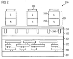
- a circuit arrangement 300 according to a third exemplary embodiment of the invention is described below with reference to FIG. 3 .
- Circuit arrangement 300 is on and in one Silicon chip 301 integrated.
- a holding element 302 which e.g. made of silicon oxide material on one Surface area of the silicon chip 301 cuboid four structures are formed according to the cantilever type kept floating.
- the holding element 302 can also be made of magnetic, especially permanent magnetic material be formed, but not free-floating but is attached to the silicon chip 302.
- the holding element 302 is wider, preferably much wider than the movable components 303a to 303d, 304a to 304d.
- Each of the structures is made up of one the spring element 303a to 303d coupled to the holding element 302 and one with the respective spring element 303a to 303d coupled permanent magnetic iron tongue 304a to 304d formed as a permanent magnet of a power supply unit.
- at least one respective structures 303a + 304a, 303b + 304b, 303c + 304c, 303d + 304d can be vibrated.
- each of the loops can be used 305a to 305d an induction voltage is generated, which by means of a respective rectifier 306 between the respective loop ends can be rectified, so that a sensor as a functional unit of the circuit arrangement 300 supplied with an electrical direct current can be.
- the free-floating Arrangements are provided, each consisting of one of the extending from the holding element 302
- Spring element strips 303a to 303d and one of the free end portion of a respective spring element strip 303a to 303d attached first to fourth iron tongue 304a to 304d are formed as a permanent magnet.
- Arrows 307 can be a stimulating external Vibration one or more of the assemblies from one Spring element 303a to 303d and an associated iron tongue 304a to 304d vibrate.
- this is permanent magnetic material of the energy supply unit not, as in Fig.1, in the form of a comb structure, but as iron tongues 304a to 304d provided separately from one another intended.
- Each of the tongues 304a to 304d swings over one associated meander loop 305a to 305d.
- the first to fourth spring elements 303a to 303d are narrower Part of the associated iron tongue 304a to 304d, which spring elements 303a to 303d laterally on the Holding element 302 are attached.
- the tongues 304a to 304d and the associated spring elements 303a to 303d respectively so configured that each of the assemblies 303a and 304a, 303b and 304b, 303c and 304c, and 303d and 304d at one predetermined frequency of a stimulating external vibration can swing optimally (i.e. in resonance).
- a wide frequency band of stimulating vibrations with the Circuit arrangement 300 are covered, with one external vibration of a certain vibration frequency or more of the tongues 304a to 304d together with the spring elements 303a to 303d resonates in vibration.
- all tongues 304a to 304d with a fixed Swing phase relationship to each other is for everyone Conductor loop 305a to 305d a separate rectifier 306 intended.
- each of tabs 304a through 304d has a thin one Extension, which serves as a spring element 303a to 303d.
- the respective resonance frequency of a Tongue-spring combination can be set.
- the Conductor loops 305a to 305d below tabs 304a to 304d can alternatively also be used as a spiral inductor or the like be carried out.
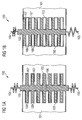
- Fig.4A to Fig.4D are different embodiments for the inductances of the circuit arrangement according to the invention shown.
- the coil shown in FIG. 4A is a spiral inductor in which a plurality of essentially rectangular turns are provided one inside the other.
- the spiral inductor from FIG. 4B is formed from essentially circular and concentric windings with a radius that increases from the inside to the outside.
- the spiral inductor from FIG. 4C differs from the spiral inductor from FIG. 4A in that it has conductor tracks with rounded edges.
- FIG. 4D shows an inductance in which three of the spiral inductors shown in FIG. 4A are connected together.
- Several of the inductors shown in FIGS. 4A, 4B and 4C can be interconnected in any combination in order to be able to obtain electrical energy from a vibrating permanent magnet particularly effectively.
- Such inductors can be arranged side by side and / or one above the other (that is also in two dimensions in the substrate plane), and also in a third dimension (that is to say a plurality of spiral inductor planes perpendicular to the drawing plane of FIG. 4D).
- a silicon oxide layer 502 with a thickness of approximately 100 nanometers is formed on a silicon substrate 501.
- a titanium nitride layer 503 with a thickness of approximately 10 nanometers to 100 nanometers is deposited on the silicon oxide layer 502.
- An additional titanium nitride layer 505 with a thickness of approximately 10 nanometers to 100 nanometers is deposited on the aluminum layer 504.
- the titanium nitride layer 503, the aluminum layer 504 and the additional titanium nitride layer 505 of the layer sequence 510 are structured using a lithography and an etching method in such a way that an integrated meander coil is thereby produced 511 is generated.
- Silicon nitride material (alternatively silicon oxide material or a low-k material) is deposited on the structured layer sequence and planarized using a CMP process ("chemical mechanical polishing"). This forms a silicon nitride region 512 in which the meander coil 511 is embedded. If a meander coil 511 is to be formed on the basis of copper material instead of aluminum material, this can be achieved using a damascene process.
- an etch stop layer 521 made of silicon nitride material is first deposited on the surface of the layer sequence 510, a sacrificial layer 522 made of silicon oxide material is deposited on the etch stop layer 521, and a magnetic layer 523 is deposited on the sacrificial layer 522 deposited from ferromagnetic iron material.
- the vertical extent of the magnetic layer 523 is approximately 200 nanometers.
- the magnetic layer 523 is first structured using a lithography and an etching method in such a way that first and second spring elements 532, 533 are formed, between which one iron comb structure 534 formed in a central region of the structured magnetic layer 523 is arranged.
- the sacrificial layer 522 below the region of the first and second spring elements 532, 533 and the iron comb structure 534 is subsequently removed using a selective etching process, so that material only in edge regions of the circuit arrangement 530 of the sacrificial layer 522 as a spacer 531 for maintaining a vertical distance between the etching stop layer 521 and the components of the magnetic layer 523 arranged above it.
- the etching stop layer 521 serves to stop the selective etching process, in which essentially only the material of the sacrificial layer 522 is etched, but not the material of the etching stop layer 521.
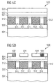
- FIGS. 6A to 6C Method of manufacturing a circuit arrangement according to described a fifth embodiment of the invention.
- the layer sequence 600 shown in FIG. 6A essentially corresponds to the layer sequence 520 shown in FIG. 5C. However, more individual components, that is to say coil turns of the meander coil 511, are provided in the layer sequence 600 than according to FIG. 5C.
- FIG. 6B shows a top view 610 of the circuit arrangement
- FIG. 6C shows a cross-sectional view 620 of the circuit arrangement, taken along a section line I-I 'shown in FIG. 6B.
- Fig. 6C is obtained using a lithographic and a The magnetic layer 523 of the layer sequence 600 structured in such a way that left and right edge regions of the structured magnetic layer 523 first and second holding areas 611, 612 are formed.
- a central area of the structured magnetic layer 523 is an iron comb structure 615 with a plurality of teeth 616 formed.
- a first spring element 613 is formed between the first holding area 611 and one 6B.
- a second Spring element 614 is formed between the 6B, Fig.6C right section of the iron comb structure 615 and the second holding area 612.
- Magnetic layer 523 After structuring the Magnetic layer 523 is made using an isotropic Etching process removes material from sacrificial layer 522 so that only in the left and right partial areas according to FIG. 6C the circuit arrangement between the etch stop layer 521 and the magnetic layer 523 are left with spacers 531.
- the meander coil is preferably according to one Damascene process trained.
- FIGS. 7A to 7E Shift sequences at different times during of a method for producing a circuit arrangement according to a sixth embodiment of the invention described for the meander coil made of copper material is formed.
- a first silicon oxide layer 701 is structured using a lithography and an etching method, and a barrier region 702 is formed in trenches formed in this way.
- the trench or trenches are subsequently filled with copper material, so that a first copper region 703 is formed by a planarization method (for example CMP method, "Chemical Mechanical Polishing").
- Silicon nitride material is deposited on the layer sequence thus obtained, whereby a first silicon nitride etch stop layer 704 is formed.
- a second silicon oxide layer 705 is formed on the layer sequence thus obtained.
- a second silicon nitride etch stop layer 706 is formed on the layer sequence thus obtained.
- An additional silicon oxide layer is deposited on the second silicon nitride etching stop layer 706 and structured using a lithography and an etching method to form a silicon oxide region 707, in which a trench 708 is introduced.
- an additional trench 711 is introduced into the second silicon oxide layer 705 and the second silicon nitride etching stop layer 706 using a lithography and an etching method.
- the additional trench 711 serves as a via opening.
- the first silicon nitride etching stop layer 704 serves to stop the etching process.
- a photomask (not shown) formed for structuring can be removed using an oxygen plasma method, for example.
- the first copper region 703 is protected against a negative influence by the oxygen plasma by means of the first silicon nitride etching stop layer 704.
- the layer sequence 710 is subjected to a selective etching process for removing exposed silicon nitride material, so that exposed silicon nitride material of the first and second silicon nitride etching stop layers 704, 706 is removed. As a result, copper material of the first copper region 703 is exposed. Due to overetching, the trench 708 now extends slightly into the second silicon oxide layer 705.
- material for forming a barrier layer 731 is applied to the layer sequence 720 using a sputtering method. Furthermore, in a two-stage process, a second copper region 732 is applied over the entire surface of the barrier layer 731. For this purpose, a thin seed layer is first deposited using a sputtering process, followed by depositing additional copper to form the second copper region 732 using an electroplating process.
- a CMP method (“Chemical Mechanical Polishing”) over the barrier layer 731, whereby a third copper region 741 is formed. Furthermore, silicon nitride material is deposited on the surface of the layer sequence thus obtained, whereby a protective layer 742 is obtained.
- At least part of the copper structure made up of first and third copper regions 703, 741 can be formed for example as a meander coil or a turn of the Meander coil can be used.
Landscapes
- Engineering & Computer Science (AREA)
- Power Engineering (AREA)
- Micromachines (AREA)
- Semiconductor Integrated Circuits (AREA)
Applications Claiming Priority (2)
| Application Number | Priority Date | Filing Date | Title |
|---|---|---|---|
| DE10310161A DE10310161B4 (de) | 2003-03-07 | 2003-03-07 | Monolithisch integrierte Schaltkreis-Anordnung |
| DE10310161 | 2003-03-07 |
Publications (3)
| Publication Number | Publication Date |
|---|---|
| EP1465327A2 true EP1465327A2 (fr) | 2004-10-06 |
| EP1465327A3 EP1465327A3 (fr) | 2004-10-13 |
| EP1465327B1 EP1465327B1 (fr) | 2008-05-07 |
Family
ID=32842148
Family Applications (1)
| Application Number | Title | Priority Date | Filing Date |
|---|---|---|---|
| EP04005329A Expired - Lifetime EP1465327B1 (fr) | 2003-03-07 | 2004-03-05 | Generateur à l'energie vibratoire et integré dans une substrat |
Country Status (4)
| Country | Link |
|---|---|
| US (1) | US7211909B2 (fr) |
| EP (1) | EP1465327B1 (fr) |
| JP (1) | JP4275550B2 (fr) |
| DE (2) | DE10310161B4 (fr) |
Families Citing this family (17)
| Publication number | Priority date | Publication date | Assignee | Title |
|---|---|---|---|---|
| US7142075B1 (en) * | 2004-04-01 | 2006-11-28 | Sandia Corporation | Microelectromechanical power generator and vibration sensor |
| US7289009B1 (en) | 2004-09-15 | 2007-10-30 | Sandia Corporation | Eddy-current-damped microelectromechanical switch |
| US7368312B1 (en) * | 2004-10-15 | 2008-05-06 | Morgan Research Corporation | MEMS sensor suite on a chip |
| KR100768919B1 (ko) * | 2004-12-23 | 2007-10-19 | 삼성전자주식회사 | 전원 생성 장치 |
| CN2877125Y (zh) * | 2005-08-12 | 2007-03-07 | 陈传生 | 震动式发电器 |
| EP1841049B1 (fr) * | 2006-03-28 | 2012-08-15 | Infineon Technologies AG | Micro-générateur électromagnétique |
| US20100052665A1 (en) * | 2007-02-01 | 2010-03-04 | Koninklijke Philips Electronics N.V. | Magnetic sensor device for and a method of sensing magnetic particles |
| US7759244B2 (en) * | 2007-05-10 | 2010-07-20 | United Microelectronics Corp. | Method for fabricating an inductor structure or a dual damascene structure |
| US20090160592A1 (en) * | 2007-12-20 | 2009-06-25 | Hopper Peter J | Helical core on-chip power inductor |
| US20100078216A1 (en) * | 2008-09-25 | 2010-04-01 | Baker Hughes Incorporated | Downhole vibration monitoring for reaming tools |
| US9048717B2 (en) * | 2009-09-16 | 2015-06-02 | Ecoharvester, Inc. | Multipolar electromagnetic generator |
| US8324998B2 (en) * | 2009-09-16 | 2012-12-04 | Ecoharvester, Inc. | Wireless switch with multipolar electromagnetic generator |
| DE102010042075A1 (de) * | 2010-03-31 | 2011-10-06 | Johnson Controls Gmbh | Vorrichtung zur Versorgung eines als Schlüsselanhänger ausgebildeten Fernbedienelementes einer Fahrzeugfernentriegelung mit elektrischer Energie |
| ES2677720T3 (es) * | 2013-03-11 | 2018-08-06 | Sts Spezial-Transformatoren-Stockach Gmbh & Co. Kg | Componente inductivo |
| US9557306B2 (en) * | 2013-12-20 | 2017-01-31 | Honeywell International Inc. | Magnetically controlled gas detectors |
| US9923545B2 (en) | 2014-10-22 | 2018-03-20 | Microchip Technology Incorporated | Compound spring MEMS resonators for frequency and timing generation |
| US9866200B2 (en) * | 2014-10-22 | 2018-01-09 | Microchip Technology Incorporated | Multiple coil spring MEMS resonator |
Family Cites Families (4)
| Publication number | Priority date | Publication date | Assignee | Title |
|---|---|---|---|---|
| US4857893A (en) * | 1986-07-18 | 1989-08-15 | Bi Inc. | Single chip transponder device |
| US6475639B2 (en) * | 1996-01-18 | 2002-11-05 | Mohsen Shahinpoor | Ionic polymer sensors and actuators |
| US6332359B1 (en) * | 1997-04-24 | 2001-12-25 | Fuji Electric Co., Ltd. | Semiconductor sensor chip and method for producing the chip, and semiconductor sensor and package for assembling the sensor |
| US7357197B2 (en) * | 2000-11-07 | 2008-04-15 | Halliburton Energy Services, Inc. | Method and apparatus for monitoring the condition of a downhole drill bit, and communicating the condition to the surface |
-
2003
- 2003-03-07 DE DE10310161A patent/DE10310161B4/de not_active Expired - Fee Related
-
2004
- 2004-03-05 EP EP04005329A patent/EP1465327B1/fr not_active Expired - Lifetime
- 2004-03-05 DE DE502004007025T patent/DE502004007025D1/de not_active Expired - Lifetime
- 2004-03-05 US US10/794,588 patent/US7211909B2/en not_active Expired - Fee Related
- 2004-03-08 JP JP2004063836A patent/JP4275550B2/ja not_active Expired - Lifetime
Non-Patent Citations (5)
| Title |
|---|
| LI W J ET AL: "Infrared signal transmission by a laser-micromachined vibration-induced power generator" PROCEEDINGS 43RD IEEE MIDWEST SYMPOSIUM ON CIRCUITS AND SYSTEMS, Bd. 1, 8. August 2000 (2000-08-08), Seiten 236-239, XP010558118 * |
| MENINGER S ET AL: "Vibration-to-electric energy conversion" PROCEEDINGS 1999 INTERNATIONAL SYMPOSIUM ON LOW POWER ELECTRONICS AND DESIGN. (ISLPED). SAN DIEGO, CA, AUG. 16 - 17, 1999, INTERNATIONAL SYMPOSIUM ON LOW POWER ELECTRONICS AND DESIGN, NEW YORK, NY : ACM, US, 16. August 1999 (1999-08-16), Seiten 48-53, XP010355950 ISBN: 1-58113-133-X * |
| T.M.LIAKOPOULOS, W. ZHANG, C.H.AHN: "Micromashined thick permanent magnet arrays on silicon wafers" IEEE TRANSACTIONS ON MAGNETICS, Nr. 5, September 1996 (1996-09), Seiten 5154-5156, XP002292024 * |
| WAGNER B ET AL: "Microfabricated actuator with moving permanent magnet" PROCEEDINGS OF THE WORKSHOP ON MICRO ELECTRO MECHANICAL SYSTEMS. INVESTIGATION OF MICRO STRUCTURES, SENSORS, ACTUATORS, MACHINES AND ROBOTS. NARA, JP., JAN. 30 - FEB. 2, 1991, NEW YORK, IEEE, US, Bd. WORKSHOP 4, 30. Januar 1991 (1991-01-30), Seiten 27-32, XP010039601 ISBN: 0-87942-641-1 * |
| WILLIAMS C B ET AL: "Development of an electromagnetic micro-generator" IEE PROCEEDINGS: CIRCUITS DEVICES AND SYSTEMS, INSTITUTION OF ELECTRICAL ENGINEERS, STENVENAGE, GB, Bd. 148, Nr. 6, 5. Dezember 2001 (2001-12-05), Seiten 337-342, XP006017626 ISSN: 1350-2409 * |
Also Published As
| Publication number | Publication date |
|---|---|
| EP1465327B1 (fr) | 2008-05-07 |
| US7211909B2 (en) | 2007-05-01 |
| JP4275550B2 (ja) | 2009-06-10 |
| EP1465327A3 (fr) | 2004-10-13 |
| US20040246647A1 (en) | 2004-12-09 |
| DE502004007025D1 (de) | 2008-06-19 |
| DE10310161A1 (de) | 2004-09-23 |
| DE10310161B4 (de) | 2009-04-09 |
| JP2004297050A (ja) | 2004-10-21 |
Similar Documents
| Publication | Publication Date | Title |
|---|---|---|
| EP1465327B1 (fr) | Generateur à l'energie vibratoire et integré dans une substrat | |
| US8928162B2 (en) | Sensor with energy-harvesting device | |
| JP4813739B2 (ja) | フォトリソグラフィックパターン形成による立体コイル構造 | |
| US7608975B2 (en) | Piezoelectrically-controlled integrated magnetic device | |
| EP1441234B1 (fr) | Sonde à noyau saturable, intégrée dans un substrat semiconducteur et procédé de fabrication | |
| US20090181473A1 (en) | Magnetically enhanced power inductor with self-aligned hard axis magnetic core produced in an applied magnetic field using a damascene process sequence | |
| DE112013000325T5 (de) | Architektur und Herstellung von induktiven Inertialsensoren in Verpackungsaufbauschichten | |
| US20170141668A1 (en) | Chip-scale electromagnetic vibrational energy harvester | |
| EP2467727B1 (fr) | Capteur de champ magnétique et procédé de production d'un capteur de champ magnétique | |
| Miki et al. | Electromagnetic energy harvester by using buried NdFeB | |
| EP1484618B1 (fr) | Sonde à noyau saturable miniature et son procédé de fabrication | |
| EP1841049B1 (fr) | Micro-générateur électromagnétique | |
| US7397326B2 (en) | Electromechanical filter | |
| DE102007030744A1 (de) | Magnetorestriktiver Mikrolautsprecher | |
| Krishnapriya et al. | Design and analysis of non-spiral planar microcoil-based electromagnetic microactuator | |
| WO2008148413A1 (fr) | Micro-solénoïdes et micro-transformateurs enroulés | |
| Zhou et al. | Magnetoelectric current sensor | |
| DE102012205268A1 (de) | Verfahren zum Herstellen von zumindest einer Kontaktierungsfläche eines Bauelementes und Sensor zum Aufnehmen einer Richtungskomponente einer gerichteten Messgröße | |
| AU6052498A (en) | Vialess integrated inductive elements for electromagnetic applications | |
| Shirai et al. | Electromagnetic energy harvester with high efficiency using micro-machining Si springs | |
| Tien | Tunable RF mems elements | |
| DE102006040726A1 (de) | Vorrichtung zur Energieumwandlung, insbesondere piezoelektrischer Mikro-Power-Wandler | |
| WO2008025789A1 (fr) | Dispositif doté d'un convertisseur capacitif intégré sur un substrat | |
| Soft magnetic materials and devices on energy applications | ||
| DE102011082320A1 (de) | Mikro-elektromechanischer Magnetfeldsensor und Verfahren zum Erfassen eines Magnetfelds |
Legal Events
| Date | Code | Title | Description |
|---|---|---|---|
| PUAI | Public reference made under article 153(3) epc to a published international application that has entered the european phase |
Free format text: ORIGINAL CODE: 0009012 |
|
| PUAL | Search report despatched |
Free format text: ORIGINAL CODE: 0009013 |
|
| AK | Designated contracting states |
Kind code of ref document: A2 Designated state(s): AT BE BG CH CY CZ DE DK EE ES FI FR GB GR HU IE IT LI LU MC NL PL PT RO SE SI SK TR |
|
| AX | Request for extension of the european patent |
Extension state: AL LT LV MK |
|
| AK | Designated contracting states |
Kind code of ref document: A3 Designated state(s): AT BE BG CH CY CZ DE DK EE ES FI FR GB GR HU IE IT LI LU MC NL PL PT RO SE SI SK TR |
|
| AX | Request for extension of the european patent |
Extension state: AL LT LV MK |
|
| 17P | Request for examination filed |
Effective date: 20041104 |
|
| 17Q | First examination report despatched |
Effective date: 20050421 |
|
| AKX | Designation fees paid |
Designated state(s): DE |
|
| GRAP | Despatch of communication of intention to grant a patent |
Free format text: ORIGINAL CODE: EPIDOSNIGR1 |
|
| GRAS | Grant fee paid |
Free format text: ORIGINAL CODE: EPIDOSNIGR3 |
|
| GRAA | (expected) grant |
Free format text: ORIGINAL CODE: 0009210 |
|
| AK | Designated contracting states |
Kind code of ref document: B1 Designated state(s): DE |
|
| REF | Corresponds to: |
Ref document number: 502004007025 Country of ref document: DE Date of ref document: 20080619 Kind code of ref document: P |
|
| PLBE | No opposition filed within time limit |
Free format text: ORIGINAL CODE: 0009261 |
|
| STAA | Information on the status of an ep patent application or granted ep patent |
Free format text: STATUS: NO OPPOSITION FILED WITHIN TIME LIMIT |
|
| 26N | No opposition filed |
Effective date: 20090210 |
|
| PGFP | Annual fee paid to national office [announced via postgrant information from national office to epo] |
Ref country code: DE Payment date: 20120515 Year of fee payment: 9 |
|
| REG | Reference to a national code |
Ref country code: DE Ref legal event code: R119 Ref document number: 502004007025 Country of ref document: DE Effective date: 20131001 |
|
| PG25 | Lapsed in a contracting state [announced via postgrant information from national office to epo] |
Ref country code: DE Free format text: LAPSE BECAUSE OF NON-PAYMENT OF DUE FEES Effective date: 20131001 |