EP1465253A2 - Semiconductor package and lead frame therefor - Google Patents
Semiconductor package and lead frame therefor Download PDFInfo
- Publication number
- EP1465253A2 EP1465253A2 EP04007816A EP04007816A EP1465253A2 EP 1465253 A2 EP1465253 A2 EP 1465253A2 EP 04007816 A EP04007816 A EP 04007816A EP 04007816 A EP04007816 A EP 04007816A EP 1465253 A2 EP1465253 A2 EP 1465253A2
- Authority
- EP
- European Patent Office
- Prior art keywords
- leads
- lead
- lead frame
- stage
- semiconductor package
- Prior art date
- Legal status (The legal status is an assumption and is not a legal conclusion. Google has not performed a legal analysis and makes no representation as to the accuracy of the status listed.)
- Withdrawn
Links
Images




Classifications
-
- H—ELECTRICITY
- H10—SEMICONDUCTOR DEVICES; ELECTRIC SOLID-STATE DEVICES NOT OTHERWISE PROVIDED FOR
- H10W—GENERIC PACKAGES, INTERCONNECTIONS, CONNECTORS OR OTHER CONSTRUCTIONAL DETAILS OF DEVICES COVERED BY CLASS H10
- H10W70/00—Package substrates; Interposers; Redistribution layers [RDL]
- H10W70/40—Leadframes
- H10W70/421—Shapes or dispositions
- H10W70/424—Cross-sectional shapes
-
- A—HUMAN NECESSITIES
- A61—MEDICAL OR VETERINARY SCIENCE; HYGIENE
- A61H—PHYSICAL THERAPY APPARATUS, e.g. DEVICES FOR LOCATING OR STIMULATING REFLEX POINTS IN THE BODY; ARTIFICIAL RESPIRATION; MASSAGE; BATHING DEVICES FOR SPECIAL THERAPEUTIC OR HYGIENIC PURPOSES OR SPECIFIC PARTS OF THE BODY
- A61H3/00—Appliances for aiding patients or disabled persons to walk about
- A61H3/04—Wheeled walking aids for patients or disabled persons
-
- H—ELECTRICITY
- H10—SEMICONDUCTOR DEVICES; ELECTRIC SOLID-STATE DEVICES NOT OTHERWISE PROVIDED FOR
- H10W—GENERIC PACKAGES, INTERCONNECTIONS, CONNECTORS OR OTHER CONSTRUCTIONAL DETAILS OF DEVICES COVERED BY CLASS H10
- H10W70/00—Package substrates; Interposers; Redistribution layers [RDL]
- H10W70/40—Leadframes
- H10W70/421—Shapes or dispositions
-
- H—ELECTRICITY
- H10—SEMICONDUCTOR DEVICES; ELECTRIC SOLID-STATE DEVICES NOT OTHERWISE PROVIDED FOR
- H10W—GENERIC PACKAGES, INTERCONNECTIONS, CONNECTORS OR OTHER CONSTRUCTIONAL DETAILS OF DEVICES COVERED BY CLASS H10
- H10W70/00—Package substrates; Interposers; Redistribution layers [RDL]
- H10W70/40—Leadframes
- H10W70/456—Materials
- H10W70/457—Materials of metallic layers on leadframes
-
- H—ELECTRICITY
- H10—SEMICONDUCTOR DEVICES; ELECTRIC SOLID-STATE DEVICES NOT OTHERWISE PROVIDED FOR
- H10W—GENERIC PACKAGES, INTERCONNECTIONS, CONNECTORS OR OTHER CONSTRUCTIONAL DETAILS OF DEVICES COVERED BY CLASS H10
- H10W74/00—Encapsulations, e.g. protective coatings
- H10W74/10—Encapsulations, e.g. protective coatings characterised by their shape or disposition
- H10W74/111—Encapsulations, e.g. protective coatings characterised by their shape or disposition the semiconductor body being completely enclosed
-
- A—HUMAN NECESSITIES
- A61—MEDICAL OR VETERINARY SCIENCE; HYGIENE
- A61H—PHYSICAL THERAPY APPARATUS, e.g. DEVICES FOR LOCATING OR STIMULATING REFLEX POINTS IN THE BODY; ARTIFICIAL RESPIRATION; MASSAGE; BATHING DEVICES FOR SPECIAL THERAPEUTIC OR HYGIENIC PURPOSES OR SPECIFIC PARTS OF THE BODY
- A61H3/00—Appliances for aiding patients or disabled persons to walk about
- A61H3/04—Wheeled walking aids for patients or disabled persons
- A61H2003/046—Wheeled walking aids for patients or disabled persons with braking means
-
- A—HUMAN NECESSITIES
- A61—MEDICAL OR VETERINARY SCIENCE; HYGIENE
- A61H—PHYSICAL THERAPY APPARATUS, e.g. DEVICES FOR LOCATING OR STIMULATING REFLEX POINTS IN THE BODY; ARTIFICIAL RESPIRATION; MASSAGE; BATHING DEVICES FOR SPECIAL THERAPEUTIC OR HYGIENIC PURPOSES OR SPECIFIC PARTS OF THE BODY
- A61H2201/00—Characteristics of apparatus not provided for in the preceding codes
- A61H2201/01—Constructive details
- A61H2201/0119—Support for the device
- A61H2201/0138—Support for the device incorporated in furniture
- A61H2201/0149—Seat or chair
-
- H—ELECTRICITY
- H05—ELECTRIC TECHNIQUES NOT OTHERWISE PROVIDED FOR
- H05K—PRINTED CIRCUITS; CASINGS OR CONSTRUCTIONAL DETAILS OF ELECTRIC APPARATUS; MANUFACTURE OF ASSEMBLAGES OF ELECTRICAL COMPONENTS
- H05K3/00—Apparatus or processes for manufacturing printed circuits
- H05K3/30—Assembling printed circuits with electric components, e.g. with resistors
- H05K3/32—Assembling printed circuits with electric components, e.g. with resistors electrically connecting electric components or wires to printed circuits
- H05K3/34—Assembling printed circuits with electric components, e.g. with resistors electrically connecting electric components or wires to printed circuits by soldering
- H05K3/341—Surface mounted components
- H05K3/3421—Leaded components
- H05K3/3426—Leaded components characterised by the leads
-
- H—ELECTRICITY
- H10—SEMICONDUCTOR DEVICES; ELECTRIC SOLID-STATE DEVICES NOT OTHERWISE PROVIDED FOR
- H10W—GENERIC PACKAGES, INTERCONNECTIONS, CONNECTORS OR OTHER CONSTRUCTIONAL DETAILS OF DEVICES COVERED BY CLASS H10
- H10W72/00—Interconnections or connectors in packages
- H10W72/50—Bond wires
- H10W72/551—Materials of bond wires
- H10W72/552—Materials of bond wires comprising metals or metalloids, e.g. silver
-
- H—ELECTRICITY
- H10—SEMICONDUCTOR DEVICES; ELECTRIC SOLID-STATE DEVICES NOT OTHERWISE PROVIDED FOR
- H10W—GENERIC PACKAGES, INTERCONNECTIONS, CONNECTORS OR OTHER CONSTRUCTIONAL DETAILS OF DEVICES COVERED BY CLASS H10
- H10W74/00—Encapsulations, e.g. protective coatings
-
- H—ELECTRICITY
- H10—SEMICONDUCTOR DEVICES; ELECTRIC SOLID-STATE DEVICES NOT OTHERWISE PROVIDED FOR
- H10W—GENERIC PACKAGES, INTERCONNECTIONS, CONNECTORS OR OTHER CONSTRUCTIONAL DETAILS OF DEVICES COVERED BY CLASS H10
- H10W90/00—Package configurations
- H10W90/701—Package configurations characterised by the relative positions of pads or connectors relative to package parts
- H10W90/751—Package configurations characterised by the relative positions of pads or connectors relative to package parts of bond wires
- H10W90/756—Package configurations characterised by the relative positions of pads or connectors relative to package parts of bond wires between a chip and a stacked lead frame, conducting package substrate or heat sink
Definitions
- This invention relates to semiconductor packages for mounting semiconductor chips using lead frames, which are attached onto circuit boards. This invention also relates to methods for manufacturing semiconductor packages using lead frames.
- leads frames are used for semiconductor packages incorporating semiconductor chips.
- a typical example of the lead frame for use in the conventionally-known semiconductor package is shown in FIG. 13, wherein a lead frame 51 comprises a stage 55 for mounting a semiconductor chip 53, a plurality of leads 57 arranged in the periphery of the stage 55, and dam bars 59 for interconnecting the leads 57.
- This lead frame 51 is manufactured by performing press working or etching process on a thin metal plate.
- the aforementioned lead frame 51 can be used for manufacturing the conventionally-known semiconductor package of a QFN type (i.e., a Quad Flat Non-Leaded package), for example.
- the semiconductor chip 53 is bonded onto the surface of the stage 55, wherein pads thereof are electrically connected with the leads 57 via bonding wires 61.
- a molded resin 63 is formed to integrally fix the semiconductor chip 53, the stage 55, the bonding wire 61, and the bonding portion of the lead 57 together.
- a backside 57a of the lead 57 forms the same plane together with a backside 63a of the molded resin 63.
- a prescribed surface 57b of the lead 57 is exposed to the exterior of the molded resin 63 and is subjected to plating together with the backside 57a of the lead 57, whereby plated films 65 are formed thereon in order to improve solder wettability with respect to the lead 57.
- a projecting portion 57c of the lead 57 which projects outwardly from the molded resin 63, is cut out together with a dam bar 59 at a cutting line A, so that the leads 57 are made electrically independent of each other, thus completing the production of the semiconductor package.
- the conventionally-known package of a QFP type (i.e., a Quad FlatPack package) is designed such that plated films are formed on the surface and backside of the projecting portion of the lead as well as the adjacent side areas of the leads in order to improve the wettability, wherein the solder is adhered not only to the backside of the lead but also to the side area and surface of the lead.
- the projecting portion of the lead is subjected to half etching so as to form a thinned portion, thus increasing the overall solder adhesion area of the lead, an example of which is disclosed in Japanese Patent No. 3008470.
- the lead 57 is cut out at the cutting line A, whereby a cut surface 57d of the lead 57 lying in the thickness direction is not accompanied with a plating film 65 as shown in FIG. 15, whereas other surfaces of the lead 57 except the cut surface 57d are covered with the molded resin 63 so that they do not join with a solder 67. That is, when a semiconductor package 80 is attached onto a circuit board 71 via the solder 67 as shown in FIG. 15, only a land portion 73 of the circuit board 71 is electrically connected with the backside 57a of the lead 57. This causes difficulty in inspecting the joined state established between the solder 67 and the lead 57 through visual inspection. Hence, there is a problem in that reliability secured for the electrical connection established between the semiconductor package 80 and the circuit board 71 may be reduced.
- the aforementioned Japanese patent discloses a method for increasing the overall solder adhesion area with respect to the leads.
- this method cannot contribute to enhancement of the joining strength established between the cut surface 57d of the lead and the solder 67; that is, it cannot solve the aforementioned problem.
- a lead frame which is produced by processing a thin metal plate, comprises a stage for mounting a semiconductor chip, a plurality of leads arranged in the periphery of the stage, and lead interconnection members (e.g., dam bars) for interconnecting the leads, wherein a through hole is formed in the thickness direction of the lead frame with respect to each of the leads or each of the lead interconnection members.
- lead interconnection members e.g., dam bars
- the lead and its associated portion are subjecting to cutting along a cutting line that is set to pass through the through hole, whereby the leads are made electrically independent of each other.
- the leads and/or the lead interconnection members are subjected to cutting, whereby a plated film reliably remains in the interior wall of the through hole that forms the side surface of the lead in its thickness direction. That is, it is possible to increase the overall solder adhesion area with respect to the leads, which can be therefore improved in the joining strength with the solder.
- the lead frame in which a relatively small through hole is formed with respect to each of the leads is advantageous because the overall plated area can be increased with respect to the side surfaces of the leads after the lead interconnection members are cut out, and hence, it is possible to easily increase the overall solder adhesion area with respect to the leads.
- a manufacturing method for a semiconductor package is characterized by comprising a lead frame forming step for forming a lead frame by processing a thin metal plate so as to provide a stage, a plurality of leads arranged in the periphery of the stage, and a plurality of lead interconnection members (e.g., dam bars) for interconnecting the leads; a chip mounting step for bonding a semiconductor chip onto the stage of the lead frame and for wiring the semiconductor chip with the leads; a molding step for forming a molded resin for integrally fixing the stage, semiconductor chip, and leads therein; a plating step for performing plating on prescribed surfaces of the leads that are exposed to the exterior of the molded resin; and a cutting step for cutting the leads at a cutting line (or cutting lines) so that the leads are made electrically independent of each other.
- a lead frame forming step for forming a lead frame by processing a thin metal plate so as to provide a stage, a plurality of leads arranged in the periphery of the stage, and
- a through hole forming step which is performed at the appropriate timing in the time period between the lead frame forming step and the plating step, for forming a through hole penetrating through the lead frame in its thickness direction and allowing the cutting line to pass therethrough with respect to each of the leads.
- the through hole can be elongated and is formed in each of the lead interconnection members across the leads so as to allow the cutting lines to pass therethrough.
- the leads are partially exposed to the exterior of the molded resin, wherein the side surface of the exposed portion of the lead in its thickness direction provides a plated surface and a cut surface that adjoins the plated surface and that makes the adjoining leads to be electrically independent of each other. Due to the formation of the plated surface on the side surface of the lead exposed from the molded resin, it is possible to increase the solder adhesion area with respect to the lead, which is thus improved in the joining strength with the solder.
- the 'plated' backside of the lead adjacent to the plated surface on the side surface of the lead forms the same plane together with the lower surface of the molded resin, whereby when the semiconductor package is mounted on the circuit board in such a way that the lower surface is placed opposite to the surface of the circuit board, it is possible to reduce the height dimensions of the semiconductor package measured from the surface of the circuit board; in short, it is possible to reduce the thickness dimensions of the semiconductor package.
- FIGS. 1, 2, 3A, and 3B The outline of a manufacturing method for a semiconductor package according to a preferred embodiment of the invention will be described with reference to FIGS. 1, 2, 3A, and 3B.
- a thin metal plate made of copper and the like is subjected to one of or both of press working and etching process, thus producing a lead frame 1 (see FIG. 1) comprising a stage 5 for mounting a semiconductor chip 3, a plurality of leads 7 arranged in the periphery of the stage 5, and dam bars (i.e., lead interconnecting members) for interconnecting the leads 7.
- a plurality of through holes 17 penetrating through the lead frame 1 are simultaneously formed with respect to the leads 7 respectively due to the press working and/or the etching process, wherein the through holes 17 are aligned along with the arrangements of the leads 7.
- the semiconductor chip 3 is bonded onto a surface 5a of the stage 5; then, pads of the semiconductor chip 3 are electrically connected with the leads 7 respectively via metal bonding wires 11.
- the bonding position of the lead 7 bonded with the bonding wire 11 is located on a prescribed surface 7a of the lead 7, which is shifted inwardly in position from the through hole 17 towards the stage 5.
- the aforementioned lead frame 1 is arranged in a metal mold (not shown), into which a melted resin is injected so as to form a molded resin 13 (see FIG. 2) that integrally fixes the semiconductor chip 3, the stage 5, the bonding wire 11, and the bonding portion of the lead 7 at prescribed positions.
- a backside 13a of the molded resin 13 forms the same plane together with a backside 7b of the lead 7, wherein a prescribed side surface of the molded resin 13 in its thickness direction lies along a cutting line A for the lead, which will be described later. That is, the prescribed side surface of the molded resin 13 lies at a prescribed position at which the overall length of the through hole 17, which is formed in a longitudinal direction (i.e., C-D directions) of the lead 7, is reduced to a half.
- the molded resin 13 is formed to prevent a resin from being introduced into the through hole 17.
- a semiconductor package 30 of a QFN type as shown in FIG. 3A, wherein the lead 7 is not projected outside of a prescribed side surface 13b of the molded resin 13.
- a side surface 7d of the lead 7 in its thickness direction (see FIG. 3B) that is exposed outwardly is formed by cutting the lead 7 at the cutting line A.
- the side surface 7d of the lead 7 comprises a cut surface 7e, which forms the same plane as the side surface 13b of the molded resin 13, and a concave portion (or a plated surface) 7f that forms a part of an interior wall 17a of the through hole 17, wherein a plated film 15 is formed on the concave portion 7f.
- the lead frame 1 is formed in such a way that the through holes 17 are formed with respect to the leads 7; then, it is subjected to plating. Hence, by cutting each of the leads 7 at the cutting line A, it is possible to easily produce the semiconductor package 30 in which the plated film 15 is formed on the concave portion 7f of the side surface 7d of the lead 7.
- the plated films 15 on the concave portion 7f of the side surface 7d forming the tip end of the lead 7 as well as the backside 7b of the lead 7, it is possible to noticeably improve wettability, and it is possible to increase the overall adhesion area of the solder 25 with respect to the lead 7; hence, it is possible to noticeably improve the joining strength established between the lead 7 and the solder 25.
- the plated film 15 formed on the concave portion 7f is exposed outwardly and upwardly, which makes it easy for a human inspector to perform visual inspection on the joined state between the lead 7 and the solder 25. Therefore, it is possible to improve the reliability in establishing electrical connection between the lead 7 and the land portion 23 of the circuit board 21 when the semiconductor package 30 is attached onto the circuit board 21.
- the aforementioned semiconductor package 30 is advantageous in that it is possible to reduce height dimensions measured from the surface of the circuit board 21 when the semiconductor package 30 is attached onto the circuit board 21 because the backside 7b of the lead 7 forms the same plane together with the lower surface 13a of the molded resin 13. In short, it is possible to noticeably reduce the overall thickness of the semiconductor package 30.
- the present embodiment is designed such that the cut surface 7e of the lead 7 is located in the same plane of the side surface 13b of the molded resin 13.
- this invention is not necessarily limited to the present embodiment, which can be modified such that as shown in FIG. 4, the tip end of the lead 7 is partially projected outside of the side surface 13b of the molded resin 13. In this case, the plated film 15 can remain on the surface 7a of the lead 7 that is exposed to the exterior of the molded resin 13.
- the through hole 17 should be formed outwardly from the side surface 13b of the molded resin 13 as shown in FIG. 5.
- the through hole 17 should be enlarged in dimensions in a direction as it separates off from the side surface 13b of the molded resin 13.
- the present embodiment is designed such that the lead 7 is subjected to cutting at a prescribed cutting position at which the length of the through hole 17 lying in the longitudinal direction of the lead 7 is reduced to a half.
- this invention is not necessarily limited to the present embodiment, which can be modified such that the cutting position can be set at any position of the through hole 17.
- the through hole 17 is not necessarily formed with respect to each lead 7. That is, the through hole 17 can be formed at a prescribed position of the dam bar 9 interconnecting the leads 7.
- an elongated through hole 18 is formed in an alignment direction of leads 6 across a plurality of the leads 6, wherein the leads 6 including the interior wall of the through hole 18 and the dam bar 9 are subjected to plating; then, the dam bar 9 is subjected to cutting at cutting lines B.
- the leads 6 are made electrically independent of each other.
- each of side surfaces 6a of the leads 6 in their thickness directions is constituted by a plated surface 6f forming the tip end of the lead 6 on which a plated film 15 is formed, and a cut surface 6d that adjoins the plated surface 6f and is positioned opposite to the other adjacent lead 6, wherein a prescribed surface 6b adjoining the side surface 6a of the lead 6 is subjected to plating as well.
- the aforementioned semiconductor package 31 is characterized by forming a relatively large through hole 18, which is larger than the foregoing through hole 17 formed with respect to each lead 7; hence, it is possible to easily increase the total area of the plated surface 6f of the lead 6. Thus, it is possible to reliably improve the joining strength between the solder and the lead 6 by further increasing the solder adhesion area with respect to the lead 6.
- each of the leads 6 has a projecting portion 6b, which is projected inside of the through hole 18 in the longitudinal direction (i.e., a direction E) thereof, wherein a further projecting portion 6c is formed from the projecting portion 6b of the lead 6.
- the overall area of the plated surface 6f is not necessarily increased by forming the further projecting portion 6c further projected inside of the through hole 18. Instead, it is possible to form a hollow (or a recess) at the projecting portion 6b forming the tip end of the lead 6.
- the through hole 18 is formed across a plurality of leads 6 in the alignment direction of the leads 6, which is not restricted in this invention. That is, this invention requires that a through hole be formed at the prescribed position allowing the cutting line to pass therethrough in order to make the adjacent leads 6 electrically independent of each other. For instance, it is possible to form a through hole on the cutting line B passing between the adjacent leads 6.
- the through hole(s) is formed simultaneously with the formation of the lead frame, which is not restricted in this invention. That is, this invention requires that the through hole be formed within a time period between the formation of the lead frame and the timing to perform plating. Specifically, the through holes can be formed simultaneously with the formation of the molded resin 13. Due to the provision of the through hole(s), it is possible to increase the overall area for the plating, and it is possible to reduce the overall cutting area for making the leads electrically independent of each other. It is therefore possible to provide an effect in which the semiconductor package can be produced with ease.
- the plated surface 6f and the concave portions 7f and 8f, which are subjected to plating, are formed in the thickness directions of the leads 6-8, which is not restricted in this invention.
- the present embodiment can be modified as shown in FIG. 9 such that a part of a side surface 10d of a lead 10 located in proximity to a backside 10b is subjected to plating, thus forming a plated surface 10f.
- the solder 25 can join the plated surface 10f in addition to the backside 10b of the lead 10; therefore, it is possible to improve the reliability in establishing the electrical connection between the lead 10 and the land portion 23 of the circuit board 21.
- the semiconductor package 32 can be modified as shown in FIG. 10 such that instead of forming the foregoing through holes 17 and 18 penetrating through the lead frame, a hollow portion 12 should be formed by etching or machining on the backside 10b of the lead 10 in association with the cutting line A, which is set to make the adjacent leads 10 electrically independent of each other.
- an interior wall 12a of the hollow portion 12 is subjected to plating, thus forming the aforementioned plated surface 10f.
- Each of the aforementioned semiconductor packages 30-32 is constituted as the QFN type, which is not restricted in this invention when the semiconductor package is not necessarily reduced in thickness. That is, each of them can be constituted as the QFP type providing the aforementioned leads 8, which are projected outside of the molded resin 13.
- the aforementioned semiconductor package as shown in FIG. 11 it is possible to partially modify the aforementioned semiconductor package as shown in FIG. 11 such that the through hole 17 is formed on a joining portion 8a of the lead 8 joining the solder 25, wherein the interior wall 17a of the through hole 17 is subjected to plating; then, the lead 8 is subjected to cutting at a cutting line A.
- FIG. 11 it is possible to produce a semiconductor package as shown in FIG.
Landscapes
- Health & Medical Sciences (AREA)
- Epidemiology (AREA)
- Pain & Pain Management (AREA)
- Physical Education & Sports Medicine (AREA)
- Rehabilitation Therapy (AREA)
- Life Sciences & Earth Sciences (AREA)
- Animal Behavior & Ethology (AREA)
- General Health & Medical Sciences (AREA)
- Public Health (AREA)
- Veterinary Medicine (AREA)
- Lead Frames For Integrated Circuits (AREA)
- Structures Or Materials For Encapsulating Or Coating Semiconductor Devices Or Solid State Devices (AREA)
Abstract
Description
- This invention relates to semiconductor packages for mounting semiconductor chips using lead frames, which are attached onto circuit boards. This invention also relates to methods for manufacturing semiconductor packages using lead frames.
- This application claims priority on Japanese Patent Application No. 2003-99126 and Japanese Patent Application (not yet assigned a number, which claims priority on Japanese Patent Application No. 2003-99126 in Japan), the contents of which are incorporated herein by reference.
- Conventionally, leads frames are used for semiconductor packages incorporating semiconductor chips. A typical example of the lead frame for use in the conventionally-known semiconductor package is shown in FIG. 13, wherein a
lead frame 51 comprises astage 55 for mounting asemiconductor chip 53, a plurality ofleads 57 arranged in the periphery of thestage 55, anddam bars 59 for interconnecting theleads 57. Thislead frame 51 is manufactured by performing press working or etching process on a thin metal plate. - The
aforementioned lead frame 51 can be used for manufacturing the conventionally-known semiconductor package of a QFN type (i.e., a Quad Flat Non-Leaded package), for example. In this case, thesemiconductor chip 53 is bonded onto the surface of thestage 55, wherein pads thereof are electrically connected with theleads 57 viabonding wires 61. Then, as shown in FIG. 14, a moldedresin 63 is formed to integrally fix thesemiconductor chip 53, thestage 55, thebonding wire 61, and the bonding portion of thelead 57 together. Herein, abackside 57a of thelead 57 forms the same plane together with abackside 63a of the moldedresin 63. - A prescribed
surface 57b of thelead 57 is exposed to the exterior of the moldedresin 63 and is subjected to plating together with thebackside 57a of thelead 57, wherebyplated films 65 are formed thereon in order to improve solder wettability with respect to thelead 57. - Thereafter, a projecting
portion 57c of thelead 57, which projects outwardly from themolded resin 63, is cut out together with adam bar 59 at a cutting line A, so that theleads 57 are made electrically independent of each other, thus completing the production of the semiconductor package. - The conventionally-known package of a QFP type (i.e., a Quad FlatPack package) is designed such that plated films are formed on the surface and backside of the projecting portion of the lead as well as the adjacent side areas of the leads in order to improve the wettability, wherein the solder is adhered not only to the backside of the lead but also to the side area and surface of the lead.
- In the QFP package, the projecting portion of the lead is subjected to half etching so as to form a thinned portion, thus increasing the overall solder adhesion area of the lead, an example of which is disclosed in Japanese Patent No. 3008470.
- In the QFN package shown in FIG. 14, the
lead 57 is cut out at the cutting line A, whereby acut surface 57d of thelead 57 lying in the thickness direction is not accompanied with aplating film 65 as shown in FIG. 15, whereas other surfaces of thelead 57 except thecut surface 57d are covered with themolded resin 63 so that they do not join with asolder 67. That is, when asemiconductor package 80 is attached onto acircuit board 71 via thesolder 67 as shown in FIG. 15, only aland portion 73 of thecircuit board 71 is electrically connected with thebackside 57a of thelead 57. This causes difficulty in inspecting the joined state established between thesolder 67 and thelead 57 through visual inspection. Hence, there is a problem in that reliability secured for the electrical connection established between thesemiconductor package 80 and thecircuit board 71 may be reduced. - The aforementioned Japanese patent discloses a method for increasing the overall solder adhesion area with respect to the leads. However, in the QFN package in which the
lead 57 is not substantially projected outside of themolded resin 63 so that the other surfaces of thelead 57 adjoining thecut surface 57d are covered with themolded resin 63, this method cannot contribute to enhancement of the joining strength established between thecut surface 57d of the lead and thesolder 67; that is, it cannot solve the aforementioned problem. - It is an object of the invention to provide a semiconductor package that can improve a reliability in terms of the electrical connection with a circuit board.
- It is another object of the invention to provide a lead frame for use in the semiconductor package.
- It is a further object of the invention to provide a method for manufacturing the semiconductor package.
- In a first aspect of the invention, a lead frame, which is produced by processing a thin metal plate, comprises a stage for mounting a semiconductor chip, a plurality of leads arranged in the periphery of the stage, and lead interconnection members (e.g., dam bars) for interconnecting the leads, wherein a through hole is formed in the thickness direction of the lead frame with respect to each of the leads or each of the lead interconnection members. Herein, the lead and its associated portion are subjecting to cutting along a cutting line that is set to pass through the through hole, whereby the leads are made electrically independent of each other.
- In the above, after plating is performed on appropriate portions of the leads and/or the lead interconnection members, the leads and/or the lead interconnection members are subjected to cutting, whereby a plated film reliably remains in the interior wall of the through hole that forms the side surface of the lead in its thickness direction. That is, it is possible to increase the overall solder adhesion area with respect to the leads, which can be therefore improved in the joining strength with the solder.
- Compared with the lead frame in which a relatively small through hole is formed with respect to each of the leads, the lead frame in which a relatively large through hole is formed in each of the lead interconnection members across the plurality of leads is advantageous because the overall plated area can be increased with respect to the side surfaces of the leads after the lead interconnection members are cut out, and hence, it is possible to easily increase the overall solder adhesion area with respect to the leads.
- In a second aspect of the invention, a manufacturing method for a semiconductor package is characterized by comprising a lead frame forming step for forming a lead frame by processing a thin metal plate so as to provide a stage, a plurality of leads arranged in the periphery of the stage, and a plurality of lead interconnection members (e.g., dam bars) for interconnecting the leads; a chip mounting step for bonding a semiconductor chip onto the stage of the lead frame and for wiring the semiconductor chip with the leads; a molding step for forming a molded resin for integrally fixing the stage, semiconductor chip, and leads therein; a plating step for performing plating on prescribed surfaces of the leads that are exposed to the exterior of the molded resin; and a cutting step for cutting the leads at a cutting line (or cutting lines) so that the leads are made electrically independent of each other. There is further provided a through hole forming step, which is performed at the appropriate timing in the time period between the lead frame forming step and the plating step, for forming a through hole penetrating through the lead frame in its thickness direction and allowing the cutting line to pass therethrough with respect to each of the leads. Herein, the through hole can be elongated and is formed in each of the lead interconnection members across the leads so as to allow the cutting lines to pass therethrough.
- In the above, after the leads and/or the lead interconnection members are subjected to cutting at the cutting lines, plated films reliably remain in the interior walls of the through holes that form the side surfaces of the leads in thickness direction. Hence, it is possible to easily increase the overall solder adhesion area with respect to the leads, which can be therefore improved in the joining strength with the solder.
- In the semiconductor package, the leads are partially exposed to the exterior of the molded resin, wherein the side surface of the exposed portion of the lead in its thickness direction provides a plated surface and a cut surface that adjoins the plated surface and that makes the adjoining leads to be electrically independent of each other. Due to the formation of the plated surface on the side surface of the lead exposed from the molded resin, it is possible to increase the solder adhesion area with respect to the lead, which is thus improved in the joining strength with the solder.
- In addition, the 'plated' backside of the lead adjacent to the plated surface on the side surface of the lead forms the same plane together with the lower surface of the molded resin, whereby when the semiconductor package is mounted on the circuit board in such a way that the lower surface is placed opposite to the surface of the circuit board, it is possible to reduce the height dimensions of the semiconductor package measured from the surface of the circuit board; in short, it is possible to reduce the thickness dimensions of the semiconductor package.
- These and other objects, aspects, and embodiments of the present invention will be described in more detail with reference to the following drawings, in which:
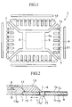
- FIG. 1 is a plan view showing a lead frame for use in a semiconductor package in accordance with a preferred embodiment of the invention;
- FIG. 2 is an enlarged cross sectional view showing essential parts of the semiconductor package, wherein a projecting portion of a lead is cut out along a cutting line A;
- FIG. 3A is an enlarged cross sectional view showing essential parts of the semiconductor package that is attached onto a circuit board;
- FIG. 3B is an enlarged plan view showing prescribed parts of the semiconductor package shown in FIG. 3A;
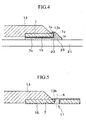
- FIG. 4 is an enlarged cross sectional view showing a modified example of the semiconductor package shown in FIGS. 3A and 3B;
- FIG. 5 is an enlarged cross sectional view showing the modified example of the semiconductor package before a cutting process;
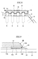
- FIG. 6 is an enlarged plan view showing a modified example of a semiconductor package in which a through hole is formed in a dam bar across a plurality of leads;
- FIG. 7 is an enlarged plan view showing the semiconductor package that is subjected to cutting so that the leads are made electrically independent of each other;
- FIG. 8 is an enlarged plan view showing a modified example of a semiconductor package in which the tip end of each lead is projected inside of an elongated through hole formed in a dam bar and is accompanied with a further projecting portion;
- FIG. 9 is an enlarged cross sectional view showing a modified example of a semiconductor package;
- FIG. 10 is an enlarged cross sectional view showing a modified example of a semiconductor package before a cutting process;
- FIG. 11 is an enlarged cross sectional view showing a modified example of a semiconductor package before a cutting process;
- FIG. 12 is an enlarged cross sectional view showing the semiconductor package shown in FIG. 11 that is attached onto a circuit board;
- FIG. 13 is a plan view showing a conventionally-known example of a lead frame for use in a semiconductor package;
- FIG. 14 is an enlarged cross sectional view showing essential parts of the semiconductor package enclosing the lead frame shown in FIG. 13 in which a projecting portion of a lead is subjected to cutting at a cutting line A; and
- FIG. 15 is an enlarged cross sectional view showing the semiconductor package attached onto a circuit board.
-
- This invention will be described in further detail by way of examples with reference to the accompanying drawings.
- The outline of a manufacturing method for a semiconductor package according to a preferred embodiment of the invention will be described with reference to FIGS. 1, 2, 3A, and 3B.
- At first, a thin metal plate made of copper and the like is subjected to one of or both of press working and etching process, thus producing a lead frame 1 (see FIG. 1) comprising a
stage 5 for mounting asemiconductor chip 3, a plurality ofleads 7 arranged in the periphery of thestage 5, and dam bars (i.e., lead interconnecting members) for interconnecting theleads 7. - In the above, a plurality of through
holes 17 penetrating through thelead frame 1 are simultaneously formed with respect to theleads 7 respectively due to the press working and/or the etching process, wherein the throughholes 17 are aligned along with the arrangements of theleads 7. - Next, the
semiconductor chip 3 is bonded onto asurface 5a of thestage 5; then, pads of thesemiconductor chip 3 are electrically connected with theleads 7 respectively viametal bonding wires 11. Herein, the bonding position of thelead 7 bonded with thebonding wire 11 is located on aprescribed surface 7a of thelead 7, which is shifted inwardly in position from the throughhole 17 towards thestage 5. - The
aforementioned lead frame 1 is arranged in a metal mold (not shown), into which a melted resin is injected so as to form a molded resin 13 (see FIG. 2) that integrally fixes thesemiconductor chip 3, thestage 5, thebonding wire 11, and the bonding portion of thelead 7 at prescribed positions. - In the above, a
backside 13a of the moldedresin 13 forms the same plane together with abackside 7b of thelead 7, wherein a prescribed side surface of the moldedresin 13 in its thickness direction lies along a cutting line A for the lead, which will be described later. That is, the prescribed side surface of the moldedresin 13 lies at a prescribed position at which the overall length of the throughhole 17, which is formed in a longitudinal direction (i.e., C-D directions) of thelead 7, is reduced to a half. The moldedresin 13 is formed to prevent a resin from being introduced into the throughhole 17. - After the formation of the molded
resin 13, asurface 7a and abackside 7b of thelead 7, which are exposed to the exterior of the moldedresin 13, and the interior wall of the throughhole 17 are subjected to plating, thus forming platedfilms 15. - Thereafter a projecting portion 7c of the
lead 7, which is projected outside of the prescribed side surface of the moldedresin 13 in the direction D, is cut out at the cutting line A together with thedam bar 9, so that theleads 7 are made electrically independent of each other, thus completing the production of the semiconductor package. - As a result, it is possible to produce a
semiconductor package 30 of a QFN type as shown in FIG. 3A, wherein thelead 7 is not projected outside of aprescribed side surface 13b of the moldedresin 13. In thesemiconductor package 30, aside surface 7d of thelead 7 in its thickness direction (see FIG. 3B) that is exposed outwardly is formed by cutting thelead 7 at the cutting line A. Specifically, theside surface 7d of thelead 7 comprises acut surface 7e, which forms the same plane as theside surface 13b of the moldedresin 13, and a concave portion (or a plated surface) 7f that forms a part of aninterior wall 17a of the throughhole 17, wherein a platedfilm 15 is formed on theconcave portion 7f. - When the
semiconductor package 30 is attached onto acircuit board 21, alower surface 13a of the moldedresin 13 is placed opposite to thecircuit board 21, wherein each of theleads 7 is electrically connected with aland portion 23 of thecircuit board 21 via asolder 25. In this state, thesolder 25 joins thebackside 7b of thelead 7 and theconcave portion 7f. - According to the aforementioned method for manufacturing the
semiconductor package 30, thelead frame 1 is formed in such a way that the throughholes 17 are formed with respect to theleads 7; then, it is subjected to plating. Hence, by cutting each of theleads 7 at the cutting line A, it is possible to easily produce thesemiconductor package 30 in which the platedfilm 15 is formed on theconcave portion 7f of theside surface 7d of thelead 7. - Due to the formation of the plated
films 15 on theconcave portion 7f of theside surface 7d forming the tip end of thelead 7 as well as thebackside 7b of thelead 7, it is possible to noticeably improve wettability, and it is possible to increase the overall adhesion area of thesolder 25 with respect to thelead 7; hence, it is possible to noticeably improve the joining strength established between thelead 7 and thesolder 25. Under the state where thesemiconductor package 30 is attached onto thecircuit board 21, the platedfilm 15 formed on theconcave portion 7f is exposed outwardly and upwardly, which makes it easy for a human inspector to perform visual inspection on the joined state between thelead 7 and thesolder 25. Therefore, it is possible to improve the reliability in establishing electrical connection between thelead 7 and theland portion 23 of thecircuit board 21 when thesemiconductor package 30 is attached onto thecircuit board 21. - The
aforementioned semiconductor package 30 is advantageous in that it is possible to reduce height dimensions measured from the surface of thecircuit board 21 when thesemiconductor package 30 is attached onto thecircuit board 21 because thebackside 7b of thelead 7 forms the same plane together with thelower surface 13a of the moldedresin 13. In short, it is possible to noticeably reduce the overall thickness of thesemiconductor package 30. - The present embodiment is designed such that the
cut surface 7e of thelead 7 is located in the same plane of theside surface 13b of the moldedresin 13. Of course, this invention is not necessarily limited to the present embodiment, which can be modified such that as shown in FIG. 4, the tip end of thelead 7 is partially projected outside of theside surface 13b of the moldedresin 13. In this case, the platedfilm 15 can remain on thesurface 7a of thelead 7 that is exposed to the exterior of the moldedresin 13. That is, when thesemiconductor package 30 is attached onto thecircuit board 21, it is possible to join thesolder 25 with thebackside 7b of thelead 7, theconcave portion 7f, and thesurface 7a; hence, it is possible to further improve the reliability in establishing electrical connection between thelead 7 and theland portion 23 of thecircuit board 21. - In the case of FIG. 4, the through
hole 17 should be formed outwardly from theside surface 13b of the moldedresin 13 as shown in FIG. 5. Alternatively, the throughhole 17 should be enlarged in dimensions in a direction as it separates off from theside surface 13b of the moldedresin 13. - The present embodiment is designed such that the
lead 7 is subjected to cutting at a prescribed cutting position at which the length of the throughhole 17 lying in the longitudinal direction of thelead 7 is reduced to a half. Of course, this invention is not necessarily limited to the present embodiment, which can be modified such that the cutting position can be set at any position of the throughhole 17. - The through
hole 17 is not necessarily formed with respect to eachlead 7. That is, the throughhole 17 can be formed at a prescribed position of thedam bar 9 interconnecting the leads 7. - That is, as shown in FIG. 6, in the formation of the lead frame, an elongated through
hole 18 is formed in an alignment direction ofleads 6 across a plurality of theleads 6, wherein theleads 6 including the interior wall of the throughhole 18 and thedam bar 9 are subjected to plating; then, thedam bar 9 is subjected to cutting at cutting lines B. Thus, it is possible to produce asemiconductor package 31 as shown in FIG. 7 in which theleads 6 are made electrically independent of each other. - In the
aforementioned semiconductor package 31, each ofside surfaces 6a of theleads 6 in their thickness directions is constituted by a platedsurface 6f forming the tip end of thelead 6 on which a platedfilm 15 is formed, and acut surface 6d that adjoins the platedsurface 6f and is positioned opposite to the otheradjacent lead 6, wherein aprescribed surface 6b adjoining theside surface 6a of thelead 6 is subjected to plating as well. - The
aforementioned semiconductor package 31 is characterized by forming a relatively large throughhole 18, which is larger than the foregoing throughhole 17 formed with respect to eachlead 7; hence, it is possible to easily increase the total area of the platedsurface 6f of thelead 6. Thus, it is possible to reliably improve the joining strength between the solder and thelead 6 by further increasing the solder adhesion area with respect to thelead 6. - When the through
hole 18 is formed in thedam bar 9, it is possible to form the tip ends of theleads 6 of thesemiconductor package 31 in advance. That is, it is possible to modify each of theleads 6 as shown in FIG. 8 such that eachlead 6 has a projectingportion 6b, which is projected inside of the throughhole 18 in the longitudinal direction (i.e., a direction E) thereof, wherein a further projectingportion 6c is formed from the projectingportion 6b of thelead 6. - Incidentally, the overall area of the plated
surface 6f is not necessarily increased by forming the further projectingportion 6c further projected inside of the throughhole 18. Instead, it is possible to form a hollow (or a recess) at the projectingportion 6b forming the tip end of thelead 6. - In the modified example of the present embodiment, the through
hole 18 is formed across a plurality ofleads 6 in the alignment direction of theleads 6, which is not restricted in this invention. That is, this invention requires that a through hole be formed at the prescribed position allowing the cutting line to pass therethrough in order to make theadjacent leads 6 electrically independent of each other. For instance, it is possible to form a through hole on the cutting line B passing between the adjacent leads 6. - In the present embodiment and its modifications, the through hole(s) is formed simultaneously with the formation of the lead frame, which is not restricted in this invention. That is, this invention requires that the through hole be formed within a time period between the formation of the lead frame and the timing to perform plating. Specifically, the through holes can be formed simultaneously with the formation of the molded
resin 13. Due to the provision of the through hole(s), it is possible to increase the overall area for the plating, and it is possible to reduce the overall cutting area for making the leads electrically independent of each other. It is therefore possible to provide an effect in which the semiconductor package can be produced with ease. - In the present embodiment and its modifications, the plated
surface 6f and theconcave portions side surface 10d of a lead 10 located in proximity to abackside 10b is subjected to plating, thus forming a plated surface 10f. When such asemiconductor package 32 shown in FIG. 9 is attached onto thecircuit board 21, thesolder 25 can join the plated surface 10f in addition to thebackside 10b of thelead 10; therefore, it is possible to improve the reliability in establishing the electrical connection between the lead 10 and theland portion 23 of thecircuit board 21. - In the above, the
semiconductor package 32 can be modified as shown in FIG. 10 such that instead of forming the foregoing throughholes hollow portion 12 should be formed by etching or machining on thebackside 10b of thelead 10 in association with the cutting line A, which is set to make the adjacent leads 10 electrically independent of each other. Herein, aninterior wall 12a of thehollow portion 12 is subjected to plating, thus forming the aforementioned plated surface 10f. - Each of the aforementioned semiconductor packages 30-32 is constituted as the QFN type, which is not restricted in this invention when the semiconductor package is not necessarily reduced in thickness. That is, each of them can be constituted as the QFP type providing the aforementioned leads 8, which are projected outside of the molded
resin 13. For example, it is possible to partially modify the aforementioned semiconductor package as shown in FIG. 11 such that the throughhole 17 is formed on a joiningportion 8a of thelead 8 joining thesolder 25, wherein theinterior wall 17a of the throughhole 17 is subjected to plating; then, thelead 8 is subjected to cutting at a cutting line A. Thus, it is possible to produce a semiconductor package as shown in FIG. 12 in which aconcave portion 8f forming aside surface 8d of the joiningportion 8a of thelead 8 joins thesolder 25, whereby it is possible to further improve the reliability in establishing the electrical connection between thelead 8 and theland portion 23 of thecircuit board 21. - As described heretofore, this invention has a variety of effects and technical features, which will be described below.
- (1) According to this invention, a lead frame is designed such that a through hole is formed with respect to a lead or a lead interconnection member (e.g., a dam bar), whereby it is possible to improve the joining strength between the lead and the solder. Herein, the lead frame mounting a semiconductor chip is enclosed in a molded resin so as to produce a semiconductor package that is attached onto a circuit board, wherein it is possible to improve the reliability with respect to the electrical connection established between the lead and the land portion of the circuit board.
- (2) When the lead frame is designed such that the through hole is elongated and is formed in the lead interconnection member, it is possible to improve the joining strength between the lead and the solder compared with the lead frame in which a relatively small through hole is formed with respect to each lead.
- (3) After formation of the through hole(s), a plating process is performed to form plated films at appropriate areas of the leads substantially enclosed in a molded resin. Herein, plating is performed on the side portions of the leads that are exposed to the exterior of the molded resin. In addition, the surfaces of the leads are formed in the same plane together with the lower surface of the molded resin, whereby it is possible to noticeably reduce the overall thickness of the semiconductor package.
-
- As this invention may be embodied in several forms without departing from the spirit or essential characteristics thereof, the present embodiment and its modified examples are therefore illustrative and not restrictive, since the scope of the invention is defined by the appended claims rather than by the description preceding them, and all changes that fall within metes and bounds of the claims, or equivalents of such metes and bounds are therefore intended to be embraced by the claims.
Claims (11)
- A lead frame comprising:wherein the plurality of lead interconnection members and the plurality of leads are subjected to cutting at the cutting lines so that the plurality of leads are made electrically independent of each other.a stage (5) for mounting a semiconductor chip (3) thereon;a plurality of groups of leads (7) arranged in a periphery of the stage;a plurality of lead interconnection members (9) for interconnecting a plurality of leads in each group of the leads respectively; anda hollow (12, 17) that is formed to concave in a thickness direction on each lead, thus allowing a plurality of cutting lines (A) to pass therethrough,
- A lead frame comprising:wherein the plurality of lead interconnection members and the plurality of leads are subjected to cutting at the cutting lines so that the plurality of leads are made electrically independent of each other.a stage (5) for mounting a semiconductor chip (3) thereon;a plurality of groups of leads (7) arranged in a periphery of the stage;a plurality of lead interconnection members (9) for interconnecting a plurality of leads in each group of the leads respectively; anda hollow (18) that is formed to concave in a thickness direction on each lead interconnection member across the plurality of leads, thus allowing a plurality of cutting lines (B) to pass therethrough,
- A manufacturing method for a semiconductor package comprising the steps of:wherein a hollow (12, 17) is formed to concave in a thickness direction of the lead frame on each lead so as to allow the plurality of cutting lines to pass therethrough, and wherein the hollow is formed at a selected timing within a time period after the lead frame is formed and before the plating is performed on the leads.forming a lead frame (1) by processing a thin metal plate, wherein the lead frame comprises a stage (5) for mounting a semiconductor chip (3) thereon, a plurality of groups of leads arranged in a periphery of the stage, and a plurality of lead interconnection members (9) for interconnecting a plurality of leads in each group of the leads respectively;mounting the semiconductor chip on the stage of the lead frame via bonding, wherein the semiconductor chip is wired with the plurality of leads;forming a molded resin (13) for integrally fixing the semiconductor chip, the stage, and the leads therein;plating prescribed surfaces of the leads that are exposed to an exterior of the molded resin; andcutting the plurality of leads at a plurality of cutting lines (A) so that the plurality of leads are made electrically independent of each other,
- A manufacturing method for a semiconductor package comprising the steps of:wherein a hollow (18) is formed to concave in a thickness direction of the lead frame on each lead interconnection member so as to allow the plurality of cutting lines to pass therethrough, and wherein the through holes are formed at a selected timing within a time period after the lead frame is formed and bcfore the plating is performed on the leads.forming a lead frame (1) by processing a thin metal plate, wherein the lcad frame comprises a stage (5) for mounting a semiconductor chip (3) thereon, a plurality of groups of leads arranged in a periphery of the stage, and a plurality of lead interconnection members (9) for interconnecting a plurality of leads in each group of the leads respectively;mounting the semiconductor chip on the stage of the lead frame via bonding, wherein the semiconductor chip is wired with the plurality of leads;forming a molded resin (13) for integrally fixing the semiconductor chip, the stage, and the leads therein;plating prescribed surfaces of the leads that are exposed to an exterior of the molded resin; andcutting the plurality of leads at a plurality of cutting lines (B) so that the plurality of leads are made electrically independent of each other,
- A semiconductor package having a plurality of leads (6, 7) that are exposed to an exterior of a molded resin (13), wherein a side surface (6a, 7d) of the lead is associated with a plated surface (6f, 7f) and a cut surface (6d, 7e) that adjoins the plated surface and that makes the adjacent leads to be electrically independent of each other.
- The semiconductor package according to claim 5, wherein a backside of the lead subjected to plating is formed in a same plane together with a lower surface (13a) of the molded resin.
- The lead frame according to claim 2, wherein each of the leads has a projecting portion (6b) that is projected inwardly into the hollow.
- The lead frame according to claim 1, wherein the hollow is replaced with a through hole (17).
- The lead frame according to claim 2, wherein the hollow is replaced with a through hole (18).
- The manufacturing method for a semiconductor package according to claim 3, wherein the hollow is formed by etching.
- The manufacturing method for a semiconductor package according to claim 4, wherein the hollow is formed by etching.
Applications Claiming Priority (2)
| Application Number | Priority Date | Filing Date | Title |
|---|---|---|---|
| JP2003099126 | 2003-04-02 | ||
| JP2003099126 | 2003-04-02 |
Publications (2)
| Publication Number | Publication Date |
|---|---|
| EP1465253A2 true EP1465253A2 (en) | 2004-10-06 |
| EP1465253A3 EP1465253A3 (en) | 2010-03-03 |
Family
ID=32844686
Family Applications (1)
| Application Number | Title | Priority Date | Filing Date |
|---|---|---|---|
| EP04007816A Withdrawn EP1465253A3 (en) | 2003-04-02 | 2004-03-31 | Semiconductor package and lead frame therefor |
Country Status (5)
| Country | Link |
|---|---|
| US (4) | US7195953B2 (en) |
| EP (1) | EP1465253A3 (en) |
| KR (2) | KR100877640B1 (en) |
| CN (2) | CN2718782Y (en) |
| TW (1) | TWI242872B (en) |
Cited By (1)
| Publication number | Priority date | Publication date | Assignee | Title |
|---|---|---|---|---|
| WO2007089209A1 (en) * | 2006-02-01 | 2007-08-09 | Infineon Technologies Ag | Fabrication of a qfn integrated circuit package |
Families Citing this family (14)
| Publication number | Priority date | Publication date | Assignee | Title |
|---|---|---|---|---|
| JP2006179760A (en) | 2004-12-24 | 2006-07-06 | Yamaha Corp | Semiconductor package and lead frame used therefor |
| US7507603B1 (en) * | 2005-12-02 | 2009-03-24 | Amkor Technology, Inc. | Etch singulated semiconductor package |
| CN101241894A (en) * | 2007-09-20 | 2008-08-13 | 三星电子株式会社 | Smart card metal carrier tape, manufacturing method thereof, and packaging module including the carrier tape |
| JP2010056372A (en) * | 2008-08-29 | 2010-03-11 | Sanyo Electric Co Ltd | Resin sealed semiconductor device, and method of manufacturing the same |
| DE102011018851B4 (en) * | 2011-04-27 | 2015-04-02 | Texas Instruments Deutschland Gmbh | Terminal block and arrangement thereof, method for producing a connectionless module |
| JP2013225595A (en) * | 2012-04-20 | 2013-10-31 | Shinko Electric Ind Co Ltd | Lead frame, semiconductor package, and manufacturing methods of lead frame and semiconductor package |
| JP5959386B2 (en) * | 2012-09-24 | 2016-08-02 | エスアイアイ・セミコンダクタ株式会社 | Resin-sealed semiconductor device and manufacturing method thereof |
| US9013030B2 (en) | 2013-03-28 | 2015-04-21 | Infineon Technologies Ag | Leadframe, semiconductor package including a leadframe and method for producing a leadframe |
| US20140299978A1 (en) * | 2013-04-03 | 2014-10-09 | Lingsen Precision Industries, Ltd. | Quad flat non-lead package |
| US8809119B1 (en) | 2013-05-17 | 2014-08-19 | Stats Chippac Ltd. | Integrated circuit packaging system with plated leads and method of manufacture thereof |
| US9048228B2 (en) | 2013-09-26 | 2015-06-02 | Stats Chippac Ltd. | Integrated circuit packaging system with side solderable leads and method of manufacture thereof |
| CN105405823A (en) * | 2014-08-20 | 2016-03-16 | 飞思卡尔半导体公司 | Semiconductor device with inspectable solder joints |
| JP2017041541A (en) * | 2015-08-20 | 2017-02-23 | 三菱電機株式会社 | High-frequency high-output device |
| JP2018056451A (en) * | 2016-09-30 | 2018-04-05 | ルネサスエレクトロニクス株式会社 | Semiconductor device |
Citations (6)
| Publication number | Priority date | Publication date | Assignee | Title |
|---|---|---|---|---|
| JPH01175758A (en) | 1987-12-29 | 1989-07-12 | Hitachi Ltd | Semiconductor device |
| US5150193A (en) | 1987-05-27 | 1992-09-22 | Hitachi, Ltd. | Resin-encapsulated semiconductor device having a particular mounting structure |
| JPH06260582A (en) * | 1993-03-09 | 1994-09-16 | Hitachi Ltd | Semiconductor device |
| EP0860877A2 (en) | 1997-02-25 | 1998-08-26 | Oki Electric Industry Co., Ltd. | Semiconductor device and method for producing thereof |
| US20030001249A1 (en) | 1999-06-30 | 2003-01-02 | Yoshihiko Shimanuki | Semiconductor device and a method of manufacturing the same and a mounting structure of a semiconductor device |
| US20030057542A1 (en) | 2001-09-21 | 2003-03-27 | Giovanni Frezza | Leads of a no-lead type package of a semiconductor device |
Family Cites Families (31)
| Publication number | Priority date | Publication date | Assignee | Title |
|---|---|---|---|---|
| US5621811A (en) * | 1987-10-30 | 1997-04-15 | Hewlett-Packard Co. | Learning method and apparatus for detecting and controlling solder defects |
| JP2708191B2 (en) * | 1988-09-20 | 1998-02-04 | 株式会社日立製作所 | Semiconductor device |
| JPH02302068A (en) | 1989-05-16 | 1990-12-14 | Nec Corp | Transfer mold type hybrid integrated circuit |
| US5117279A (en) * | 1990-03-23 | 1992-05-26 | Motorola, Inc. | Semiconductor device having a low temperature uv-cured epoxy seal |
| JPH0427148A (en) | 1990-05-22 | 1992-01-30 | Seiko Epson Corp | Lead frame for semiconductor device |
| JPH04103154A (en) | 1990-08-23 | 1992-04-06 | Fujitsu Ltd | Semiconductor device, manufacture thereof, and mounting method thereof |
| JP3008470B2 (en) | 1990-09-27 | 2000-02-14 | 大日本印刷株式会社 | Lead frame |
| JPH04171855A (en) | 1990-11-05 | 1992-06-19 | Nec Kyushu Ltd | Lead frame for semiconductor device |
| US5172214A (en) * | 1991-02-06 | 1992-12-15 | Motorola, Inc. | Leadless semiconductor device and method for making the same |
| JP2553435B2 (en) | 1992-05-11 | 1996-11-13 | 日東工器株式会社 | Function improver for fingers, etc. |
| JP3905208B2 (en) | 1997-02-27 | 2007-04-18 | 富士通株式会社 | Semiconductor device and its mounting structure |
| US5327008A (en) * | 1993-03-22 | 1994-07-05 | Motorola Inc. | Semiconductor device having universal low-stress die support and method for making the same |
| JPH06334090A (en) | 1993-05-26 | 1994-12-02 | Oki Electric Ind Co Ltd | Lead structure of resin-sealed semiconductor device and manufacturing method thereof |
| JP3152834B2 (en) * | 1993-06-24 | 2001-04-03 | 株式会社東芝 | Electronic circuit device |
| JPH0730043A (en) | 1993-07-13 | 1995-01-31 | Seiko Epson Corp | Semiconductor device and method of manufacturing semiconductor device |
| JP3243951B2 (en) | 1994-10-24 | 2002-01-07 | 株式会社村田製作所 | Electronic component manufacturing method |
| US6100598A (en) * | 1997-03-06 | 2000-08-08 | Nippon Steel Semiconductor Corporation | Sealed semiconductor device with positional deviation between upper and lower molds |
| JPH10335374A (en) * | 1997-06-04 | 1998-12-18 | Fujitsu Ltd | Semiconductor device and semiconductor device module |
| JPH118261A (en) | 1997-06-13 | 1999-01-12 | Matsushita Electric Works Ltd | Method for manufacturing semiconductor device |
| EP0895287A3 (en) * | 1997-07-31 | 2006-04-05 | Matsushita Electric Industrial Co., Ltd. | Semiconductor device and lead frame for the same |
| JPH11354705A (en) | 1998-06-04 | 1999-12-24 | Toshiba Corp | Semiconductor device and method of manufacturing semiconductor device |
| JP2001077278A (en) * | 1999-10-15 | 2001-03-23 | Amkor Technology Korea Inc | Semiconductor package, lead frame therefor, method of manufacturing semiconductor package, and mold therefor |
| US6847103B1 (en) * | 1999-11-09 | 2005-01-25 | Amkor Technology, Inc. | Semiconductor package with exposed die pad and body-locking leadframe |
| US6400004B1 (en) * | 2000-08-17 | 2002-06-04 | Advanced Semiconductor Engineering, Inc. | Leadless semiconductor package |
| JP4669166B2 (en) * | 2000-08-31 | 2011-04-13 | エルピーダメモリ株式会社 | Semiconductor device |
| US6459148B1 (en) * | 2000-11-13 | 2002-10-01 | Walsin Advanced Electronics Ltd | QFN semiconductor package |
| JP2002164497A (en) | 2000-11-29 | 2002-06-07 | Hitachi Ltd | Semiconductor device and manufacturing method thereof |
| JP4570797B2 (en) | 2001-02-14 | 2010-10-27 | ルネサスエレクトロニクス株式会社 | Manufacturing method of semiconductor device |
| JP2002359336A (en) | 2001-05-31 | 2002-12-13 | Sony Corp | Semiconductor device |
| US6608366B1 (en) * | 2002-04-15 | 2003-08-19 | Harry J. Fogelson | Lead frame with plated end leads |
| US6872599B1 (en) * | 2002-12-10 | 2005-03-29 | National Semiconductor Corporation | Enhanced solder joint strength and ease of inspection of leadless leadframe package (LLP) |
-
2004
- 2004-03-30 US US10/811,999 patent/US7195953B2/en not_active Expired - Lifetime
- 2004-03-31 KR KR1020040022052A patent/KR100877640B1/en not_active Expired - Fee Related
- 2004-03-31 EP EP04007816A patent/EP1465253A3/en not_active Withdrawn
- 2004-03-31 CN CNU2004200064626U patent/CN2718782Y/en not_active Expired - Fee Related
- 2004-03-31 TW TW093108974A patent/TWI242872B/en not_active IP Right Cessation
- 2004-03-31 CN CN200410032003XA patent/CN1534776B/en not_active Expired - Fee Related
-
2006
- 2006-06-07 US US11/447,929 patent/US20060228833A1/en not_active Abandoned
-
2007
- 2007-02-05 US US11/671,402 patent/US20070126089A1/en not_active Abandoned
- 2007-08-22 US US11/843,163 patent/US20070292994A1/en not_active Abandoned
-
2008
- 2008-10-06 KR KR1020080097832A patent/KR100947412B1/en not_active Expired - Fee Related
Patent Citations (6)
| Publication number | Priority date | Publication date | Assignee | Title |
|---|---|---|---|---|
| US5150193A (en) | 1987-05-27 | 1992-09-22 | Hitachi, Ltd. | Resin-encapsulated semiconductor device having a particular mounting structure |
| JPH01175758A (en) | 1987-12-29 | 1989-07-12 | Hitachi Ltd | Semiconductor device |
| JPH06260582A (en) * | 1993-03-09 | 1994-09-16 | Hitachi Ltd | Semiconductor device |
| EP0860877A2 (en) | 1997-02-25 | 1998-08-26 | Oki Electric Industry Co., Ltd. | Semiconductor device and method for producing thereof |
| US20030001249A1 (en) | 1999-06-30 | 2003-01-02 | Yoshihiko Shimanuki | Semiconductor device and a method of manufacturing the same and a mounting structure of a semiconductor device |
| US20030057542A1 (en) | 2001-09-21 | 2003-03-27 | Giovanni Frezza | Leads of a no-lead type package of a semiconductor device |
Cited By (3)
| Publication number | Priority date | Publication date | Assignee | Title |
|---|---|---|---|---|
| WO2007089209A1 (en) * | 2006-02-01 | 2007-08-09 | Infineon Technologies Ag | Fabrication of a qfn integrated circuit package |
| US7618845B2 (en) | 2006-02-01 | 2009-11-17 | Infineon Technologies Ag | Fabrication of an integrated circuit package |
| USRE43818E1 (en) | 2006-02-01 | 2012-11-20 | Infineon Technologies Ag | Fabrication of an integrated circuit package |
Also Published As
| Publication number | Publication date |
|---|---|
| US7195953B2 (en) | 2007-03-27 |
| CN1534776B (en) | 2010-05-26 |
| EP1465253A3 (en) | 2010-03-03 |
| KR100947412B1 (en) | 2010-03-12 |
| CN2718782Y (en) | 2005-08-17 |
| CN1534776A (en) | 2004-10-06 |
| US20040195661A1 (en) | 2004-10-07 |
| KR100877640B1 (en) | 2009-01-12 |
| US20070292994A1 (en) | 2007-12-20 |
| TW200425455A (en) | 2004-11-16 |
| US20060228833A1 (en) | 2006-10-12 |
| KR20040086205A (en) | 2004-10-08 |
| US20070126089A1 (en) | 2007-06-07 |
| TWI242872B (en) | 2005-11-01 |
| KR20080097970A (en) | 2008-11-06 |
Similar Documents
| Publication | Publication Date | Title |
|---|---|---|
| US20070292994A1 (en) | Method of manufacturing a semiconductor package using a lead frame having through holes or hollows therein | |
| US7397112B2 (en) | Semiconductor package and lead frame therefor | |
| KR100753723B1 (en) | Manufacturing Method of Semiconductor Device | |
| KR101131353B1 (en) | Semiconductor device | |
| US20030209815A1 (en) | Semiconductor device and its manufacturing method | |
| KR200492009Y1 (en) | Preformed lead frame and lead frame package made from the same | |
| US6608369B2 (en) | Lead frame, semiconductor device and manufacturing method thereof, circuit board and electronic equipment | |
| US20010007782A1 (en) | Integrated circuit chip and method for fabricating the same | |
| JP3915794B2 (en) | Semiconductor package, manufacturing method thereof, and lead frame used for the same | |
| JP4600124B2 (en) | Manufacturing method of semiconductor package | |
| US11728179B2 (en) | Surface mount semiconductor device and method of manufacture | |
| KR100608349B1 (en) | BA Stack Package using Uneven Stacked Substrate and Manufacturing Method Thereof | |
| KR100206941B1 (en) | Trunk Lead Package and Manufacturing Method | |
| JP6294540B1 (en) | Manufacturing method and structure of lead frame with wiring | |
| KR100209763B1 (en) | Method for manufacturing of semiconductor package | |
| KR19980035063A (en) | Structure of the board on which the package is mounted | |
| JPH06209065A (en) | Electronic component mounting device | |
| KR0123425B1 (en) | Semiconductor package and the mounting method having cut outer lead | |
| HK1066098A (en) | Semiconductor package and lead frame therefor | |
| CN119108368A (en) | Packaged semiconductor device and manufacturing method | |
| JP2001177039A (en) | Semiconductor device and method of manufacturing the same | |
| KR19980052647A (en) | Lead Frame for Semiconductor Chip Package | |
| JPH06209070A (en) | Method for manufacturing semiconductor device | |
| JPH0969599A (en) | Resin-sealed semiconductor device | |
| KR19980044548A (en) | Electrical connection structure |
Legal Events
| Date | Code | Title | Description |
|---|---|---|---|
| PUAI | Public reference made under article 153(3) epc to a published international application that has entered the european phase |
Free format text: ORIGINAL CODE: 0009012 |
|
| AK | Designated contracting states |
Kind code of ref document: A2 Designated state(s): AT BE BG CH CY CZ DE DK EE ES FI FR GB GR HU IE IT LI LU MC NL PL PT RO SE SI SK TR |
|
| AX | Request for extension of the european patent |
Extension state: AL LT LV MK |
|
| RAP1 | Party data changed (applicant data changed or rights of an application transferred) |
Owner name: YAMAHA CORPORATION |
|
| RIC1 | Information provided on ipc code assigned before grant |
Ipc: H01L 23/31 20060101ALI20091021BHEP Ipc: H01L 23/495 20060101AFI20040720BHEP |
|
| PUAL | Search report despatched |
Free format text: ORIGINAL CODE: 0009013 |
|
| AK | Designated contracting states |
Kind code of ref document: A3 Designated state(s): AT BE BG CH CY CZ DE DK EE ES FI FR GB GR HU IE IT LI LU MC NL PL PT RO SE SI SK TR |
|
| AX | Request for extension of the european patent |
Extension state: AL LT LV MK |
|
| 17P | Request for examination filed |
Effective date: 20100325 |
|
| 17Q | First examination report despatched |
Effective date: 20100430 |
|
| AKX | Designation fees paid |
Designated state(s): DE FR GB |
|
| STAA | Information on the status of an ep patent application or granted ep patent |
Free format text: STATUS: THE APPLICATION IS DEEMED TO BE WITHDRAWN |
|
| 18D | Application deemed to be withdrawn |
Effective date: 20120321 |