EP1463128A2 - Method of producing photovoltaic device - Google Patents
Method of producing photovoltaic device Download PDFInfo
- Publication number
- EP1463128A2 EP1463128A2 EP04007128A EP04007128A EP1463128A2 EP 1463128 A2 EP1463128 A2 EP 1463128A2 EP 04007128 A EP04007128 A EP 04007128A EP 04007128 A EP04007128 A EP 04007128A EP 1463128 A2 EP1463128 A2 EP 1463128A2
- Authority
- EP
- European Patent Office
- Prior art keywords
- zinc oxide
- oxide layer
- layer
- substrate
- chamber
- Prior art date
- Legal status (The legal status is an assumption and is not a legal conclusion. Google has not performed a legal analysis and makes no representation as to the accuracy of the status listed.)
- Withdrawn
Links
- 238000000034 method Methods 0.000 title claims abstract description 35
- XLOMVQKBTHCTTD-UHFFFAOYSA-N Zinc monoxide Chemical compound [Zn]=O XLOMVQKBTHCTTD-UHFFFAOYSA-N 0.000 claims abstract description 310
- 239000011787 zinc oxide Substances 0.000 claims abstract description 155
- 239000000758 substrate Substances 0.000 claims abstract description 119
- 230000008021 deposition Effects 0.000 claims abstract description 85
- 239000007789 gas Substances 0.000 claims abstract description 74
- 239000004065 semiconductor Substances 0.000 claims abstract description 66
- 238000009832 plasma treatment Methods 0.000 claims abstract description 41
- IJGRMHOSHXDMSA-UHFFFAOYSA-N Atomic nitrogen Chemical compound N#N IJGRMHOSHXDMSA-UHFFFAOYSA-N 0.000 claims abstract description 17
- 229910001873 dinitrogen Inorganic materials 0.000 claims abstract description 15
- 229910052739 hydrogen Inorganic materials 0.000 claims abstract description 11
- UFHFLCQGNIYNRP-UHFFFAOYSA-N Hydrogen Chemical compound [H][H] UFHFLCQGNIYNRP-UHFFFAOYSA-N 0.000 claims abstract description 7
- 239000001257 hydrogen Substances 0.000 claims abstract description 7
- 239000002210 silicon-based material Substances 0.000 claims abstract description 6
- 229910021421 monocrystalline silicon Inorganic materials 0.000 claims abstract description 5
- 238000000151 deposition Methods 0.000 claims description 98
- 238000004544 sputter deposition Methods 0.000 claims description 25
- 230000003449 preventive effect Effects 0.000 claims description 11
- 238000001179 sorption measurement Methods 0.000 claims description 11
- 229910052734 helium Inorganic materials 0.000 claims description 5
- 229910052786 argon Inorganic materials 0.000 claims description 4
- 229910052743 krypton Inorganic materials 0.000 claims description 3
- 229910052754 neon Inorganic materials 0.000 claims description 3
- 239000010410 layer Substances 0.000 description 230
- 239000010408 film Substances 0.000 description 60
- 230000000052 comparative effect Effects 0.000 description 34
- XLYOFNOQVPJJNP-UHFFFAOYSA-N water Substances O XLYOFNOQVPJJNP-UHFFFAOYSA-N 0.000 description 33
- 239000007864 aqueous solution Substances 0.000 description 16
- 238000006243 chemical reaction Methods 0.000 description 16
- 238000001035 drying Methods 0.000 description 16
- 239000000463 material Substances 0.000 description 16
- 229910052751 metal Inorganic materials 0.000 description 16
- 239000002184 metal Substances 0.000 description 16
- 230000006866 deterioration Effects 0.000 description 15
- 239000010409 thin film Substances 0.000 description 11
- 230000000694 effects Effects 0.000 description 9
- 230000003287 optical effect Effects 0.000 description 9
- 230000008569 process Effects 0.000 description 9
- 238000012360 testing method Methods 0.000 description 9
- 230000001276 controlling effect Effects 0.000 description 8
- 238000010438 heat treatment Methods 0.000 description 7
- 238000004519 manufacturing process Methods 0.000 description 7
- -1 nitric acid ion Chemical class 0.000 description 7
- 238000005268 plasma chemical vapour deposition Methods 0.000 description 7
- 239000010935 stainless steel Substances 0.000 description 7
- 229910001220 stainless steel Inorganic materials 0.000 description 7
- 229910021424 microcrystalline silicon Inorganic materials 0.000 description 6
- 229910052709 silver Inorganic materials 0.000 description 6
- 239000011701 zinc Substances 0.000 description 6
- HCHKCACWOHOZIP-UHFFFAOYSA-N Zinc Chemical compound [Zn] HCHKCACWOHOZIP-UHFFFAOYSA-N 0.000 description 5
- PTFCDOFLOPIGGS-UHFFFAOYSA-N Zinc dication Chemical compound [Zn+2] PTFCDOFLOPIGGS-UHFFFAOYSA-N 0.000 description 5
- 229910021417 amorphous silicon Inorganic materials 0.000 description 5
- 230000015572 biosynthetic process Effects 0.000 description 5
- 239000013078 crystal Substances 0.000 description 5
- 230000001965 increasing effect Effects 0.000 description 5
- 150000002500 ions Chemical class 0.000 description 5
- 229910017604 nitric acid Inorganic materials 0.000 description 5
- 230000002829 reductive effect Effects 0.000 description 5
- 229910052725 zinc Inorganic materials 0.000 description 5
- BQCADISMDOOEFD-UHFFFAOYSA-N Silver Chemical compound [Ag] BQCADISMDOOEFD-UHFFFAOYSA-N 0.000 description 4
- CZMRCDWAGMRECN-UGDNZRGBSA-N Sucrose Chemical compound O[C@H]1[C@H](O)[C@@H](CO)O[C@@]1(CO)O[C@@H]1[C@H](O)[C@@H](O)[C@H](O)[C@@H](CO)O1 CZMRCDWAGMRECN-UGDNZRGBSA-N 0.000 description 4
- 229930006000 Sucrose Natural products 0.000 description 4
- 125000004429 atom Chemical group 0.000 description 4
- QVGXLLKOCUKJST-UHFFFAOYSA-N atomic oxygen Chemical compound [O] QVGXLLKOCUKJST-UHFFFAOYSA-N 0.000 description 4
- 235000013681 dietary sucrose Nutrition 0.000 description 4
- 238000010790 dilution Methods 0.000 description 4
- 239000012895 dilution Substances 0.000 description 4
- 239000008151 electrolyte solution Substances 0.000 description 4
- 239000001301 oxygen Substances 0.000 description 4
- 229910052760 oxygen Inorganic materials 0.000 description 4
- 239000004332 silver Substances 0.000 description 4
- 229960004793 sucrose Drugs 0.000 description 4
- 238000002834 transmittance Methods 0.000 description 4
- 229920001353 Dextrin Polymers 0.000 description 3
- 239000004375 Dextrin Substances 0.000 description 3
- BLRPTPMANUNPDV-UHFFFAOYSA-N Silane Chemical compound [SiH4] BLRPTPMANUNPDV-UHFFFAOYSA-N 0.000 description 3
- XUIMIQQOPSSXEZ-UHFFFAOYSA-N Silicon Chemical compound [Si] XUIMIQQOPSSXEZ-UHFFFAOYSA-N 0.000 description 3
- 238000011109 contamination Methods 0.000 description 3
- 235000019425 dextrin Nutrition 0.000 description 3
- 230000007613 environmental effect Effects 0.000 description 3
- 238000001704 evaporation Methods 0.000 description 3
- 229910052737 gold Inorganic materials 0.000 description 3
- 239000010931 gold Substances 0.000 description 3
- 230000006872 improvement Effects 0.000 description 3
- PJXISJQVUVHSOJ-UHFFFAOYSA-N indium(III) oxide Inorganic materials [O-2].[O-2].[O-2].[In+3].[In+3] PJXISJQVUVHSOJ-UHFFFAOYSA-N 0.000 description 3
- 238000005259 measurement Methods 0.000 description 3
- 239000000203 mixture Substances 0.000 description 3
- 238000010248 power generation Methods 0.000 description 3
- 238000012545 processing Methods 0.000 description 3
- 229910052710 silicon Inorganic materials 0.000 description 3
- 239000010703 silicon Substances 0.000 description 3
- 239000000243 solution Substances 0.000 description 3
- 238000001228 spectrum Methods 0.000 description 3
- XOLBLPGZBRYERU-UHFFFAOYSA-N tin dioxide Chemical compound O=[Sn]=O XOLBLPGZBRYERU-UHFFFAOYSA-N 0.000 description 3
- XKRFYHLGVUSROY-UHFFFAOYSA-N Argon Chemical compound [Ar] XKRFYHLGVUSROY-UHFFFAOYSA-N 0.000 description 2
- MYMOFIZGZYHOMD-UHFFFAOYSA-N Dioxygen Chemical compound O=O MYMOFIZGZYHOMD-UHFFFAOYSA-N 0.000 description 2
- 229910000577 Silicon-germanium Inorganic materials 0.000 description 2
- OLBVUFHMDRJKTK-UHFFFAOYSA-N [N].[O] Chemical compound [N].[O] OLBVUFHMDRJKTK-UHFFFAOYSA-N 0.000 description 2
- 229910045601 alloy Inorganic materials 0.000 description 2
- 239000000956 alloy Substances 0.000 description 2
- 239000012300 argon atmosphere Substances 0.000 description 2
- 239000012298 atmosphere Substances 0.000 description 2
- 210000000988 bone and bone Anatomy 0.000 description 2
- 238000004140 cleaning Methods 0.000 description 2
- 150000001875 compounds Chemical class 0.000 description 2
- 239000000470 constituent Substances 0.000 description 2
- 238000010276 construction Methods 0.000 description 2
- 229910052802 copper Inorganic materials 0.000 description 2
- 239000010949 copper Substances 0.000 description 2
- 230000007423 decrease Effects 0.000 description 2
- 230000003247 decreasing effect Effects 0.000 description 2
- 229910001882 dioxygen Inorganic materials 0.000 description 2
- 230000008020 evaporation Effects 0.000 description 2
- 239000001307 helium Substances 0.000 description 2
- SWQJXJOGLNCZEY-UHFFFAOYSA-N helium atom Chemical compound [He] SWQJXJOGLNCZEY-UHFFFAOYSA-N 0.000 description 2
- 239000012535 impurity Substances 0.000 description 2
- 230000001678 irradiating effect Effects 0.000 description 2
- 230000007246 mechanism Effects 0.000 description 2
- 150000002739 metals Chemical class 0.000 description 2
- 238000002156 mixing Methods 0.000 description 2
- 230000036961 partial effect Effects 0.000 description 2
- 230000001681 protective effect Effects 0.000 description 2
- 230000001105 regulatory effect Effects 0.000 description 2
- 238000007738 vacuum evaporation Methods 0.000 description 2
- 238000004804 winding Methods 0.000 description 2
- 229910052724 xenon Inorganic materials 0.000 description 2
- ONDPHDOFVYQSGI-UHFFFAOYSA-N zinc nitrate Chemical compound [Zn+2].[O-][N+]([O-])=O.[O-][N+]([O-])=O ONDPHDOFVYQSGI-UHFFFAOYSA-N 0.000 description 2
- RYGMFSIKBFXOCR-UHFFFAOYSA-N Copper Chemical compound [Cu] RYGMFSIKBFXOCR-UHFFFAOYSA-N 0.000 description 1
- 208000005156 Dehydration Diseases 0.000 description 1
- 239000004642 Polyimide Substances 0.000 description 1
- 229910004014 SiF4 Inorganic materials 0.000 description 1
- 229910000831 Steel Inorganic materials 0.000 description 1
- 238000010521 absorption reaction Methods 0.000 description 1
- 230000002411 adverse Effects 0.000 description 1
- 229910052782 aluminium Inorganic materials 0.000 description 1
- XAGFODPZIPBFFR-UHFFFAOYSA-N aluminium Chemical compound [Al] XAGFODPZIPBFFR-UHFFFAOYSA-N 0.000 description 1
- 230000002547 anomalous effect Effects 0.000 description 1
- 239000004760 aramid Substances 0.000 description 1
- 229920003235 aromatic polyamide Polymers 0.000 description 1
- 229910001423 beryllium ion Inorganic materials 0.000 description 1
- 150000001720 carbohydrates Chemical class 0.000 description 1
- 235000014633 carbohydrates Nutrition 0.000 description 1
- 229910052799 carbon Inorganic materials 0.000 description 1
- 239000000919 ceramic Substances 0.000 description 1
- 229910052804 chromium Inorganic materials 0.000 description 1
- 239000011248 coating agent Substances 0.000 description 1
- 238000000576 coating method Methods 0.000 description 1
- 239000004020 conductor Substances 0.000 description 1
- 230000010485 coping Effects 0.000 description 1
- 230000007797 corrosion Effects 0.000 description 1
- 238000005260 corrosion Methods 0.000 description 1
- 230000007547 defect Effects 0.000 description 1
- 230000018044 dehydration Effects 0.000 description 1
- 238000006297 dehydration reaction Methods 0.000 description 1
- 238000011161 development Methods 0.000 description 1
- 230000018109 developmental process Effects 0.000 description 1
- 239000002019 doping agent Substances 0.000 description 1
- 230000005611 electricity Effects 0.000 description 1
- 238000003912 environmental pollution Methods 0.000 description 1
- 229910052732 germanium Inorganic materials 0.000 description 1
- 239000011521 glass Substances 0.000 description 1
- PCHJSUWPFVWCPO-UHFFFAOYSA-N gold Chemical compound [Au] PCHJSUWPFVWCPO-UHFFFAOYSA-N 0.000 description 1
- 125000005843 halogen group Chemical group 0.000 description 1
- 150000002431 hydrogen Chemical class 0.000 description 1
- 238000007654 immersion Methods 0.000 description 1
- 229910003437 indium oxide Inorganic materials 0.000 description 1
- MRNHPUHPBOKKQT-UHFFFAOYSA-N indium;tin;hydrate Chemical compound O.[In].[Sn] MRNHPUHPBOKKQT-UHFFFAOYSA-N 0.000 description 1
- 230000001939 inductive effect Effects 0.000 description 1
- 239000011261 inert gas Substances 0.000 description 1
- 238000002347 injection Methods 0.000 description 1
- 239000007924 injection Substances 0.000 description 1
- 238000011835 investigation Methods 0.000 description 1
- 238000011068 loading method Methods 0.000 description 1
- 238000001755 magnetron sputter deposition Methods 0.000 description 1
- 238000012544 monitoring process Methods 0.000 description 1
- 229910052757 nitrogen Inorganic materials 0.000 description 1
- 239000004745 nonwoven fabric Substances 0.000 description 1
- 229920001721 polyimide Polymers 0.000 description 1
- 238000007639 printing Methods 0.000 description 1
- 239000011241 protective layer Substances 0.000 description 1
- 238000010926 purge Methods 0.000 description 1
- 230000005855 radiation Effects 0.000 description 1
- 230000009257 reactivity Effects 0.000 description 1
- 230000002787 reinforcement Effects 0.000 description 1
- 238000011160 research Methods 0.000 description 1
- 239000011347 resin Substances 0.000 description 1
- 229920005989 resin Polymers 0.000 description 1
- 230000002441 reversible effect Effects 0.000 description 1
- ABTOQLMXBSRXSM-UHFFFAOYSA-N silicon tetrafluoride Chemical compound F[Si](F)(F)F ABTOQLMXBSRXSM-UHFFFAOYSA-N 0.000 description 1
- 150000003378 silver Chemical group 0.000 description 1
- 239000010944 silver (metal) Substances 0.000 description 1
- 229910000679 solder Inorganic materials 0.000 description 1
- 239000007921 spray Substances 0.000 description 1
- 239000010959 steel Substances 0.000 description 1
- 238000003756 stirring Methods 0.000 description 1
- 239000000126 substance Substances 0.000 description 1
- 229910001887 tin oxide Inorganic materials 0.000 description 1
- 230000000007 visual effect Effects 0.000 description 1
- 238000010792 warming Methods 0.000 description 1
Images
Classifications
-
- H—ELECTRICITY
- H10—SEMICONDUCTOR DEVICES; ELECTRIC SOLID-STATE DEVICES NOT OTHERWISE PROVIDED FOR
- H10F—INORGANIC SEMICONDUCTOR DEVICES SENSITIVE TO INFRARED RADIATION, LIGHT, ELECTROMAGNETIC RADIATION OF SHORTER WAVELENGTH OR CORPUSCULAR RADIATION
- H10F71/00—Manufacture or treatment of devices covered by this subclass
-
- C—CHEMISTRY; METALLURGY
- C25—ELECTROLYTIC OR ELECTROPHORETIC PROCESSES; APPARATUS THEREFOR
- C25D—PROCESSES FOR THE ELECTROLYTIC OR ELECTROPHORETIC PRODUCTION OF COATINGS; ELECTROFORMING; APPARATUS THEREFOR
- C25D9/00—Electrolytic coating other than with metals
- C25D9/04—Electrolytic coating other than with metals with inorganic materials
-
- H—ELECTRICITY
- H10—SEMICONDUCTOR DEVICES; ELECTRIC SOLID-STATE DEVICES NOT OTHERWISE PROVIDED FOR
- H10F—INORGANIC SEMICONDUCTOR DEVICES SENSITIVE TO INFRARED RADIATION, LIGHT, ELECTROMAGNETIC RADIATION OF SHORTER WAVELENGTH OR CORPUSCULAR RADIATION
- H10F77/00—Constructional details of devices covered by this subclass
- H10F77/40—Optical elements or arrangements
- H10F77/42—Optical elements or arrangements directly associated or integrated with photovoltaic cells, e.g. light-reflecting means or light-concentrating means
- H10F77/48—Back surface reflectors [BSR]
-
- Y—GENERAL TAGGING OF NEW TECHNOLOGICAL DEVELOPMENTS; GENERAL TAGGING OF CROSS-SECTIONAL TECHNOLOGIES SPANNING OVER SEVERAL SECTIONS OF THE IPC; TECHNICAL SUBJECTS COVERED BY FORMER USPC CROSS-REFERENCE ART COLLECTIONS [XRACs] AND DIGESTS
- Y02—TECHNOLOGIES OR APPLICATIONS FOR MITIGATION OR ADAPTATION AGAINST CLIMATE CHANGE
- Y02E—REDUCTION OF GREENHOUSE GAS [GHG] EMISSIONS, RELATED TO ENERGY GENERATION, TRANSMISSION OR DISTRIBUTION
- Y02E10/00—Energy generation through renewable energy sources
- Y02E10/50—Photovoltaic [PV] energy
- Y02E10/52—PV systems with concentrators
Definitions
- the electrically conductive substrate 203 is used the above-described substrate 101 with a metal layer 102 formed thereon.
- the counter electrode 204 of the apparatus is a buffed zinc plate and used as an anode.
- the zinc content in the zinc plate is preferably 90% or more and more preferably 99% or more.
- microwave (MW) plasma CVD or high frequency (RF, VHF) CVD is suitably used.
- the counter electrode 307 includes one or more square zinc plates of 99.99% purity.
- the DC power source 308 is controlled so that a voltage is applied across the substrate in a continuous length 303, as a cathode, and the counter electrode 307, as an anode, to keep current flow constant.
- the substrate strip 508 is, for example, a conductive substrate strip of stainless steel sheet 0.13 mm thick and 36 cm wide. While the substrate strip is being wound off from the feeding chamber 505, continuously conveyed to pass through 4 deposition chambers 504, 501, 502 and 503 and wound up into the wind-up chamber 506, an adsorption preventive layer and a three-layered nip (or pin) structure silicon non-single crystal semiconductor film for a photovoltaic device are formed on the surface of the substrate strip.
- the plasma treatment with a rare gas or nitrogen gas is carried out by plasma CVD, just as is done the semiconductor deposition; therefore, the treatment chamber is easy to place in the front portion of the semiconductor deposition apparatus.
- the treatment temperature is preferably the same as the temperature at which the doped layer adjacent to the zinc oxide layer is deposited and the treatment pressure is preferably 10 to 2,500 Pa.
- the making power is suitably in the range of 0.1 to 2.0 W, though it varies depending on the frequency of the high-frequency power source, the distance between the substrate and the cathode and the pressure in the chamber.
- a zinc oxide film was formed on a substrate in the same manner as in Example 1, and then the substrate 602 was introduced into a heat treatment chamber 601 shown in FIG. 6 and dehydrated for 10 minutes while increasing the temperature of the object to be treated (substrate) from room temperature up to 200°C in increments of 2.0°C/min and, after completing the temperature increase, controlling the same with a heater output system 606 so as to keep the object to be treated at 200°C.
- a heater output system 606 so as to keep the object to be treated at 200°C.
- each substrate was set in the substrate holder 425 and set on the rail 424 of the load chamber 401. Then the load chamber 401 was evacuated to a vacuum degree of several hundreds Pa or less.
Landscapes
- Chemical & Material Sciences (AREA)
- Inorganic Chemistry (AREA)
- Engineering & Computer Science (AREA)
- Chemical Kinetics & Catalysis (AREA)
- Electrochemistry (AREA)
- Materials Engineering (AREA)
- Metallurgy (AREA)
- Organic Chemistry (AREA)
- Photovoltaic Devices (AREA)
Abstract
There is disclosed a method of producing a
photovoltaic device, characterized in that it
includes steps of: a step of forming a zinc oxide
layer on a substrate at least by electrolytic
deposition; subjecting the zinc oxide layer to any
one treatment selected from the group consisting of
plasma treatment with a rare gas or nitrogen gas, ion
irradiation, light irradiation and electromagnetic
irradiation; and forming on the zinc oxide layer a
semiconductor layer that are made up of a non-single
crystal silicon material containing hydrogen and have
at least one p-i-n junction.
Description
The present invention relates to a method of
producing a photovoltaic device. The invention is
applicable to methods of producing, for example, a
photovoltaic device made up of a silicon non-single
crystal semiconductor material or a photovoltaic
device such as optical sensor.
In recent years, as worldwide power demand has
rapidly increased and power production has been
actively pursued to meet such demand, serious
problems have arisen with environmental pollution.
Under these conditions, electric power generation
methods using a photovoltaic device, which utilizes
the sun's rays, have lately attracted considerable
attention as clean electric power generation methods
which are probably capable of coping with future
increase in power demands while avoiding
environmental disruption, because they do not cause
problems with, for example, contamination by
radiation and global warming by the release of
greenhouse effect gases, their energy sources are
less maldistributed because the sun's rays pour all
parts of the earth, and because they provides
relatively high electricity generation efficiency
while requiring no complicated and large-scale
facility. And various investigations and developments
of such methods have been made aiming at the
practical use thereof.
To establish an electric power generation method
which uses a photovoltaic device as a method capable
of meeting the power demand described above, the
photovoltaic device is required basically to have
sufficiently high photoelectric conversion efficiency,
excel in characteristic stability and be able to be
mass-produced at low cost.
To enhance the light collecting efficiency at
long wavelengths, a back-side reflecting layer is
used in a photovoltaic device. As such a reflecting
layer, is preferable a layer which exhibits effective
reflecting characteristics at wavelengths near the
band edge of semiconductor materials and where its
absorption decreases, specifically at wavelengths of
800 nm to 1,200 nm. Layers that meet the above
requirements include, for example, layers of metals,
such as gold, silver, copper and aluminum, and the
alloys thereof. Further, attempts have been made to
improve short-circuit current density Jsc by making
effective use of reflecting light while providing an
uneven transparent conductive layer, which is
optically transparent in the specified wavelength
range, known as optical confinement. The transparent
conductive layer also serves to prevent the
deterioration in characteristics caused by a shunt
path. Very generally, these layers are formed by
vacuum evaporation or sputtering and contribute to
the improvement in short-circuit current density.
For example, the reflectance and texture
structure of reflecting layers made up of silver atom
are examined in "Optical Confinement Effect in a-SiGe
Solar Battery on 29p-MF-22 Stainless Substrate,"
(collected papers for 51st Academic Lecture by the
Applied Physics Society of Japan, Fall, 1990): p747
and in Sannomiya et al., "P-IA-15a-SiC/a-Si/a-Sie
Multi-Bandgap Stacked Solor Cells With Bandgap
Profiling," Technical Digest of the International
PVSEC-5 Kyoto, Japan, 1990: p381. These examples
state that increase in short-circuit current has been
accomplished in such a manner as to provide an
effective unevenness by forming a reflecting layer as
a two-layer deposit of silver while changing the
substrate temperature and produce optical confinement
effect by combining the uneven layer with a zinc
oxide layer.
Japanese Patent No. 3273294 discloses that a
zinc oxide layer formed using a zinc-oxide-layer
forming electrolyte solution which is made up of an
aqueous solution containing 0.001 mol/l to 0.5 mol/l
of zinc ion and 0.001 mol/l to 0.5 mol/l of nitric
acid ion is uniform in thickness and composition and
excel in optical transparency.
Japanese Patent Application Laid-Open No. H10-140373
discloses that with a method of forming a zinc
oxide thin film, characterized in that it includes: a
step of forming a first zinc oxide thin film on a
substrate by sputtering; and a step of forming a
second zinc oxide thin film on the above first zinc
oxide thin film in such a manner as to immerse the
above substrate in an aqueous solution that contains
at least nitric acid ion, zinc ion and carbohydrate
and apply current across the substrate and an
electrode having been immersed in the same solution,
a zinc oxide thin film can be formed less costly, a
zinc oxide thin film can be prevented from
anomalously growing, and a zinc oxide thin film
having excellent adhesion to a substrate can be
formed.
Japanese Patent Application Laid-Open No. 2001-152390
discloses that a zinc oxide layer formed using
a zinc-oxide-layer forming electrolyte solution which
is made up of an aqueous solution shows a high
electric resistance due to the water adsorbed
thereon; however, the electric resistance can be
decreased by heat drying the zinc oxide layer.
Further, Japanese Patent Application Laid-Open No.
2002-237606 discloses that a solar cell produced in
such a manner as to decrease the water content in a
zinc oxide layer to 7.5 × 10⁻³ mol/cm3 and form a
semiconductor layer on the zinc oxide layer has
improved photoelectric conversion efficiency.
Japanese Patent Application Laid-Open No. 2001-339079
discloses a method of producing a photovoltaic
device, characterized in that it includes: a step of
treating the surface of a transparent conductive film
of zinc oxide etc., with rare gas plasma; and a step
of forming an amorphous semiconductor layer of one
conductive type by deposition thereof on the surface
area of the transparent conductive film having been
treated with rare gas plasma. The specification
states that the treating with rare gas plasma allows
the formation of a low crystalline area on the
surface of the transparent conductive film, which
results in improvement in ohmic characteristics in
the interface of the transparent conductive film and
the semiconductor layer.
As described above, the use of a zinc oxide film
electrochemically deposited from an aqueous solution
as a reflecting layer of a solar cell permits the
solar cell to be high in photoelectric conversion
efficiency to some extent and less costly.
In the present state, however, several problems
remain to be solved to realize a solar cell of high
photoelectric conversion efficiency and less cost. To
obtain a solar cell of higher conversion efficiency,
for example, the electric resistance value of its
zinc oxide layer has to be controlled in the optimum
range, and at the same time, the transmittance of
light also has to be controlled in the optimum range.
Thus, dehydrating treatment is indispensable to
the zinc oxide layer prepared from an aqueous
solution. However, in heat drying as means of
dehydrating treatment, its temperature control is
very difficult. With temperatures so high as to
dispel all the water in the zinc oxide layer, the
reflectance of the layer is lowered, whereas with
insufficient heat drying, the water dispelled due to
the temperature increase at the time of subsequent
semiconductor layer and transparent electrode forming
operations might become a source of contamination of
the semiconductor layer and the transparent electrode.
Besides, the inventors of this invention found,
during the course of this invention, that when
forming a semiconductor layer on an insufficiently
heat dried substrate, peeling could sometimes occur
in the interface of the zinc oxide layer and the
semiconductor film. This peeling might cause a shunt,
and a problem arises with the reliability of the
device in practical use.
Further, when a zinc oxide film is formed over a
large area, due to the nonuniformity of its thickness
or the variation in the crystal form, the film is not
always dried uniformly even under the same drying
conditions. Thus, when dry treating a great deal of
zinc oxide films, the above described problems, due
to the insufficient drying or overdrying of the film,
remain to be solved.
In the light of the above-described problems,
the object of this invention is to dispel water in a
zinc oxide layer formed from an aqueous solution
while avoiding the deterioration in reflectance of
the layer and provide a photovoltaic device on the
zinc oxide layer which excels in adhesion to the
layer, and hence frees from peeling.
Thus, this invention is a method of producing a
photovoltaic device, characterized in that it
includes: a step of forming a zinc oxide layer on a
substrate at least by electrolytic deposition; a step
of giving the zinc oxide layer any one treatment
selected from the group consisting of plasma
treatment with a rare gas or nitrogen gas, ion
irradiation treatment, light irradiation treatment
and electromagnetic irradiation treatment; and a step
of forming on the zinc oxide layer a semiconductor
layer that are made up of a non-single crystal
silicon material containing hydrogen and have at
least one p-i-n junction.
In this invention, it is preferable to give the
zinc oxide layer rare gas plasma treatment, as the
above treatment, using at least one rare gas selected
from the group consisting of He, Ne, Ar, Kr and Xe.
It is also preferable to form another zinc oxide
layer by sputtering before forming the above zinc
oxide layer and use the same as an underlying layer.
Preferably the average thickness of the zinc
oxide layer is 10 nm or more and 5 µm or less.
Preferably the zinc oxide layer transmits 50% or
more of light with wavelength of 800 nm.
Preferably the zinc oxide layer has a
resistivity lower than that of the p- or n-type
semiconductor layer provided adjacent to the zinc
oxide layer.
Preferably an adsorption preventive layer is
provided between the zinc oxide layer and the p- or
n-type semiconductor layer provided adjacent to the
above zinc oxide layer.
According to this invention, water content in a
zinc oxide layer which is formed from an aqueous
solution can be reduced, while avoiding the
deterioration in transmittance of the layer, by
giving the layer plasma treatment with a rare gas or
nitrogen gas, and besides, a semiconductor layer
deposited on the zinc oxide layer is allowed to have
high photoelectric conversion efficiency and be free
from peeling, thereby a photovoltaic device that
offers high efficiency and durability under various
environmental conditions is realized.
The inventors of this invention tried to reduce
water content in a zinc oxide layer, which was formed
on a substrate using a zinc oxide layer forming
electrolyte solution made up of an aqueous solution,
while avoiding the deterioration in transmittance of
the same layer, and besides, increase the
photoelectric conversion efficiency of a
semiconductor layer deposited on the zinc oxide layer
and prevent the peeling of the same by giving the
zinc oxide layer plasma treatment with a rare gas or
nitrogen gas.
In the following the advantages will be
described which the preferred embodiments of this
invention offer.
After directing tremendous research effort
toward the solution of the above described problems,
the inventors have found that a photovoltaic device
offering high photoelectric conversion efficiency and
durability under various environmental conditions can
be produced in such a manner as to form a zinc oxide
layer on a substrate by electrolytic deposition, give
the zinc oxide layer surface plasma treatment using a
rare gas or nitrogen gas, and form on the plasma
treated zinc oxide layer semiconductor layers that
are made up of non-single crystal silicon material
containing hydrogen and have p-i-n junction. The
treatment given the zinc oxide layer surface may be
other than plasma treatment, for example, it may be
ion irradiation treatment, light irradiation
treatment or electromagnetic irradiation treatment.
Preferably the treatment of this invention is carried
out while avoiding the deterioration in crystallinity
of the zinc oxide layer surface.
The circumstances and details of this invention
will be described below in terms of treatment of the
zinc oxide layer of this invention.
As described above, when a zinc oxide layer is
formed using a zinc oxide layer forming electrolytic
solution made up of an aqueous solution, water
contamination of the layer is unavoidable; therefore,
a step is required of removing water in the layer by
heat drying after the layer formation. However,
excessive heat drying causes deterioration in
reflectance of the layer. This is probably because
excessive heat drying dispels oxygen in the zinc
oxide layer at the same time that it dispels water in
the same and the layer becomes rich Zn. There is
proposed a method in which heat drying is performed
while controlling the temperature of the layer so as
to prevent the deterioration in reflectance of the
layer; however, it is very difficult to control the
temperature of the layer. On the other hand, when
water in the layer has not been removed sufficiently,
the electric resistance of the layer becomes high due
to the remaining water, and moreover, when a
semiconductor is deposited on the layer, the curve
factor significantly deteriorates, and besides, the
peeling of the semiconductor can sometimes be
detected.
Although the cause of the peeling is not
clarified yet, it is possibly because water remaining
in the zinc oxide layer comes out from the layer due
to the temperature increase during the deposition of
the semiconductor or in the post-step after the
deposition, the vibration, etc., and cuts off the
junction between the zinc oxide layer and the
semiconductor layer.
It is very difficult, by heat drying so
controlled that it does not allow the reflectance of
a zinc oxide layer to deteriorate, to remove the
water in the zinc oxide layer that is formed by
electrolytic deposition to the level of the water in
the zinc oxide layer that is formed by sputtering.
Under such circumstances, the inventors thought that
if the water content in the surface portion of the
zinc oxide layer, which affected the junction portion
between the zinc oxide layer and the semiconductor
layer, was reduced to the level of the water content
in the zinc oxide layer formed by sputtering, water,
as a cause of peeling, would not come out from the
layer. And they tried to give the surface of the zinc
oxide layer plasma treatment.
As a gas used in plasma treatment of such a zinc
oxide layer, preferably at least one selected from
the group consisting of He, Ne, Ar, Kr, Xe and N2 is
used. When zinc oxide is heated in an atmosphere of,
for example, hydrogen, it is reduced. And though the
zinc oxide layer can be plasma treated depending on
the kind of gas used, it is feared that the gas used
is adsorbed on a surface of the zinc oxide layer or
forms a compound on the same, which gives adverse
effects on the semiconductor layer formed on the zinc
oxide layer. Therefore, it is suitable to use a rare
gas or nitrogen gas, which hardly affects the
composition of zinc oxide. Of the above gases, rare
gases are preferably used because of their extremely
low reactivity. And He gas is more preferably used so
as not to damage the zinc oxide layer excessively.
The inventors of this invention suppose that the
mechanism to produce the effects of this invention is
that the water content in the surface portion of the
zinc oxide layer is reduced to the level of the water
content in the zinc oxide layer formed by sputtering.
The inventors also suppose, on the basis of the above
supposed mechanism, that procedures other than plasma
treatment can be used to reduce the water content
selectively in the "surface" portion of the zinc
oxide layer. For example, any one of the procedures
such as ion irradiation treatment, light irradiation
treatment and electromagnetic irradiation treatment
can increase the temperature of the zinc oxide layer
surface selectively; therefore, they are applicable
to this invention as a "treatment" procedure. When
giving ion irradiation treatment, low reactive ions
(e.g., rare gases) are suitably used.
From the viewpoint of usability of the existing
plasma treating apparatuses as they are
(advantageousness in terms of apparatus costs),
plasma treatment with a rare gas or nitrogen gas is
preferable. Plasma treatment carried out using the
same gas (a rare gas or nitrogen gas) as that used
for forming a silicon material or for forming an
underlying layer by sputtering, which is described
later, is much more advantageous in terms of costs
because a new gas line need not be installed.
When forming a zinc oxide layer by electrolytic
deposition, it is preferable to use a zinc oxide
layer formed by sputtering as an underlying layer.
The use of a zinc oxide layer formed by sputtering as
an underlying layer makes it easy to obtain a zinc
oxide layer of large grain diameter and high diffused
reflectance, because the zinc oxide formed by
electrolytic deposition grows on the underlying zinc
oxide layer using the underlying zinc oxide as a
crystal nucleus.
Preferably the average film thickness of the
zinc oxide layer is 10 nm or more and 5 µm or less.
Since the effect as a reflecting layer is produced by
the difference in refractive index in the interface
between the reflecting layer and the zinc oxide layer,
with too thin a zinc oxide layer, the effect cannot
be obtained. Thus, the thickness is preferably 10 nm
or more. On the other hand, the use of a zinc oxide
layer 5 µm or more thick is not preferable, since the
light reflected onto a bottom cell is reduced. More
preferably the average film thickness of the zinc
oxide layer is 100 nm or more and 5 µm or less, and
optimally 1 µm or more and 5 µm or less.
It is preferable from the optical viewpoint that
the zinc oxide film transmits 50% or more of light
with wavelength of 800 nm. Considering the spectrum
of the sun's rays, the wavelength range effectively
used is roughly near 300 nm to 1,200 nm; accordingly,
it is preferable for the zinc oxide layer to
effectively transmit light with wavelengths in the
above range while scattering the same. Preferably the
transmittance of the zinc oxide layer is 50% or more
at 800 nm, which is a measure of long wavelength,
more preferably 60% or more and optimally 70% or more.
It is preferable from the viewpoint of series
resistance that the resistivity of the zinc oxide
layer is lower than that of the p- or n-type
semiconductor layer provided adjacent to the zinc
oxide layer, because the characteristics of the
device can sometimes deteriorate when the zinc oxide
layer has a higher resistivity than the p- or n-type
semiconductor layer joined thereto.
As the unevenness of the zinc oxide layer
surface increases, the area of the same increases and
the characteristics of the photovoltaic device formed
on such surface can sometimes deteriorate
significantly. The reason of this has not been
clarified yet, but it may be because impurity atoms
in the p- or n-type semiconductor layer diffuse down
into the intrinsic semiconductor. As a measure to
prevent such deterioration of the device, preferably
an adsorption preventive film is formed in which the
amount of dopant is decreased compared with the p- or
n-type semiconductor layer and a photovoltaic device
is formed on the adsorption preventive film.
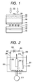
FIG. 1 shows a schematic cross-sectional view of
a photovoltaic device produced in accordance with
this invention. In the same figure, reference numeral
101 denotes a substrate (supporting member), numeral
102 a metal layer, numeral 103 a zinc oxide layer
formed by electrolytic deposition, numerals 105, 106
and 107 semiconductor layers, numeral 108 a
transparent electrode, and numeral 109 a collector
electrode. Further, reference numeral 104 denotes
treatment such as rare gas plasma treatment and
numeral 110 the sun's rays. When a photovoltaic
device is so constructed that light enters from the
transparent substrate side, the layers except the
substrate are formed in reverse order.
Then the constituents of the photovoltaic device
produced in accordance with this invention will be
described.
As the substrate 101 is used resin coated with a
metal layer or an electrically conductive material,
glass, ceramics, etc. The substrate 101 may have fine
unevenness on its surface. A transparent substrate
may be used so that light can enter from the
substrate side. If the substrate is made in a
continuous length, it can accommodate continuous film
formation. Stainless steel and polyimide are
particularly suitable to use for the substrate
because of their flexibility.
The metal layer 102 functions as an electrode
and as a reflecting layer which reflects light having
reached the substrate 101 so that it is reused in the
semiconductor layers. The metal layer is formed of Al,
Cu, Ag or Au by the process such as evaporation,
sputtering, electrolytic deposition or printing.
The metal layer 102 having unevenness on its
surface has the function of extending the optical
path length of reflected light in the semiconductor
layers and increasing short-circuit current. When the
substrate 101 is electrically conductive, the metal
layer need not be formed.
The zinc oxide layer 103 increases the diffused
reflection of incident light and reflected light and
extends the optical path length of the same in the
semiconductor layers. Further, the zinc oxide layer
prevents the elements in the metal layer from
diffusing down or migrating into the semiconductor
layers and the shunt from occurring in the
photovoltaic device. Further, the moderate resistance
of the zinc oxide layer prevents the occurrence of
short-circuit due to the defects in the semiconductor
layers such as pinholes. Preferably the zinc oxide
layer 103 has unevenness on its surface, just as does
the metal layer 102.
The zinc oxide layer 103 is formed by
electrolytic deposition described below. Preferably
the zinc oxide layer is deposited by electrolytic
deposition on a zinc oxide film that has been
provided in advance by sputtering etc., on the metal
layer 102. This produces the effect of improving the
adhesion between the metal layer 102 and the zinc
oxide layer 103.
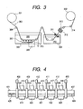
The zinc oxide layer 103 can be formed using,
for example, an apparatus shown in FIG. 2. In the
same figure, reference numeral 201 denotes a
corrosion-resistant container, numeral 202 an aqueous
solution for electrolytic deposition, numeral 203 a
substrate, numeral 204 a counter electrode, numeral
205 a power source, numeral 206 a loading resistor,
numeral 207 a substrate supporting shaft, numeral 208
an electrode supporting shaft, numeral 209 a
substrate branch bone, numeral 210 an electrode
branch bone, numeral 211 an air ejecting opening,
numeral 212 an air ejecting pipe, numeral 213 an air
ejecting pump, and numeral 214 a stirrer.
As the aqueous solution for electrolytic
deposition 202 is used an aqueous solution containing
at least zinc ion and nitric acid ion, and besides,
saccharose or dextrin. The concentration of zinc ion
is preferably 0.002 mol/l to 3.0 mol/l, more
preferably 0.01 mol/l to 1.5 mol/l and optimally 0.05
mol/l to 0.7 mol/l. The concentration of nitric acid
ion is preferably 0.004 mol/l to 6.0 mol/l, more
preferably 0.01 mol/l to 1.5 mol/l and optimally 0.1
mol/l to 1.4 mol/l. The concentration of saccharose
is 1 g/l to 500 g/l and more preferably 3 g/l to 100
g/l and the concentration of dextrin is 0.01 g/l to
10 g/l and more preferably 0.025 g/l to 1 g/l.
Controlling the concentration of each constituent as
above enables the formation of a zinc oxide thin film
having a texture structure suitable for producing
optical confinement effect.
As the electrically conductive substrate 203 is
used the above-described substrate 101 with a metal
layer 102 formed thereon. The counter electrode 204
of the apparatus is a buffed zinc plate and used as
an anode. The zinc content in the zinc plate is
preferably 90% or more and more preferably 99% or
more.
The counter electrode 204 is controlled such
that the current flow is approximately constant. The
current value is preferably 0.1 mA/cm2 to 100 mA/cm2,
more preferably 1 mA/cm2 to 30 mA/cm2 and optimally 3
mA/cm2 to 15 mA/cm2.
As the material for semiconductor layers 105,
106 and 107 is used amorphous or microcrystalline Si,
C or Ge or the alloy thereof. The layers also contain
hydrogen and/or a halogen atom. The preferred content
of such an atom is 0.1 to 40% by atom. The layers may
also contain oxygen, nitrogen, etc. The concentration
of these impurities is preferably 5 × 1019 cm-3 or less.
To provide a p-type semiconductor, elements
classified into the family of column III are added,
whereas to provide an n-type semiconductor, elements
classified into the family of column V are added.
In a stacked cell, it is preferable that the i-type
semiconductor layer of the pin junction has a
wider band gap near the light entering side and a
narrower band gap far away from the light entering
side. It is also preferable that in the inside of the
i layer, the band gap has the minimum on the p-type
layer side relative to the middle of the layer
thickness.
For the doped layer on the light entering side
is suitably used a less light-absorbing crystalline
semiconductor or semiconductor having a wide band gap.
To form semiconductor layers, microwave (MW)
plasma CVD or high frequency (RF, VHF) CVD is
suitably used.
By one technique for the semiconductor
deposition, for example, "an i-type layer with graded
SiGe compositions is formed, where the Ge content is
from 20 to 70% by atom" (refer to Japanese Patent
Application Laid-Open No. H4-119843) can be used.
The transparent electrode 108 can also function
as an anti-reflection coating, if the film thickness
is properly established. The transparent electrode
108 is formed of a material such as ITO, ZnO or In2O3
by evaporation, CVD, spray, spin-on or immersion. The
compound forming the electrode may contain a
substance that changes the electric conductivity.
The collector electrode 109 is provided to
improve the current collecting efficiency. The
processes for forming the electrode include; for
example, a process in which metal of a current
collecting pattern is formed by sputtering using a
mask, a process in which current collecting paste or
solder paste is printed, and a process in which a
metal wire is bonded with a conductive paste
Protective layers are sometimes formed on both
sides of a photovoltaic device depending on the
situation. A reinforcement such as a steel plate may
be used in combination with the collector electrode.
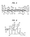
The process of depositing a zinc oxide thin film
will be described using an apparatus shown in FIG. 3.
In the same figure, reference numeral 301 denotes a
delivery roller, numeral 302 a wind-up roller,
numeral 303 a substrate in a continuous length,
numeral 304 a conveying roller, numeral 305 a zinc
oxide depositing tank, numeral 306 a zinc oxide
depositing bath, numeral 307 a counter electrode,
numeral 308 a DC power source, numeral 309 a cleaning
tank, numeral 310 a pure water cleaning bath, numeral
311 a pure water shower, numeral 312 a drying chamber,
numeral 313 an air hole, numeral 314 a meander
correcting roller and numeral 315 an air ejecting
opening.
The substrate in a continuous length 303 wound
around the delivery roller 301 is conveyed via the
path shown in FIG. 3 and wound into the wind-up
roller 302 while its slight deviation is being
corrected by the meander correcting roller 314.
The zinc oxide depositing bath 306 in the zinc
oxide depositing tank 305 is the above-described
aqueous solution for electrolytic deposition that
contains nitric acid ion, zinc ion, and saccharose or
dextrin.
The counter electrode 307 includes one or more
square zinc plates of 99.99% purity. The DC power
source 308 is controlled so that a voltage is applied
across the substrate in a continuous length 303, as a
cathode, and the counter electrode 307, as an anode,
to keep current flow constant.
A uniform zinc oxide thin film in which
anomalous growth is hardly detected can be formed
efficiently by: keeping the temperature of the
aqueous solution for electrolytic deposition at 50°C
or more; and ejecting air through the air ejecting
openings 315 provided on the sidewall of the zinc
oxide depositing tank 305 with an air injection pump
(not shown in the figure) at an ejecting rate of 1 to
100 cm3/h, preferably 5 to 50 cm3/h to stir the
aqueous solution.
A photovoltaic device in accordance with this
invention can be produced employing various types of
production apparatuses and methods. When producing a
single construction type of photovoltaic device shown
in FIG. 1, for example, a production apparatus whose
schematic view is shown in FIG. 5 can be used.
In FIG. 5, reference numerals 501, 502 and 503
denote deposition chambers for depositing n, i, p (or
p, i, n)-type layer by high frequency plasma CVD,
numeral 504 a plasma treatment chamber in which
plasma treatment is carried out with a rare gas or
nitrogen gas by high frequency plasma CVD, and
numerals 505 and 506 a feeding chamber for feeding a
conductive substrate strip and a wind-up chamber for
winding up the same, respectively. The vacuum
chambers of the respective deposition chambers are
connected to each other via gas gates 507, which are
narrow slits where a purge gas such as hydrogen gas
is flowed to prevent the mixing of gases in the
respective deposition chambers.
The substrate strip 508 is, for example, a
conductive substrate strip of stainless steel sheet
0.13 mm thick and 36 cm wide. While the substrate
strip is being wound off from the feeding chamber 505,
continuously conveyed to pass through 4 deposition
chambers 504, 501, 502 and 503 and wound up into the
wind-up chamber 506, an adsorption preventive layer
and a three-layered nip (or pin) structure silicon
non-single crystal semiconductor film for a
photovoltaic device are formed on the surface of the
substrate strip.
Each of the deposition chambers 504, 501 502 and
503 is provided with a heater 510, a material gas
introducing pipe 511 through which a material gas for
depositing semiconductor is introduced into the
deposition chamber from gas feeding means not shown
in the figure, an exhaust pipe 512 for exhausting the
chamber with exhaust means not shown in the figure to
adjust pressure in the chamber to a specified value,
and a discharge electrode 513 for inducing a glow
discharge between a grounded substrate and itself by
supplying high-frequency power from a high-frequency
power source to the gas in the deposition chamber.
And in the deposition chamber 504, plasma treatment
with a rare gas or nitrogen gas is carried out and in
the deposition chambers 501, 502 and 503, n, i, p (or
p, i, n)-type silicon single crystal semiconductor
layers are deposited by plasma CVD.
As described above, the plasma treatment with a
rare gas or nitrogen gas is carried out by plasma CVD,
just as is done the semiconductor deposition;
therefore, the treatment chamber is easy to place in
the front portion of the semiconductor deposition
apparatus. As to the plasma treatment conditions, the
treatment temperature is preferably the same as the
temperature at which the doped layer adjacent to the
zinc oxide layer is deposited and the treatment
pressure is preferably 10 to 2,500 Pa. The making
power is suitably in the range of 0.1 to 2.0 W,
though it varies depending on the frequency of the
high-frequency power source, the distance between the
substrate and the cathode and the pressure in the
chamber.
In the following, this invention will be
described in detail in terms of suitable examples
based on the accompanying drawings. However, it
should be understood that these examples are not
intended to limit the invention.
First, a zinc oxide film was formed using an
electrolytic deposition apparatus shown in FIG. 2. As
the substrate 203, as a cathode, was used a square
stainless steel 430-2D plate with a side 50 mm long
and thickness 0.15 mm which had on its surface a
silver film 2,000 nm thick formed by applying 0.3 A
constant current in an argon atmosphere at 0.399 Pa,
350°C with a sputtering apparatus (ULVAC SBH-2206DE).
As the counter electrode 204, as an anode, was used a
square zinc plate of 99.99% purity with a side 40 mm
long and thickness 1.2 mm. The space between the
counter electrode 204 and the substrate 203 was fixed
to 50 mm.
As the aqueous solution 202 was used 0.15 mol/L
zinc nitrate at 80°C with 12 g/L of saccharose having
been added thereto, and the solution was stirred with
the stirrer 214. Electrolytic deposition was carried
out while carrying 3.0 mA/cm2 of current between the
counter electrode 204 as an anode and the substrate
203 as a cathode, which was grounded. The thickness
of the zinc oxide film formed by the electrolytic
deposition was 3.0 µm.
Then rare gas plasma treatment was performed
using the apparatus shown in FIG. 4.
FIG. 4 is a schematic view showing one form of
the suitable apparatus for forming semiconductor
layers of a photovoltaic device of this invention. In
the same figure, the deposition film forming
apparatus consists mainly of: a load chamber 401, a
rare gas plasma treatment chamber 402, a
microcrystalline silicon i-type layer chamber 403, an
amorphous silicon i-type layer RF chamber 404, an n-type
layer RF chamber 405, a p-type layer RF chamber
406 and an unload chamber 407. The chambers are
separated from each other with gate valves 408, 409,
410, 411, 412 and 413 such that the respective
material gases should not be mixed together.
The rare gas plasma treatment chamber 402
consists of a heater 414 for heating the substrate
and a plasma CVD chamber 419. The microcrystalline
silicon i-type layer chamber 403 consists of a heater
415 for heating the substrate and a plasma CVD
chamber 420. The RF chamber 404 includes an i-type
layer depositing heater 416 and an i-type layer
deposition chamber 421, the RF chamber 405 an n-type
layer depositing heater 417 and an n-type layer
deposition chamber 422, and the RF chamber 406 a p-type
layer depositing heater 418 and a p-type layer
deposition chamber 423.
The substrate is mounted on a substrate holder
425 and moved on a rail 424 with a roller driven from
outside.
The substrate on which a zinc oxide film had
been formed was introduced into the plasma treating
chamber 402, and the treatment chamber was evacuated
to a pressure of 100 Pa or less by an evacuation
system not shown in the figure. After the evacuation,
helium gas was introduced into the chamber while
controlling its flow with a mass flow controller.
Then the treatment chamber was evacuated to a
pressure of 300 Pa while controlling the pressure in
its inside. Plasma treatment was carried out for two
minutes while supplying high-frequency power of 13.56
MHz and 1 W/cm2 power density from a power source not
shown in the figure via matching equipment to a
discharge electrode provided in the deposition
chamber 402. Then, the substrate was taken out from
the plasma treatment chamber 402, and total
reflectance and diffused reflectance, water content
in the deposited film and electrical resistance were
measured for the substrate.
The total reflectance and diffused reflectance
were determined in the light wavelength region of 400
nm to 1,200 nm with a spectrometer (V-570, made by
JASCO Corporation). The water content in the film was
determined with a Karl Fischer moisture titrator
(MKC-510, made by Kyoto Electronics manufacturing Co.,
Ltd.). And the electric resistance was determined in
such a manner as to first form an upper electrode by
evaporating metals of Cr and Au in this order onto
the above zinc oxide film with a vacuum evaporation
apparatus using a mask 0.25 cm2 in size and measure
the electric resistance between the stainless steel
substrate and the upper electrode. Since the
measurement system, including the measurement pointer,
itself had a circuit resistance of about 0.1 Ωcm2,
the measurement of the electric resistance may have
an error equivalent of such resistance.
A zinc oxide film was formed on a substrate in
the same manner as in Example 1, and then the
substrate 602 was introduced into a heat treatment
chamber 601 shown in FIG. 6 and dehydrated for 10
minutes while increasing the temperature of the
object to be treated (substrate) from room
temperature up to 200°C in increments of 2.0°C/min and,
after completing the temperature increase,
controlling the same with a heater output system 606
so as to keep the object to be treated at 200°C. In
FIG. 6, reference numeral 603 denotes a heater,
numeral 604 a treatment chamber monitoring
thermocouple, numeral 605 a heater output regulator,
numeral 607 a nitrogen gas mass flow controller,
numeral 608 an oxygen gas mass flow controller,
numeral 609 a pressure regulating valve and numeral
610 an evacuating pump.
After completing the dehydration treatment, the
heater output was turned off and the substrate was
cooled to room temperature while keeping the oxygen-nitrogen
flow rate ratio such that the partial
pressure of oxygen is 2%. After cooled, the substrate
with a zinc oxide film formed thereon was introduced
into the plasma treatment chamber 402 shown in FIG. 4,
and the treatment chamber was evacuated with a
evacuating system not shown in the figure to a
pressure of 100 Pa or less. After the evacuation,
helium gas was introduced while controlling its flow
with a mass flow controller. Then the treatment
chamber was evacuated while controlling the pressure
inside the chamber to be 300 Pa. Plasma treatment was
carried out for two minutes while supplying high-frequency
power of 13.56 MHz and 1 W/cm2 power density
from a power source not shown in the figure via
matching equipment to a discharge electrode 419
provided in the deposition chamber 402. Then, the
substrate was taken out from the plasma treatment
chamber 402, and total reflectance and diffused
reflectance, water content in the deposited film and
electrical resistance were measured for the substrate
in the same manner as in Example 1.
A silver film 2,000 nm thick was formed on the
same substrate as used in Example 1 by applying 0.3 A
constant current in an argon atmosphere at 0.399 Pa,
350°C with a sputtering apparatus (ULVAC SBH-2206DE).
And 0.3 A constant current was applied to the zinc
oxide target with the same sputtering apparatus, to
deposit zinc oxide 3.0 µm. Then, the substrate was
taken out, and total reflectance and diffused
reflectance, water content in the deposited film and
electrical resistance were measured for the substrate
in the same manner as in Example 1.
The zinc oxide film was formed on a substrate in
the same manner as in Example 1, but heat drying and
rare gas plasma treatment were not performed. Then,
total reflectance and diffused reflectance, water
content in the deposited film and electrical
resistance were measured for the substrate in the
same manner as in Example 1.
The zinc oxide film was formed on a substrate in
the same manner as in Example 1, and then the
substrate 602 was introduced into a heat treatment
chamber 601 shown in FIG. 6 and dehydrated for 10
minutes while increasing the temperature of the
object to be treated (substrate) from room
temperature up to 200°C in increments of 2.0°C/min and,
after completing the temperature increase,
controlling the same with a heater output system 606
so as to keep the object to be treated at 200°C.
After completing the treatment, the heater
output was turned off and the substrate was cooled to
room temperature while keeping the oxygen-nitrogen
flow rate ratio such that the partial pressure of
oxygen is 2%. After cooled, the substrate 602 was
taken out from the heat treatment chamber 601, and
total reflectance and diffused reflectance, water
content in the deposited film and electrical
resistance were measured for the substrate in the
same manner as in Example 1.
Table 1 shows the measured results of Examples 1,
2 and Comparative Examples 1, 2 and 3.
| Zinc Oxide Depositing Process | Drying Process | Reflectance | Water Content (mol/ cm2) | Electric Resistance (Ω/cm2) | |||
| Heating | Rare Gas Plasma | Total Reflection | Diffused Reflection | ||||
| Comparative Example 1 | Sputtering | - | - | 90 | 86 | 0.8×10⁻³ | 0.2-0.3 |
| Comparative Example 2 | Electrolytic Deposition | - | - | 93 | 90 | 8.0×10⁻³ | 9.0-10.0 |
| Comparative Example 3 | O | - | 92 | 89 | 1.9×10⁻³ | 0.3-0.4 | |
| Example 1 | - | O | 92 | 89 | 1.9×10⁻³ | 0.3-0.5 | |
| Example 2 | O | O | 92 | 89 | 1.1×10⁻³ | 0.2-0.3 |
As is apparent from the results shown in Table 1,
for the zinc oxide film formed by electrolytic
deposition and in the as-formed state (Comparative
Example 2), its total reflectance and diffused
reflectance were high compared with the zinc oxide
film formed by sputtering, and the water content in
the film was about 10 times as much as that of the
zinc oxide film formed by sputtering and the electric
resistance was high. Thus, even if a photovoltaic
device is formed on such a zinc oxide film, the
device cannot be expected to have desired
characteristics.
For the zinc oxide films of Comparative Example
3, Example 1 and Example 2, their total reflectance
and diffused reflectance were good, even after drying,
compared with the zinc oxide film formed by
sputtering. Their water content was a little larger
than that of the zinc oxide film formed by sputtering,
but the electric resistance obtained was almost the
same as that of the zinc oxide film formed by
sputtering.
Then semiconductor layers were formed on each of
the substrates obtained in Comparative Example 1,
Comparative Example 3, Example 1 and Example 2 under
the deposition conditions given for each layer as
shown in table 2 with an apparatus shown in FIG. 4.
| Deposition Gas (cm3/min (normal)) | Power Density (W/cm2) | Pressure (Pa) | substrate Temperature (°C) | Film Thickness (nm) | ||||||
| SiH4 | H2 | PH3 (2% H dilution) | BF3 (2% H dilution) | RF | VHF | |||||
| First Photovoltaic Device | N2 | 1 | 50 | 0.5 | 0.04 | 180 | 225 | 20 | ||
| I2 | 25 | 800 | 0.2 | 40 | 250 | 1,800 | ||||
| P2 | 0.025 | 35 | 1 | 1.2 | 270 | 165 | 5 | |||
| Second Photovoltaic Device | N1 | 1 | 50 | 0.5 | 0.04 | 180 | 225 | 20 | ||
| I1 | 2 | 50 | 0.05 | 150 | 210 | 400 | ||||
| P1 | 0.025 | 35 | 1 | 1.2 | 270 | 165 | 5 |
First, each substrate was set in the substrate
holder 425 and set on the rail 424 of the load
chamber 401. Then the load chamber 401 was evacuated
to a vacuum degree of several hundreds Pa or less.
Then, the gate valves 408, 409, 410 and 411 were
opened and the substrate holder 425 was moved to the
n-type layer deposition chamber 422 of the chamber
405. An n-type layer was deposited to a predetermined
thickness with a predetermined material gas while
keeping the gate valves 408, 409, 410, 411, 412 and
413 closed. After fully evacuating the chamber 405,
the substrate holder 425 was moved to the deposition
chamber 403 while keeping the gate valves 410 and 411
opened, and then the gate valves were closed. The
substrate was heated with the heater 415 to a
predetermined substrate temperature, and a
microcrystalline silicon i-type layer was deposited
on the substrate to a predetermined thickness by
introducing a required amount of predetermined
material gas into the chamber 403, evacuating the
chamber 403 to a predetermined vacuum degree,
introducing a predetermined microwave energy or VHF
energy into the deposition chamber 420 to induce
plasma.
Then, the chamber 403 was fully evacuated, the
substrate holder 425 was moved from the chamber 403
to the p-type layer deposition chamber 423 of the
chamber 406 while keeping the gate valves 410, 411,
412 open, and the substrate was heated with the
heater 418 to a desired substrate temperature. A p-type
layer was deposited to a desired thickness by
supplying predetermined flow rate of material gas for
p-type layer deposition and introducing RF energy
into the deposition chamber 423 while keeping the
chamber at a predetermined vacuum degree.
Subsequently, on the substrate on which a first
photovoltaic device had been formed in the manner as
described above, a pin-type amorphous Si:H
photovoltaic device was formed as a second
photovoltaic device in such a manner as described
below.
An n-type layer was deposited under
predetermined conditions in the same manner as
described above. After fully evacuating the chamber
405, the substrate holder 425 was moved to the
deposition chamber 404 while keeping the gate valve
411 opened, and then the gate valve was closed. The
substrate was heated with the heater 416 to a
predetermined substrate temperature, and an amorphous
Si:H i-type layer was deposited on the substrate to a
predetermined thickness in accordance with Table 2,
while adjusting the deposition time, by introducing a
required amount of predetermined material gas into
the chamber 404, evacuating the chamber 404 to a
predetermined vacuum degree, introducing a
predetermined microwave energy into the deposition
chamber 421 to induce plasma. Then, the chamber 404
was fully evacuated, and the substrate holder 425 was
moved from the chamber 421 to the chamber 423 while
keeping the gate valves 411, 412 open. And a p-type
layer was deposited to a predetermined thickness
under predetermined conditions in the same manner as
above.
Then, the deposition chamber 423 was evacuated
in the same manner as above, the gate valve 413 was
opened, and the substrate holder 425 in which the
substrate with semiconductor layers deposited thereon
had been set was moved to the unload chamber 407. The
substrate holder 425 was taken out from the unload
chamber 407 in the same manner as above.
Then the substrate was mounted on the surface of
the anode of a DC magnetron sputtering apparatus, the
surrounding of the sample was shielded with a
stainless steel mask, and on the region of the center
portion 40 mm × 40 mm, tin indium oxide was deposited
as a transparent electrode by sputtering using a
target made up of 10% by weight of tin oxide and 90%
by weight of indium oxide.
The deposition was performed so as to provide a
film of 70 nm in about 100 seconds under the
following conditions: substrate temperature 170°C;
flow rates of argon, as an inert gas, 50 cm3/min
(normal) and oxygen gas 0.5 cm3/min (normal); pressure
in the deposition chamber 300 mPa; and making power
per target unit area 0.2 W/cm2. The film was allowed
to have a predetermined thickness by calibrating in
advance the relation between the deposition time and
the film thickness under the same conditions.
The current-voltage characteristics of the
resultant samples were measured, while irradiating
the samples with light at a spectrum of AM 1.5 and an
intensity of 100 mW/cm2, with YSS-150 made by
Yamashita Denso Corporation. The short-circuit
current density (Jsc (mA/cm2)), open circuit voltage
(Voc (V)), fill factor (FF) and photoelectric
conversion efficiency (η (%)) were obtained for each
sample from the measured current-voltage
characteristics. The characteristic values were
expressed in terms of the ratio of the values of each
sample to those of the sample of comparative Example
1, which was formed by sputtering, and are summarized
in Table 3.
| Jsc | FF | Voc | Eff. | |
| Comparative Example 3/ Comparative Example 1 | 0.988 | 0.972 | 0.995 | 0.956 |
| Example 1/ Comparative Example 1 | 1.057 | 0.997 | 0.999 | 1.053 |
| Example 2/ Comparative Example 1 | 1.060 | 0.998 | 1.000 | 1.058 |
As is apparent from the results shown in Table 3,
in the sample of Comparative Example 3, the total
reflection and diffused reflection were both good
compared with those of the sample of Comparative
Example 1, but Jsc and FF were inferior to those of
the sample of Comparative Example 1. The visual
observation of the surface of the photovoltaic device
confirmed a little peeling of the semiconductor
layers.
In the samples of Examples 1 and 2, the results
were good compared with those of the sample of
Comparative Example 1. And no peeling was observed
visually.
Reliability test was also conducted as follows.
Each sample was introduced into a high-temperature
and high-humidity tank and kept at a temperature of
+85°C and a relative humidity of 85%. While testing,
backward bias voltage -0.85 V was continued to apply
to each sample for 20 hours. Then the sample was
taken out from the tank and fully air dried and
cooled, and the voltage-current characteristics were
measured. The characteristics were expressed in terms
of the relative values to the initial values and are
shown in Table 4.
| Jsc | FF | Voc | Eff. | Rsh | |
| Comparative Example 3 | 0.851 | 0.996 | 0.945 | 0.801 | 0.664 |
| Example 1 | 1.000 | 0.996 | 1.003 | 0.999 | 0.998 |
| Example 2 | 0.999 | 0.997 | 1.003 | 0.999 | 0.999 |
In the samples of Examples 1 and 2, the
deterioration in shunt resistance was hardly observed
in the reliability test. However, in the sample of
Comparative Example 3, substantial deterioration in
both shunt resistance and photoelectric conversion
efficiency, which might be caused by the peeling of
the semiconductor layers, was observed.
Then, using the apparatus shown in FIG. 4, first
and second photovoltaic devices were formed on the
substrates obtained in Comparative Examples 1 and 3
and Examples 1 and 2 under the given deposition
conditions shown in Table 5 in the same manner as
above, except that an adsorption preventive layer was
formed in the n-type layer deposition chamber 422 of
the chamber 405.
| Deposition Gas (cm3/min(normal)) | Power Density (W/cm2) | Pressure (Pa) | Substrate Temperature (°C) | Film Thickness (nm) | ||||||
| SiH4 | H2 | PH3 (2% H dilution) | BF3 (2% H dilution) | RF | VHF | |||||
| Adsorption Preventive Layer | N3 | 1 | 150 | 0.05 | 0.06 | 180 | 225 | 10 | ||
| First Photovoltaic Device | N2 | 1 | 50 | 0.5 | 0.04 | 180 | 225 | 20 | ||
| I2 | 25 | 800 | 0.2 | 40 | 250 | 1,800 | ||||
| P2 | 0.025 | 35 | 1 | 1.2 | 270 | 165 | 5 | |||
| Second Photovoltaic Device | N1 | 1 | 50 | 0.5 | 0.04 | 180 | 225 | 20 | ||
| I1 | 2 | 50 | 0.05 | 150 | 210 | 400 | ||||
| P1 | 0.025 | 35 | 1 | 1.2 | 270 | 165 | 5 |
The current-voltage characteristics of the
resultant samples were measured, while irradiating
the samples with light at a spectrum of AM 1.5 and an
intensity of 100 mW/cm2, with YSS-150 made by
Yamashita Denso Corporation. The short-circuit
current density (Jsc (mA/cm2)), open circuit voltage
(Voc (V)), fill factor (FF) and photoelectric
conversion efficiency (η (%)) were obtained for each
sample from the measured current-voltage
characteristics. The characteristic values were
expressed in terms of the ratio of the values of each
sample having an adsorption preventive film to those
of the sample having no adsorption preventive film
and are summarized in Table 6. As is apparent from
the results shown in Table 6, in the samples of
Examples 1 and 2, which were given rare gas plasma
treatment, Eff was improved due to the improvement in
Jsc. And no peeling was observed visually.
| Adsorption Preventive Layer Presence/ Absence | Jsc | FF | Voc | Eff. |
| Example 1 | 1.050 | 0.998 | 0.997 | 1.045 |
| Example 2 | 1.055 | 0.999 | 0.999 | 1.053 |
| Comparative Example 1 | 1.003 | 0.999 | 1.000 | 1.002 |
| Comparative Example 2 | 1.001 | 0.999 | 1.000 | 1.000 |
| Comparative Example 3 | 1.010 | 0.998 | 1.000 | 1.008 |
Reliability test was also conducted as follows.
Each sample was introduced into a high-temperature
and high-humidity tank and kept at a temperature of
+85°C and a relative humidity of 85%. While testing,
backward bias voltage -0.85 V was continued to apply
to each sample for 20 hours. Then the sample was
taken out from the tank and fully air dried and
cooled, and the voltage-current characteristics were
measured. The characteristics were expressed in terms
of the relative values to the initial values and are
shown in Table 7.
In the samples of Examples 1 and 2, the
deterioration in shunt resistance was hardly observed
in the reliability test. However, in the sample of
Comparative Example 3, substantial deterioration in
both shunt resistance and photoelectric conversion
efficiency, which might be caused by the peeling of
the semiconductor layers, was observed.
| Jsc | FF | Voc | Eff. | Rsh | |
| Comparative Example 3 | 0.853 | 0.996 | 0.945 | 1.000 | 0.665 |
| Example 1 | 1.000 | 0.996 | 1.002 | 0.998 | 0.998 |
| Example 2 | 0.999 | 0.998 | 1.002 | 0.999 | 0.999 |
The results so far show that a photovoltaic
device produced using a substrate whose zinc oxide
layer is formed by electrolytic deposition and
subjected to rare gas plasma treatment is high in
photoelectric conversion efficiency, excellent in
adhesion among the semiconductor layers and high in
reliability. Further, a photovoltaic device produced
using a substrate on which an adsorption preventive
layer is formed after the plasma treatment has
further improved photoelectric conversion efficiency
and is higher in reliability.
In this example, plasma treatment with a rare
gas was given to a substrate on which a zinc oxide
film had been formed by electrolytic deposition and
then photovoltaic devices having a nip structure were
continuously produced using a production apparatus
shown in FIG. 5. The production conditions are shown
in FIG. 8.
| | ||||
| 504 | 501 | 502 | 503 | |
| Rare Gas Plasma-Treatment | n-Type Amorphous Silicon | i-Type Microcrystalline Silicon | p-Type Microcrystalline Silicon | |
| Discharge Frequency (MHz) | 13.56 | 13.56 | 60 | 13.56 |
| Thickness of Semi-conductor | - | 20 | 1,500 | 10 |
| Gas (sccm) | ||||
| SiH4 | - | 10 | 150 | 20 |
| H2 | - | 1,000 | 4,000 | 5,000 |
| SiF4 | - | - | 400 | - |
| PH3 | - | 0.5 | - | - |
| BF3 | - | - | - | 5 |
| He | 1,000 | - | - | - |
| Substrate Temperature (°C) | 250 | 250 | 250 | 200 |
| Discharge Power (W) | 150 | 100 | 3,000 | 2,500 |
| Deposition Pressure (Pa) | 550 | |||
| Conveying Speed (cm/min) | 100 |
In the following the process of photovoltaic
device production will be described in a step by step
manner.
This example is different from Example 3 in that
rare gas plasma treatment was not performed.
Specifically, in this example, semiconductor layers
were formed in the same manner as in Example 3,
except that the substrate 501 was passed through the
rare gas plasma treatment chamber 504 of the
production apparatus shown in FIG. 5 where He gas was
introduced through the material gas introducing pipe
511 and high-frequency power was not supplied to the
discharge electrode 513. Excepting the above point,
photovoltaic devices 30 cm × 30 cm with an n-i-p
configuration were produced in the same manner as in
Example 3.
The characteristic values were expressed in
terms of the ratio of the values of the sample of
Comparative Example 4 to those of the sample of
Example 3 (Comparative Example 4/Example 3) and are
summarized in Table 9.
| Jsc | FF | Voc | Eff. | |
| Comparative Example 4 /Example 3 | 0.998 | 0.922 | 1.000 | 0.920 |
Reliability test was also conducted as follows.
Each sample was introduced into a high-temperature
and high-humidity tank and kept at a temperature of
+85°C and a relative humidity of 85%. While testing,
backward bias voltage -0.85 V was continued to apply
to each sample for 20 hours. Then the sample was
taken out from the tank and fully air dried and
cooled, and the voltage-current characteristics were
measured. The characteristics were expressed in terms
of the relative values to the initial values and are
shown in Table 10.
| Jsc | FF | Vbc | Eff. | |
| Example 3 | 1.001 | 0.996 | 1.003 | 1.000 |
| Comparative Example 4 | 0.965 | 0.980 | 1.002 | 0.947 |
In the sample of comparative example 4, its FF
(fill factor) substantially deteriorated, compared
with the sample of Example 1, due to insufficient
removal of water in the zinc oxide film. In the
reliability test, in the sample of Comparative
Example 4, deterioration in photoelectric conversion
efficiency was observed due to the substantial
deterioration in Jsc. And a large number of peeling
portions were observed visually, which may be the
cause of the deterioration in Jsc.
The results show that a photovoltaic device
produced on a substrate whose zinc oxide layer is
formed by electrolytic deposition and subjected to
rare gas plasma treatment is good in initial
photoelectric conversion efficiency and high in
reliability.
There is disclosed a method of producing a
photovoltaic device, characterized in that it
includes steps of: a step of forming a zinc oxide
layer on a substrate at least by electrolytic
deposition; subjecting the zinc oxide layer to any
one treatment selected from the group consisting of
plasma treatment with a rare gas or nitrogen gas, ion
irradiation, light irradiation and electromagnetic
irradiation; and forming on the zinc oxide layer a
semiconductor layer that are made up of a non-single
crystal silicon material containing hydrogen and have
at least one p-i-n junction.
Claims (7)
- A method of producing a photovoltaic device, comprising steps of:forming a zinc oxide layer on a substrate at least by electrolytic deposition;subjecting the zinc oxide layer to any one treatment selected from the group consisting of plasma treatment with a rare gas or nitrogen gas, ion irradiation, light irradiation and electromagnetic irradiation; andforming on the zinc oxide layer a semiconductor layer comprising a non-single crystal silicon material containing hydrogen and having at lease one p-i-n junction.
- The method of producing a photovoltaic device according to claim 1, wherein the treatment is a rare gas plasma treatment using at least one rare gas selected from the group consisting of He, Ne, Ar, Kr and Xe.
- The method of producing a photovoltaic device according to claim 1, wherein before forming the zinc oxide layer, another zinc oxide layer is formed on the substrate by sputtering and used as an underlying layer.
- The method of producing a photovoltaic device according to claim 1, wherein the average thickness of the zinc oxide layer is from 10 nm to 5 µm inclusive.
- The method of producing a photovoltaic device according to claim 1, wherein the zinc oxide layer transmits 50% or more of light with a wavelength of 800 nm.
- The method of producing a photovoltaic device according to claim 1, wherein the zinc oxide layer has a resistivity lower than that of a p- or n-type semiconductor layer provided adjacent to the zinc oxide layer.
- The method of producing a photovoltaic device according to claim 1, wherein an adsorption preventive layer is provided between the zinc oxide layer and a p- or n-type semiconductor layer provided adjacent to the zinc oxide layer.
Applications Claiming Priority (4)
| Application Number | Priority Date | Filing Date | Title |
|---|---|---|---|
| JP2003085880 | 2003-03-26 | ||
| JP2003085880 | 2003-03-26 | ||
| JP2004066561 | 2004-03-10 | ||
| JP2004066561A JP2004311965A (en) | 2003-03-26 | 2004-03-10 | Method for manufacturing photovoltaic element |
Publications (1)
| Publication Number | Publication Date |
|---|---|
| EP1463128A2 true EP1463128A2 (en) | 2004-09-29 |
Family
ID=32829045
Family Applications (1)
| Application Number | Title | Priority Date | Filing Date |
|---|---|---|---|
| EP04007128A Withdrawn EP1463128A2 (en) | 2003-03-26 | 2004-03-24 | Method of producing photovoltaic device |
Country Status (5)
| Country | Link |
|---|---|
| US (1) | US20040191950A1 (en) |
| EP (1) | EP1463128A2 (en) |
| JP (1) | JP2004311965A (en) |
| CN (1) | CN1534799A (en) |
| AU (1) | AU2004201229A1 (en) |
Cited By (1)
| Publication number | Priority date | Publication date | Assignee | Title |
|---|---|---|---|---|
| US10186619B2 (en) | 2009-11-20 | 2019-01-22 | Semiconductor Energy Laboratory Co., Ltd. | Method for manufacturing semiconductor device |
Families Citing this family (28)
| Publication number | Priority date | Publication date | Assignee | Title |
|---|---|---|---|---|
| JP2006269607A (en) * | 2005-03-23 | 2006-10-05 | Canon Inc | Photovoltaic element manufacturing method |
| JP5037808B2 (en) | 2005-10-20 | 2012-10-03 | キヤノン株式会社 | Field effect transistor using amorphous oxide, and display device using the transistor |
| US20080308147A1 (en) * | 2007-06-12 | 2008-12-18 | Yiwei Lu | Rear electrode structure for use in photovoltaic device such as CIGS/CIS photovoltaic device and method of making same |
| US8071179B2 (en) | 2007-06-29 | 2011-12-06 | Stion Corporation | Methods for infusing one or more materials into nano-voids if nanoporous or nanostructured materials |
| US7687300B2 (en) * | 2007-10-22 | 2010-03-30 | Applied Materials, Inc. | Method of dynamic temperature control during microcrystalline SI growth |
| KR100870837B1 (en) * | 2008-03-04 | 2008-11-28 | 한국철강 주식회사 | Water removal method of zinc oxide thin film |
| US8044594B2 (en) * | 2008-07-31 | 2011-10-25 | Advanced Energy Industries, Inc. | Power supply ignition system and method |
| US20100089318A1 (en) * | 2008-09-12 | 2010-04-15 | Ovshinsky Stanford R | Remote Plasma Apparatus for Manufacturing Solar Cells |
| US7947524B2 (en) | 2008-09-30 | 2011-05-24 | Stion Corporation | Humidity control and method for thin film photovoltaic materials |
| US8741689B2 (en) * | 2008-10-01 | 2014-06-03 | Stion Corporation | Thermal pre-treatment process for soda lime glass substrate for thin film photovoltaic materials |
| US20110018103A1 (en) * | 2008-10-02 | 2011-01-27 | Stion Corporation | System and method for transferring substrates in large scale processing of cigs and/or cis devices |
| US8395078B2 (en) | 2008-12-05 | 2013-03-12 | Advanced Energy Industries, Inc | Arc recovery with over-voltage protection for plasma-chamber power supplies |
| EP2648209B1 (en) | 2009-02-17 | 2018-01-03 | Solvix GmbH | A power supply device for plasma processing |
| US8241943B1 (en) | 2009-05-08 | 2012-08-14 | Stion Corporation | Sodium doping method and system for shaped CIGS/CIS based thin film solar cells |
| US8372684B1 (en) | 2009-05-14 | 2013-02-12 | Stion Corporation | Method and system for selenization in fabricating CIGS/CIS solar cells |
| US8507786B1 (en) | 2009-06-27 | 2013-08-13 | Stion Corporation | Manufacturing method for patterning CIGS/CIS solar cells |
| KR101460868B1 (en) | 2009-07-10 | 2014-11-11 | 가부시키가이샤 한도오따이 에네루기 켄큐쇼 | Semiconductor device |
| KR101127491B1 (en) * | 2009-07-29 | 2012-03-23 | 삼성코닝정밀소재 주식회사 | Method for manufacturing substrate of photovoltaic cell |
| JP5224470B2 (en) * | 2009-07-31 | 2013-07-03 | 国立大学法人東北大学 | Photoelectric conversion member |
| US8398772B1 (en) | 2009-08-18 | 2013-03-19 | Stion Corporation | Method and structure for processing thin film PV cells with improved temperature uniformity |
| US8859880B2 (en) * | 2010-01-22 | 2014-10-14 | Stion Corporation | Method and structure for tiling industrial thin-film solar devices |
| US8142521B2 (en) * | 2010-03-29 | 2012-03-27 | Stion Corporation | Large scale MOCVD system for thin film photovoltaic devices |
| US9096930B2 (en) | 2010-03-29 | 2015-08-04 | Stion Corporation | Apparatus for manufacturing thin film photovoltaic devices |
| US8361229B2 (en) * | 2010-04-22 | 2013-01-29 | Primestar Solar, Inc. | Seal configuration for a system for continuous deposition of a thin film layer on a substrate |
| US8461061B2 (en) | 2010-07-23 | 2013-06-11 | Stion Corporation | Quartz boat method and apparatus for thin film thermal treatment |
| US8552665B2 (en) | 2010-08-20 | 2013-10-08 | Advanced Energy Industries, Inc. | Proactive arc management of a plasma load |
| CN103173829A (en) * | 2013-04-19 | 2013-06-26 | 济南大学 | Method for preparing cadmium telluride semiconductor thin film by electrochemical deposition |
| KR102689097B1 (en) * | 2019-08-30 | 2024-07-25 | 케이힌 람테크 가부시키가이샤 | Laminated structure, and method of manufacturing the laminated structure |
Family Cites Families (21)
| Publication number | Priority date | Publication date | Assignee | Title |
|---|---|---|---|---|
| US5180434A (en) * | 1991-03-11 | 1993-01-19 | United Solar Systems Corporation | Interfacial plasma bars for photovoltaic deposition apparatus |
| US5769963A (en) * | 1995-08-31 | 1998-06-23 | Canon Kabushiki Kaisha | Photovoltaic device |
| DE69702277T2 (en) * | 1996-03-06 | 2001-03-01 | Canon K.K., Tokio/Tokyo | A method of manufacturing a thin zinc oxide film and a method of manufacturing a substrate of a semiconductor device, and a method of manufacturing a photoelectric conversion device using this film |
| US6172296B1 (en) * | 1996-05-17 | 2001-01-09 | Canon Kabushiki Kaisha | Photovoltaic cell |
| US6123824A (en) * | 1996-12-13 | 2000-09-26 | Canon Kabushiki Kaisha | Process for producing photo-electricity generating device |
| JPH10335684A (en) * | 1997-05-30 | 1998-12-18 | Canon Inc | Method for manufacturing photoelectric converter |
| JPH1146006A (en) * | 1997-07-25 | 1999-02-16 | Canon Inc | Photovoltaic element and method for manufacturing the same |
| JPH11233801A (en) * | 1998-02-17 | 1999-08-27 | Canon Inc | Method for forming microcrystalline silicon film and photovoltaic element |
| JP4208281B2 (en) * | 1998-02-26 | 2009-01-14 | キヤノン株式会社 | Multilayer photovoltaic device |
| US6303945B1 (en) * | 1998-03-16 | 2001-10-16 | Canon Kabushiki Kaisha | Semiconductor element having microcrystalline semiconductor material |
| US6344608B2 (en) * | 1998-06-30 | 2002-02-05 | Canon Kabushiki Kaisha | Photovoltaic element |
| US6472248B2 (en) * | 1999-07-04 | 2002-10-29 | Canon Kabushiki Kaisha | Microcrystalline series photovoltaic element and process for fabrication of same |
| JP4171162B2 (en) * | 2000-05-30 | 2008-10-22 | 三洋電機株式会社 | Photovoltaic element and manufacturing method thereof |
| JP2002134772A (en) * | 2000-10-24 | 2002-05-10 | Canon Inc | Silicon based thin film and photovoltaic device |
| JP2002206168A (en) * | 2000-10-24 | 2002-07-26 | Canon Inc | Method for forming silicon-based thin film, method for forming silicon-based semiconductor layer, and photovoltaic element |
| JP2002237606A (en) * | 2000-12-04 | 2002-08-23 | Canon Inc | Solar cell substrate, solar cell using the same, and method of manufacturing solar cell |
| JP2002305315A (en) * | 2001-01-31 | 2002-10-18 | Canon Inc | Method of forming semiconductor device and semiconductor device |
| US6706336B2 (en) * | 2001-02-02 | 2004-03-16 | Canon Kabushiki Kaisha | Silicon-based film, formation method therefor and photovoltaic element |
| US6858308B2 (en) * | 2001-03-12 | 2005-02-22 | Canon Kabushiki Kaisha | Semiconductor element, and method of forming silicon-based film |
| JP2003007629A (en) * | 2001-04-03 | 2003-01-10 | Canon Inc | Silicon-based film forming method, silicon-based film, and semiconductor element |
| JP2003046496A (en) * | 2001-07-31 | 2003-02-14 | Canon Inc | Information management method, information management system and processing device |
-
2004
- 2004-03-10 JP JP2004066561A patent/JP2004311965A/en not_active Withdrawn
- 2004-03-23 US US10/806,157 patent/US20040191950A1/en not_active Abandoned
- 2004-03-24 AU AU2004201229A patent/AU2004201229A1/en not_active Abandoned
- 2004-03-24 EP EP04007128A patent/EP1463128A2/en not_active Withdrawn
- 2004-03-25 CN CNA2004100085877A patent/CN1534799A/en active Pending
Cited By (1)
| Publication number | Priority date | Publication date | Assignee | Title |
|---|---|---|---|---|
| US10186619B2 (en) | 2009-11-20 | 2019-01-22 | Semiconductor Energy Laboratory Co., Ltd. | Method for manufacturing semiconductor device |
Also Published As
| Publication number | Publication date |
|---|---|
| JP2004311965A (en) | 2004-11-04 |
| AU2004201229A1 (en) | 2004-10-14 |
| CN1534799A (en) | 2004-10-06 |
| US20040191950A1 (en) | 2004-09-30 |
Similar Documents
| Publication | Publication Date | Title |
|---|---|---|
| EP1463128A2 (en) | Method of producing photovoltaic device | |
| US7282132B2 (en) | Zinc oxide film treatment method and method of manufacturing photovoltaic device utilizing the same | |
| EP0895291B1 (en) | Photovoltaic element and method of producing the same | |
| US6331672B1 (en) | Photovoltaic cell and method for manufacturing the same | |
| US6576112B2 (en) | Method of forming zinc oxide film and process for producing photovoltaic device using it | |
| EP1463126A2 (en) | Stacked photovoltaic device | |
| US6812499B2 (en) | Silicon-based film and photovoltaic element | |
| US7445952B2 (en) | Method of forming laminate and method of manufacturing photovoltaic device | |
| Takano et al. | Light-weight and large-area solar cell production technology | |
| US6653165B2 (en) | Methods of forming semiconductor element, and semiconductor elements | |
| KR101179443B1 (en) | Protective layer for large-scale production of thin-film solar cells | |
| JP3027670B2 (en) | Photovoltaic element | |
| US20030085129A1 (en) | Method of forming zinc oxide film, method of producing semiconductor element substrate using same, and method of producing photovoltaic element | |
| US20050150773A1 (en) | Method for forming deposition film and method for producing photovoltaic device | |
| JP2006269607A (en) | Photovoltaic element manufacturing method | |
| JP2000004036A (en) | Method for forming microcrystalline semiconductor layer and photovoltaic element | |
| JP2001358350A (en) | Photovoltaic element | |
| JP2002134773A (en) | Photovoltaic element | |
| JP4012106B2 (en) | Method for forming photovoltaic element | |
| JP2713847B2 (en) | Thin film solar cell | |
| JPH0969640A (en) | Photovoltaic element | |
| JPH11274540A (en) | Photovoltaic element and method for manufacturing the same | |
| JP3017421B2 (en) | Photovoltaic element | |
| JP3072831B2 (en) | Photovoltaic element | |
| JP2003158085A (en) | Deposition film formation method |
Legal Events
| Date | Code | Title | Description |
|---|---|---|---|
| PUAI | Public reference made under article 153(3) epc to a published international application that has entered the european phase |
Free format text: ORIGINAL CODE: 0009012 |
|
| AK | Designated contracting states |
Kind code of ref document: A2 Designated state(s): AT BE BG CH CY CZ DE DK EE ES FI FR GB GR HU IE IT LI LU MC NL PL PT RO SE SI SK TR |
|
| AX | Request for extension of the european patent |
Extension state: AL LT LV MK |
|
| STAA | Information on the status of an ep patent application or granted ep patent |
Free format text: STATUS: THE APPLICATION HAS BEEN WITHDRAWN |
|
| 18W | Application withdrawn |
Effective date: 20060713 |