EP1450413A2 - Adhesive type LED lead frame - Google Patents
Adhesive type LED lead frame Download PDFInfo
- Publication number
- EP1450413A2 EP1450413A2 EP03009573A EP03009573A EP1450413A2 EP 1450413 A2 EP1450413 A2 EP 1450413A2 EP 03009573 A EP03009573 A EP 03009573A EP 03009573 A EP03009573 A EP 03009573A EP 1450413 A2 EP1450413 A2 EP 1450413A2
- Authority
- EP
- European Patent Office
- Prior art keywords
- base
- positive pole
- crystal
- lead frame
- joint
- Prior art date
- Legal status (The legal status is an assumption and is not a legal conclusion. Google has not performed a legal analysis and makes no representation as to the accuracy of the status listed.)
- Withdrawn
Links
Images


Classifications
-
- H—ELECTRICITY
- H10—SEMICONDUCTOR DEVICES; ELECTRIC SOLID-STATE DEVICES NOT OTHERWISE PROVIDED FOR
- H10H—INORGANIC LIGHT-EMITTING SEMICONDUCTOR DEVICES HAVING POTENTIAL BARRIERS
- H10H20/00—Individual inorganic light-emitting semiconductor devices having potential barriers, e.g. light-emitting diodes [LED]
- H10H20/80—Constructional details
- H10H20/85—Packages
- H10H20/857—Interconnections, e.g. lead-frames, bond wires or solder balls
-
- H—ELECTRICITY
- H10—SEMICONDUCTOR DEVICES; ELECTRIC SOLID-STATE DEVICES NOT OTHERWISE PROVIDED FOR
- H10W—GENERIC PACKAGES, INTERCONNECTIONS, CONNECTORS OR OTHER CONSTRUCTIONAL DETAILS OF DEVICES COVERED BY CLASS H10
- H10W90/00—Package configurations
- H10W90/701—Package configurations characterised by the relative positions of pads or connectors relative to package parts
- H10W90/751—Package configurations characterised by the relative positions of pads or connectors relative to package parts of bond wires
- H10W90/756—Package configurations characterised by the relative positions of pads or connectors relative to package parts of bond wires between a chip and a stacked lead frame, conducting package substrate or heat sink
Definitions
- the present invention relates to an adhesive type LED frame and particularly to a LED lead frame mounted to a circuit by means of adhesion.
- the LED Light Emitting Diode
- the principle for operating the LED is a solid crystal or chip A is passed through with positive and negative currents so as to emit light.
- the arrangement for the LED is in that the solid crystal or chip A is located at a led frame, which can extend outward a contact pole, and is packaged to form a lead frame with the solid crystal or chip A. Then, the lead frame is mounted to a circuit board for connecting the circuit thereon to form a close circuit.
- the lead frame design is a subject of research and development pursued by manufactures and also a subject of improvement to be performed by the manufactures.
- SMT surface melting technology
- a primary object of the present invention is to provide an adhesive type LED lead frame, which includes a crystal base, a positive pole plate, a base joint and a flat joint.
- the crystal base is a conductive solid base and has a base part at the center thereof with a locating recess with a lower thin adhesive part at two opposite sides thereof respectively.
- the positive pole plate is disposed at a lateral side of the crystal base with a flat joining part parallel to the adhesive parts, having a connecting part with a sense of direction corresponding the base part.
- the base joint and the flat joint are disposed between the crystal base and the positive pole plate and provide a very thin thickness respectively.
- the base joint is removed before a solid crystal or a chip being placed in the base part and connecting wires thereof being packaged.
- the flat joint is removed after the packaging job so as to constitute two poles adhered to a circuit board.
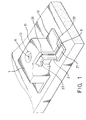
- an adhesive type LED lead frame includes a crystal base 1, a positive pole plate 2 and a joint 3, which is between the crystal base 1 and the positive pole plate.
- the crystal base 1 is a solid base as a negative pole and it is made of conductive material.
- the crystal base 1 at the center thereof has a seat part 11 with an elevation higher than rest part thereof and at two opposite sides thereof has a low adhesive part 12 respectively with a flat bottom and an elevation lower than the seat part 11.
- the adhesive part 12 can be adhered to a printed circuit board during the crystal base 1 being attached to the circuit board.
- the base part 11 is thicker than the melt part 12 to facilitate heat dissipation and there is a locating recess 13 at the top of the base part 11 for receiving a solid crystal or a chip A.
- the positive pole plate 2 is disposed at a lateral side of the crystal base 1 and also made of the same material as the crystal base 1.
- the positive pole 2 has a shape with a sense of direction corresponding to the crystal base 1 with a flat joining part 21 horizontally disposed for being adhered to the circuit board and a connecting part 22 extending upward and making a bend near the locating recess 13.
- the positive pole plate 2 is used as a positive pole while in use.
- the crystal base 1 can be integrally formed with the positive pole plate 2 by way of pressing, wax free casting, etching, powder metallurgy, die casting, extrusion forming, forging, stamping and etc.
- the base joint 3 is formed with a thinner thickness between the crystal base 1 and the base part 11. That is, the base joint 31 is between the connecting part 22 and the base part 11 and a flat joint 32 is between the adhesive part 12 and the flat joining part 21 so that an integral piece can be constituted before being worked.
- the base joint 31 is removed by way of such as being cut off after the solid crystal or chip A being placed in the locating recess and connected to a wire B and then it is packaged such that the base part 11 at the top thereof is joined to the top of the connecting part 22 to form a state of firmness as shown in Fig. 3.
- the flat joint 32 is removed to result in the positive plate 2 is separate from the crystal base 1 completely. In this way, it is not possible to occur the phenomenon of short circuit.
- Fig. 4 shows a perspective view after package.
- the lead frame of the present invention can be adhered to the circuit board to constitute a state of close circuit so that a trouble resulting from conventional pin insertion can be avoided.
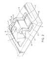
- the crystal base 1 at another lateral sides provides a second positive pole plate 4 at a side and a third positive pole plate 5 at another side so as to be opposite to each other with the locating recess 13 as a center thereof.
- the second and the third positive pole plates 4, 5 can be integrally formed with the crystal base 1 and have a thinner lower joint respectively. Then, the second and the third positive pole plates 4, 5 are removed sequentially before and after packaging. In this way, it is formed a configuration of three positive poles being disposed at both sides of the negative pole crystal base 1 so as to be used in case of two or more solid crystals or chips.
- the crystal base 1 at another lateral sides provides a second positive pole plate 4 at a side and a third positive pole plate 5 at another side so as to be opposite to each other with the locating recess 13 as a center thereof.
- the second and the third positive pole plates 4, 5 can be integrally formed with the crystal base 1 and have a thinner lower joint respectively.
- the second and the third positive pole plates 4, 5 are removed sequentially before and after packaging. In this way, it is formed a configuration of three positive poles being disposed at both sides of the negative pole crystal base 1 so as to be used in case of two or more solid crystals or chips.
- the first positive pole plate 2 is disposed at a lateral side of the crystal base 1 with the same material as the crystal base 1 and has a shape with a sense of direction corresponding to the crystal base 1.
- the first positive pole plate 2 has a horizontal flat joining part 21 adhered to the circuit board and a connecting part 22 extending upward and near the locating recess 13.
- the second positive pole plate 4 and the third positive pole plate 5 are disposed at another lateral side of the crystal base 1 and is made with the same material as the crystal base 1 with the shape and the sense thereof corresponding to the crystal base 1 so that a flat joining part 41, 51 is provided (not shown) respectively for being adhered to the circuit board with a connecting part 42, 52 extending upward near the locating recess 13 respectively.
- the first, second and third positive pole plates 2, 4, 5 have the same thickness as the crystal base 1 and are used as a positive pole respectively in practice.
- the base joint 3 is removed by way of such as being cut off after the solid crystal or chip A being placed in the locating recess and connected to a wire B and then it is packaged such that the positive plate 2 is separate from the crystal base 1 completely. In this way, it is not possible to occur the phenomenon of short circuit.
- Fig. 5 shows a perspective view after package.
- the adhesive type LED lead frame according to the present invention can be made with performing to prevent inconvenience from stamping bends done with conventional art and avoid defective products so as to provide an advantage of consistent quality and dimensions. Furthermore, it can enhance effects of conductivity and heat dissipation due to the crystal base 1 being solid so as to increase the stability of light emitting device.
Landscapes
- Led Device Packages (AREA)
- Structures For Mounting Electric Components On Printed Circuit Boards (AREA)
Abstract
Description
Claims (5)
- An adhesive type LED lead frame, comprising:a crystal base, being a conductive solid base, having a base part at a center thereof with a locating recess and having a lower thin adhesive part at two opposite sides thereof respectively;a positive pole plate, being disposed at a lateral side of the crystal base with a flat joining part parallel to the adhesive parts, having a connecting part with a sense of direction corresponding the base part; anda base joint and a flat joint, being disposed between the crystal base and the positive pole plate and provide a very thin thickness respectively;whereby, the base joint is removed before a solid crystal or a chip being placed in the base part with connecting wires thereof being packaged and the flat joint is removed after the packaging job so as to form two poles adhered to a circuit board.
- The adhesive type LED lead frame as defined in claim 1 is made with pressing, wax free casting, etching, powder metallurgy, die casting, extruded forming, forging, stamping or pre-casting.
- The adhesive type LED lead frame as defined in claim 1 is integrally made as a piece and made of copper, iron, aluminum or any other conductive metal.
- The adhesive type LED lead frame as defined in claim 1, wherein the crystal base at another lateral side thereof can provide a second positive pole plate and a third positive pole plate oppositely with each of the positive pole plates having a connecting part, a flat joining part and a joining part respectively.
- The adhesive type LED lead frame as defined in claim 4, wherein the first, the second and the third positive pole plates have a thickness thereof respectively being the same as the crystal base.
Applications Claiming Priority (2)
| Application Number | Priority Date | Filing Date | Title |
|---|---|---|---|
| CN03201554.2U CN2617039Y (en) | 2003-02-21 | 2003-02-21 | Adhesive LED lead frame |
| CN03201554 | 2003-02-21 |
Publications (2)
| Publication Number | Publication Date |
|---|---|
| EP1450413A2 true EP1450413A2 (en) | 2004-08-25 |
| EP1450413A3 EP1450413A3 (en) | 2009-08-05 |
Family
ID=32719976
Family Applications (1)
| Application Number | Title | Priority Date | Filing Date |
|---|---|---|---|
| EP03009573A Withdrawn EP1450413A3 (en) | 2003-02-21 | 2003-04-28 | Adhesive type LED lead frame |
Country Status (2)
| Country | Link |
|---|---|
| EP (1) | EP1450413A3 (en) |
| CN (1) | CN2617039Y (en) |
Families Citing this family (16)
| Publication number | Priority date | Publication date | Assignee | Title |
|---|---|---|---|---|
| US9070850B2 (en) | 2007-10-31 | 2015-06-30 | Cree, Inc. | Light emitting diode package and method for fabricating same |
| KR100631901B1 (en) * | 2005-01-31 | 2006-10-11 | 삼성전기주식회사 | LED package frame and LED package employing the same |
| US8669572B2 (en) | 2005-06-10 | 2014-03-11 | Cree, Inc. | Power lamp package |
| US7675145B2 (en) | 2006-03-28 | 2010-03-09 | Cree Hong Kong Limited | Apparatus, system and method for use in mounting electronic elements |
| US8748915B2 (en) | 2006-04-24 | 2014-06-10 | Cree Hong Kong Limited | Emitter package with angled or vertical LED |
| US7635915B2 (en) | 2006-04-26 | 2009-12-22 | Cree Hong Kong Limited | Apparatus and method for use in mounting electronic elements |
| US8735920B2 (en) | 2006-07-31 | 2014-05-27 | Cree, Inc. | Light emitting diode package with optical element |
| US8367945B2 (en) | 2006-08-16 | 2013-02-05 | Cree Huizhou Opto Limited | Apparatus, system and method for use in mounting electronic elements |
| US9711703B2 (en) | 2007-02-12 | 2017-07-18 | Cree Huizhou Opto Limited | Apparatus, system and method for use in mounting electronic elements |
| USD634863S1 (en) | 2008-01-10 | 2011-03-22 | Cree Hong Kong Limited | Light source of light emitting diode |
| US8791471B2 (en) | 2008-11-07 | 2014-07-29 | Cree Hong Kong Limited | Multi-chip light emitting diode modules |
| US8368112B2 (en) | 2009-01-14 | 2013-02-05 | Cree Huizhou Opto Limited | Aligned multiple emitter package |
| US9012938B2 (en) | 2010-04-09 | 2015-04-21 | Cree, Inc. | High reflective substrate of light emitting devices with improved light output |
| US8564004B2 (en) | 2011-11-29 | 2013-10-22 | Cree, Inc. | Complex primary optics with intermediate elements |
| US9601670B2 (en) | 2014-07-11 | 2017-03-21 | Cree, Inc. | Method to form primary optic with variable shapes and/or geometries without a substrate |
| US10622522B2 (en) | 2014-09-05 | 2020-04-14 | Theodore Lowes | LED packages with chips having insulated surfaces |
Family Cites Families (5)
| Publication number | Priority date | Publication date | Assignee | Title |
|---|---|---|---|---|
| JP3870301B2 (en) * | 1996-06-11 | 2007-01-17 | ヤマハ株式会社 | Semiconductor device assembly method, semiconductor device and continuous assembly system of semiconductor device |
| JP4215306B2 (en) * | 1998-08-27 | 2009-01-28 | シチズン電子株式会社 | Semiconductor package and manufacturing method thereof |
| US6667541B1 (en) * | 1998-10-21 | 2003-12-23 | Matsushita Electric Industrial Co., Ltd. | Terminal land frame and method for manufacturing the same |
| JP4102012B2 (en) * | 2000-09-21 | 2008-06-18 | 株式会社東芝 | Semiconductor device manufacturing method and semiconductor device |
| US20020163001A1 (en) * | 2001-05-04 | 2002-11-07 | Shaddock David Mulford | Surface mount light emitting device package and fabrication method |
-
2003
- 2003-02-21 CN CN03201554.2U patent/CN2617039Y/en not_active Expired - Fee Related
- 2003-04-28 EP EP03009573A patent/EP1450413A3/en not_active Withdrawn
Also Published As
| Publication number | Publication date |
|---|---|
| CN2617039Y (en) | 2004-05-19 |
| EP1450413A3 (en) | 2009-08-05 |
Similar Documents
| Publication | Publication Date | Title |
|---|---|---|
| US6957898B2 (en) | Adhesive type LED lead frame | |
| US8157415B2 (en) | Light emitting diode lighting module and method for making the same | |
| US6864567B2 (en) | Base of LED | |
| CN104916606B (en) | Semiconductor device and its manufacturing method | |
| CN102135244B (en) | Multiple light emitting diode light source lamps | |
| CN2617039Y (en) | Adhesive LED lead frame | |
| JP2003069083A (en) | Light emitting device | |
| US7888852B1 (en) | LED heat dissipation structure | |
| CN210516706U (en) | Packaging structure of a new type of power device | |
| US8697496B1 (en) | Method of manufacture integrated circuit package | |
| US20120314419A1 (en) | Heat dissipation structure of light-emitting diode | |
| CN101546711B (en) | Lead frame and manufacturing method thereof | |
| US20100006886A1 (en) | High power light emitting diode chip package carrier structure | |
| JP2003304000A (en) | Manufacturing method of light emitting diode package | |
| JP4760509B2 (en) | Lead frame assembly | |
| JP2006179541A (en) | Power LED lead frame and manufacturing method thereof | |
| JP2012222185A (en) | Lead frame, manufacturing method of the same and semiconductor device using lead frame | |
| JP6434269B2 (en) | Semiconductor device | |
| CN210156422U (en) | LED support and LED lamp pearl | |
| JP2013058574A (en) | Package for optical semiconductor device and optical semiconductor device | |
| US12622286B2 (en) | Side-wettable semiconductor package device with heat dissipation surface structure | |
| CN102447043B (en) | Light-emitting diode packaging structure | |
| JPH07106486A (en) | Lead frame, method of manufacturing the same, semiconductor device using the lead frame, and mounting substrate | |
| JP2008258530A (en) | Semiconductor light emitting device | |
| EP1557881A1 (en) | A lead-frame for electronic devices with extruded pads |
Legal Events
| Date | Code | Title | Description |
|---|---|---|---|
| PUAI | Public reference made under article 153(3) epc to a published international application that has entered the european phase |
Free format text: ORIGINAL CODE: 0009012 |
|
| AK | Designated contracting states |
Kind code of ref document: A2 Designated state(s): AT BE BG CH CY CZ DE DK EE ES FI FR GB GR HU IE IT LI LU MC NL PT RO SE SI SK TR |
|
| AX | Request for extension of the european patent |
Extension state: AL LT LV MK |
|
| RAP1 | Party data changed (applicant data changed or rights of an application transferred) |
Owner name: SUN RICH OPTO TECHNOLOGY CO., LTD. |
|
| RIN1 | Information on inventor provided before grant (corrected) |
Inventor name: SAN-HUA YU |
|
| PUAL | Search report despatched |
Free format text: ORIGINAL CODE: 0009013 |
|
| AK | Designated contracting states |
Kind code of ref document: A3 Designated state(s): AT BE BG CH CY CZ DE DK EE ES FI FR GB GR HU IE IT LI LU MC NL PT RO SE SI SK TR |
|
| AX | Request for extension of the european patent |
Extension state: AL LT LV MK |
|
| AKX | Designation fees paid | ||
| STAA | Information on the status of an ep patent application or granted ep patent |
Free format text: STATUS: THE APPLICATION IS DEEMED TO BE WITHDRAWN |
|
| 18D | Application deemed to be withdrawn |
Effective date: 20100206 |
|
| REG | Reference to a national code |
Ref country code: DE Ref legal event code: 8566 |