EP1447850A2 - Electronic parts packaging structure and method of manufacturing the same - Google Patents
Electronic parts packaging structure and method of manufacturing the same Download PDFInfo
- Publication number
- EP1447850A2 EP1447850A2 EP04250677A EP04250677A EP1447850A2 EP 1447850 A2 EP1447850 A2 EP 1447850A2 EP 04250677 A EP04250677 A EP 04250677A EP 04250677 A EP04250677 A EP 04250677A EP 1447850 A2 EP1447850 A2 EP 1447850A2
- Authority
- EP
- European Patent Office
- Prior art keywords
- electronic parts
- insulating film
- wiring pattern
- opening portion
- connection terminal
- Prior art date
- Legal status (The legal status is an assumption and is not a legal conclusion. Google has not performed a legal analysis and makes no representation as to the accuracy of the status listed.)
- Withdrawn
Links
Images







Classifications
-
- H—ELECTRICITY
- H10—SEMICONDUCTOR DEVICES; ELECTRIC SOLID-STATE DEVICES NOT OTHERWISE PROVIDED FOR
- H10W—GENERIC PACKAGES, INTERCONNECTIONS, CONNECTORS OR OTHER CONSTRUCTIONAL DETAILS OF DEVICES COVERED BY CLASS H10
- H10W70/00—Package substrates; Interposers; Redistribution layers [RDL]
- H10W70/60—Insulating or insulated package substrates; Interposers; Redistribution layers
- H10W70/611—Insulating or insulated package substrates; Interposers; Redistribution layers for connecting multiple chips together
-
- H—ELECTRICITY
- H10—SEMICONDUCTOR DEVICES; ELECTRIC SOLID-STATE DEVICES NOT OTHERWISE PROVIDED FOR
- H10W—GENERIC PACKAGES, INTERCONNECTIONS, CONNECTORS OR OTHER CONSTRUCTIONAL DETAILS OF DEVICES COVERED BY CLASS H10
- H10W70/00—Package substrates; Interposers; Redistribution layers [RDL]
- H10W70/60—Insulating or insulated package substrates; Interposers; Redistribution layers
-
- H—ELECTRICITY
- H05—ELECTRIC TECHNIQUES NOT OTHERWISE PROVIDED FOR
- H05K—PRINTED CIRCUITS; CASINGS OR CONSTRUCTIONAL DETAILS OF ELECTRIC APPARATUS; MANUFACTURE OF ASSEMBLAGES OF ELECTRICAL COMPONENTS
- H05K1/00—Printed circuits
- H05K1/18—Printed circuits structurally associated with non-printed electric components
- H05K1/182—Printed circuits structurally associated with non-printed electric components associated with components mounted in printed circuit boards [PCB], e.g. insert-mounted components [IMC]
- H05K1/185—Printed circuits structurally associated with non-printed electric components associated with components mounted in printed circuit boards [PCB], e.g. insert-mounted components [IMC] associated with components encapsulated in the insulating substrate of the PCBs; associated with components incorporated in internal layers of multilayer circuit boards
-
- H—ELECTRICITY
- H05—ELECTRIC TECHNIQUES NOT OTHERWISE PROVIDED FOR
- H05K—PRINTED CIRCUITS; CASINGS OR CONSTRUCTIONAL DETAILS OF ELECTRIC APPARATUS; MANUFACTURE OF ASSEMBLAGES OF ELECTRICAL COMPONENTS
- H05K1/00—Printed circuits
- H05K1/18—Printed circuits structurally associated with non-printed electric components
- H05K1/182—Printed circuits structurally associated with non-printed electric components associated with components mounted in printed circuit boards [PCB], e.g. insert-mounted components [IMC]
- H05K1/185—Printed circuits structurally associated with non-printed electric components associated with components mounted in printed circuit boards [PCB], e.g. insert-mounted components [IMC] associated with components encapsulated in the insulating substrate of the PCBs; associated with components incorporated in internal layers of multilayer circuit boards
- H05K1/186—Printed circuits structurally associated with non-printed electric components associated with components mounted in printed circuit boards [PCB], e.g. insert-mounted components [IMC] associated with components encapsulated in the insulating substrate of the PCBs; associated with components incorporated in internal layers of multilayer circuit boards manufactured by mounting on or connecting to patterned circuits before or during embedding
-
- H—ELECTRICITY
- H05—ELECTRIC TECHNIQUES NOT OTHERWISE PROVIDED FOR
- H05K—PRINTED CIRCUITS; CASINGS OR CONSTRUCTIONAL DETAILS OF ELECTRIC APPARATUS; MANUFACTURE OF ASSEMBLAGES OF ELECTRICAL COMPONENTS
- H05K3/00—Apparatus or processes for manufacturing printed circuits
- H05K3/30—Assembling printed circuits with electric components, e.g. with resistors
-
- H—ELECTRICITY
- H10—SEMICONDUCTOR DEVICES; ELECTRIC SOLID-STATE DEVICES NOT OTHERWISE PROVIDED FOR
- H10W—GENERIC PACKAGES, INTERCONNECTIONS, CONNECTORS OR OTHER CONSTRUCTIONAL DETAILS OF DEVICES COVERED BY CLASS H10
- H10W70/00—Package substrates; Interposers; Redistribution layers [RDL]
- H10W70/60—Insulating or insulated package substrates; Interposers; Redistribution layers
- H10W70/611—Insulating or insulated package substrates; Interposers; Redistribution layers for connecting multiple chips together
- H10W70/614—Insulating or insulated package substrates; Interposers; Redistribution layers for connecting multiple chips together the multiple chips being integrally enclosed
-
- H—ELECTRICITY
- H10—SEMICONDUCTOR DEVICES; ELECTRIC SOLID-STATE DEVICES NOT OTHERWISE PROVIDED FOR
- H10W—GENERIC PACKAGES, INTERCONNECTIONS, CONNECTORS OR OTHER CONSTRUCTIONAL DETAILS OF DEVICES COVERED BY CLASS H10
- H10W70/00—Package substrates; Interposers; Redistribution layers [RDL]
- H10W70/60—Insulating or insulated package substrates; Interposers; Redistribution layers
- H10W70/67—Insulating or insulated package substrates; Interposers; Redistribution layers characterised by their insulating layers or insulating parts
- H10W70/68—Shapes or dispositions thereof
- H10W70/685—Shapes or dispositions thereof comprising multiple insulating layers
-
- H—ELECTRICITY
- H10—SEMICONDUCTOR DEVICES; ELECTRIC SOLID-STATE DEVICES NOT OTHERWISE PROVIDED FOR
- H10W—GENERIC PACKAGES, INTERCONNECTIONS, CONNECTORS OR OTHER CONSTRUCTIONAL DETAILS OF DEVICES COVERED BY CLASS H10
- H10W72/00—Interconnections or connectors in packages
- H10W72/071—Connecting or disconnecting
-
- H—ELECTRICITY
- H10—SEMICONDUCTOR DEVICES; ELECTRIC SOLID-STATE DEVICES NOT OTHERWISE PROVIDED FOR
- H10W—GENERIC PACKAGES, INTERCONNECTIONS, CONNECTORS OR OTHER CONSTRUCTIONAL DETAILS OF DEVICES COVERED BY CLASS H10
- H10W90/00—Package configurations
-
- H—ELECTRICITY
- H05—ELECTRIC TECHNIQUES NOT OTHERWISE PROVIDED FOR
- H05K—PRINTED CIRCUITS; CASINGS OR CONSTRUCTIONAL DETAILS OF ELECTRIC APPARATUS; MANUFACTURE OF ASSEMBLAGES OF ELECTRICAL COMPONENTS
- H05K2201/00—Indexing scheme relating to printed circuits covered by H05K1/00
- H05K2201/01—Dielectrics
- H05K2201/0183—Dielectric layers
- H05K2201/0195—Dielectric or adhesive layers comprising a plurality of layers, e.g. in a multilayer structure
-
- H—ELECTRICITY
- H05—ELECTRIC TECHNIQUES NOT OTHERWISE PROVIDED FOR
- H05K—PRINTED CIRCUITS; CASINGS OR CONSTRUCTIONAL DETAILS OF ELECTRIC APPARATUS; MANUFACTURE OF ASSEMBLAGES OF ELECTRICAL COMPONENTS
- H05K2201/00—Indexing scheme relating to printed circuits covered by H05K1/00
- H05K2201/10—Details of components or other objects attached to or integrated in a printed circuit board
- H05K2201/10613—Details of electrical connections of non-printed components, e.g. special leads
- H05K2201/10621—Components characterised by their electrical contacts
- H05K2201/10636—Leadless chip, e.g. chip capacitor or resistor
-
- H—ELECTRICITY
- H05—ELECTRIC TECHNIQUES NOT OTHERWISE PROVIDED FOR
- H05K—PRINTED CIRCUITS; CASINGS OR CONSTRUCTIONAL DETAILS OF ELECTRIC APPARATUS; MANUFACTURE OF ASSEMBLAGES OF ELECTRICAL COMPONENTS
- H05K2201/00—Indexing scheme relating to printed circuits covered by H05K1/00
- H05K2201/10—Details of components or other objects attached to or integrated in a printed circuit board
- H05K2201/10613—Details of electrical connections of non-printed components, e.g. special leads
- H05K2201/10621—Components characterised by their electrical contacts
- H05K2201/10674—Flip chip
-
- H—ELECTRICITY
- H05—ELECTRIC TECHNIQUES NOT OTHERWISE PROVIDED FOR
- H05K—PRINTED CIRCUITS; CASINGS OR CONSTRUCTIONAL DETAILS OF ELECTRIC APPARATUS; MANUFACTURE OF ASSEMBLAGES OF ELECTRICAL COMPONENTS
- H05K3/00—Apparatus or processes for manufacturing printed circuits
- H05K3/46—Manufacturing multilayer circuits
- H05K3/4644—Manufacturing multilayer circuits by building the multilayer layer by layer, i.e. build-up multilayer circuits
-
- H—ELECTRICITY
- H10—SEMICONDUCTOR DEVICES; ELECTRIC SOLID-STATE DEVICES NOT OTHERWISE PROVIDED FOR
- H10W—GENERIC PACKAGES, INTERCONNECTIONS, CONNECTORS OR OTHER CONSTRUCTIONAL DETAILS OF DEVICES COVERED BY CLASS H10
- H10W20/00—Interconnections in chips, wafers or substrates
- H10W20/01—Manufacture or treatment
- H10W20/021—Manufacture or treatment of interconnections within wafers or substrates
- H10W20/023—Manufacture or treatment of interconnections within wafers or substrates the interconnections being through-semiconductor vias
-
- H—ELECTRICITY
- H10—SEMICONDUCTOR DEVICES; ELECTRIC SOLID-STATE DEVICES NOT OTHERWISE PROVIDED FOR
- H10W—GENERIC PACKAGES, INTERCONNECTIONS, CONNECTORS OR OTHER CONSTRUCTIONAL DETAILS OF DEVICES COVERED BY CLASS H10
- H10W70/00—Package substrates; Interposers; Redistribution layers [RDL]
- H10W70/01—Manufacture or treatment
- H10W70/05—Manufacture or treatment of insulating or insulated package substrates, or of interposers, or of redistribution layers
- H10W70/093—Connecting or disconnecting other interconnections thereto or therefrom, e.g. connecting bond wires or bumps
-
- H—ELECTRICITY
- H10—SEMICONDUCTOR DEVICES; ELECTRIC SOLID-STATE DEVICES NOT OTHERWISE PROVIDED FOR
- H10W—GENERIC PACKAGES, INTERCONNECTIONS, CONNECTORS OR OTHER CONSTRUCTIONAL DETAILS OF DEVICES COVERED BY CLASS H10
- H10W70/00—Package substrates; Interposers; Redistribution layers [RDL]
- H10W70/60—Insulating or insulated package substrates; Interposers; Redistribution layers
- H10W70/62—Insulating or insulated package substrates; Interposers; Redistribution layers characterised by their interconnections
- H10W70/65—Shapes or dispositions of interconnections
-
- H—ELECTRICITY
- H10—SEMICONDUCTOR DEVICES; ELECTRIC SOLID-STATE DEVICES NOT OTHERWISE PROVIDED FOR
- H10W—GENERIC PACKAGES, INTERCONNECTIONS, CONNECTORS OR OTHER CONSTRUCTIONAL DETAILS OF DEVICES COVERED BY CLASS H10
- H10W70/00—Package substrates; Interposers; Redistribution layers [RDL]
- H10W70/60—Insulating or insulated package substrates; Interposers; Redistribution layers
- H10W70/62—Insulating or insulated package substrates; Interposers; Redistribution layers characterised by their interconnections
- H10W70/65—Shapes or dispositions of interconnections
- H10W70/654—Top-view layouts
- H10W70/655—Fan-out layouts
-
- H—ELECTRICITY
- H10—SEMICONDUCTOR DEVICES; ELECTRIC SOLID-STATE DEVICES NOT OTHERWISE PROVIDED FOR
- H10W—GENERIC PACKAGES, INTERCONNECTIONS, CONNECTORS OR OTHER CONSTRUCTIONAL DETAILS OF DEVICES COVERED BY CLASS H10
- H10W72/00—Interconnections or connectors in packages
- H10W72/01—Manufacture or treatment
- H10W72/019—Manufacture or treatment of bond pads
-
- H—ELECTRICITY
- H10—SEMICONDUCTOR DEVICES; ELECTRIC SOLID-STATE DEVICES NOT OTHERWISE PROVIDED FOR
- H10W—GENERIC PACKAGES, INTERCONNECTIONS, CONNECTORS OR OTHER CONSTRUCTIONAL DETAILS OF DEVICES COVERED BY CLASS H10
- H10W72/00—Interconnections or connectors in packages
- H10W72/071—Connecting or disconnecting
- H10W72/072—Connecting or disconnecting of bump connectors
- H10W72/07231—Techniques
- H10W72/07232—Compression bonding, e.g. thermocompression bonding
- H10W72/07233—Ultrasonic bonding, e.g. thermosonic bonding
-
- H—ELECTRICITY
- H10—SEMICONDUCTOR DEVICES; ELECTRIC SOLID-STATE DEVICES NOT OTHERWISE PROVIDED FOR
- H10W—GENERIC PACKAGES, INTERCONNECTIONS, CONNECTORS OR OTHER CONSTRUCTIONAL DETAILS OF DEVICES COVERED BY CLASS H10
- H10W72/00—Interconnections or connectors in packages
- H10W72/071—Connecting or disconnecting
- H10W72/072—Connecting or disconnecting of bump connectors
- H10W72/07231—Techniques
- H10W72/07234—Using a reflow oven
-
- H—ELECTRICITY
- H10—SEMICONDUCTOR DEVICES; ELECTRIC SOLID-STATE DEVICES NOT OTHERWISE PROVIDED FOR
- H10W—GENERIC PACKAGES, INTERCONNECTIONS, CONNECTORS OR OTHER CONSTRUCTIONAL DETAILS OF DEVICES COVERED BY CLASS H10
- H10W72/00—Interconnections or connectors in packages
- H10W72/071—Connecting or disconnecting
- H10W72/072—Connecting or disconnecting of bump connectors
- H10W72/07231—Techniques
- H10W72/07236—Soldering or alloying
-
- H—ELECTRICITY
- H10—SEMICONDUCTOR DEVICES; ELECTRIC SOLID-STATE DEVICES NOT OTHERWISE PROVIDED FOR
- H10W—GENERIC PACKAGES, INTERCONNECTIONS, CONNECTORS OR OTHER CONSTRUCTIONAL DETAILS OF DEVICES COVERED BY CLASS H10
- H10W72/00—Interconnections or connectors in packages
- H10W72/071—Connecting or disconnecting
- H10W72/072—Connecting or disconnecting of bump connectors
- H10W72/07251—Connecting or disconnecting of bump connectors characterised by changes in properties of the bump connectors during connecting
-
- H—ELECTRICITY
- H10—SEMICONDUCTOR DEVICES; ELECTRIC SOLID-STATE DEVICES NOT OTHERWISE PROVIDED FOR
- H10W—GENERIC PACKAGES, INTERCONNECTIONS, CONNECTORS OR OTHER CONSTRUCTIONAL DETAILS OF DEVICES COVERED BY CLASS H10
- H10W72/00—Interconnections or connectors in packages
- H10W72/071—Connecting or disconnecting
- H10W72/072—Connecting or disconnecting of bump connectors
- H10W72/07251—Connecting or disconnecting of bump connectors characterised by changes in properties of the bump connectors during connecting
- H10W72/07254—Connecting or disconnecting of bump connectors characterised by changes in properties of the bump connectors during connecting changes in dispositions
-
- H—ELECTRICITY
- H10—SEMICONDUCTOR DEVICES; ELECTRIC SOLID-STATE DEVICES NOT OTHERWISE PROVIDED FOR
- H10W—GENERIC PACKAGES, INTERCONNECTIONS, CONNECTORS OR OTHER CONSTRUCTIONAL DETAILS OF DEVICES COVERED BY CLASS H10
- H10W72/00—Interconnections or connectors in packages
- H10W72/20—Bump connectors, e.g. solder bumps or copper pillars; Dummy bumps; Thermal bumps
-
- H—ELECTRICITY
- H10—SEMICONDUCTOR DEVICES; ELECTRIC SOLID-STATE DEVICES NOT OTHERWISE PROVIDED FOR
- H10W—GENERIC PACKAGES, INTERCONNECTIONS, CONNECTORS OR OTHER CONSTRUCTIONAL DETAILS OF DEVICES COVERED BY CLASS H10
- H10W72/00—Interconnections or connectors in packages
- H10W72/20—Bump connectors, e.g. solder bumps or copper pillars; Dummy bumps; Thermal bumps
- H10W72/241—Dispositions, e.g. layouts
-
- H—ELECTRICITY
- H10—SEMICONDUCTOR DEVICES; ELECTRIC SOLID-STATE DEVICES NOT OTHERWISE PROVIDED FOR
- H10W—GENERIC PACKAGES, INTERCONNECTIONS, CONNECTORS OR OTHER CONSTRUCTIONAL DETAILS OF DEVICES COVERED BY CLASS H10
- H10W72/00—Interconnections or connectors in packages
- H10W72/20—Bump connectors, e.g. solder bumps or copper pillars; Dummy bumps; Thermal bumps
- H10W72/241—Dispositions, e.g. layouts
- H10W72/247—Dispositions of multiple bumps
-
- H—ELECTRICITY
- H10—SEMICONDUCTOR DEVICES; ELECTRIC SOLID-STATE DEVICES NOT OTHERWISE PROVIDED FOR
- H10W—GENERIC PACKAGES, INTERCONNECTIONS, CONNECTORS OR OTHER CONSTRUCTIONAL DETAILS OF DEVICES COVERED BY CLASS H10
- H10W72/00—Interconnections or connectors in packages
- H10W72/20—Bump connectors, e.g. solder bumps or copper pillars; Dummy bumps; Thermal bumps
- H10W72/251—Materials
- H10W72/252—Materials comprising solid metals or solid metalloids, e.g. PbSn, Ag or Cu
-
- H—ELECTRICITY
- H10—SEMICONDUCTOR DEVICES; ELECTRIC SOLID-STATE DEVICES NOT OTHERWISE PROVIDED FOR
- H10W—GENERIC PACKAGES, INTERCONNECTIONS, CONNECTORS OR OTHER CONSTRUCTIONAL DETAILS OF DEVICES COVERED BY CLASS H10
- H10W72/00—Interconnections or connectors in packages
- H10W72/90—Bond pads, in general
-
- H—ELECTRICITY
- H10—SEMICONDUCTOR DEVICES; ELECTRIC SOLID-STATE DEVICES NOT OTHERWISE PROVIDED FOR
- H10W—GENERIC PACKAGES, INTERCONNECTIONS, CONNECTORS OR OTHER CONSTRUCTIONAL DETAILS OF DEVICES COVERED BY CLASS H10
- H10W72/00—Interconnections or connectors in packages
- H10W72/90—Bond pads, in general
- H10W72/921—Structures or relative sizes of bond pads
- H10W72/922—Bond pads being integral with underlying chip-level interconnections
-
- H—ELECTRICITY
- H10—SEMICONDUCTOR DEVICES; ELECTRIC SOLID-STATE DEVICES NOT OTHERWISE PROVIDED FOR
- H10W—GENERIC PACKAGES, INTERCONNECTIONS, CONNECTORS OR OTHER CONSTRUCTIONAL DETAILS OF DEVICES COVERED BY CLASS H10
- H10W72/00—Interconnections or connectors in packages
- H10W72/90—Bond pads, in general
- H10W72/921—Structures or relative sizes of bond pads
- H10W72/923—Bond pads having multiple stacked layers
-
- H—ELECTRICITY
- H10—SEMICONDUCTOR DEVICES; ELECTRIC SOLID-STATE DEVICES NOT OTHERWISE PROVIDED FOR
- H10W—GENERIC PACKAGES, INTERCONNECTIONS, CONNECTORS OR OTHER CONSTRUCTIONAL DETAILS OF DEVICES COVERED BY CLASS H10
- H10W72/00—Interconnections or connectors in packages
- H10W72/90—Bond pads, in general
- H10W72/941—Dispositions of bond pads
- H10W72/9413—Dispositions of bond pads on encapsulations
-
- H—ELECTRICITY
- H10—SEMICONDUCTOR DEVICES; ELECTRIC SOLID-STATE DEVICES NOT OTHERWISE PROVIDED FOR
- H10W—GENERIC PACKAGES, INTERCONNECTIONS, CONNECTORS OR OTHER CONSTRUCTIONAL DETAILS OF DEVICES COVERED BY CLASS H10
- H10W72/00—Interconnections or connectors in packages
- H10W72/90—Bond pads, in general
- H10W72/941—Dispositions of bond pads
- H10W72/9415—Dispositions of bond pads relative to the surface, e.g. recessed, protruding
-
- H—ELECTRICITY
- H10—SEMICONDUCTOR DEVICES; ELECTRIC SOLID-STATE DEVICES NOT OTHERWISE PROVIDED FOR
- H10W—GENERIC PACKAGES, INTERCONNECTIONS, CONNECTORS OR OTHER CONSTRUCTIONAL DETAILS OF DEVICES COVERED BY CLASS H10
- H10W74/00—Encapsulations, e.g. protective coatings
- H10W74/01—Manufacture or treatment
- H10W74/012—Manufacture or treatment of encapsulations on active surfaces of flip-chip devices, e.g. forming underfills
-
- H—ELECTRICITY
- H10—SEMICONDUCTOR DEVICES; ELECTRIC SOLID-STATE DEVICES NOT OTHERWISE PROVIDED FOR
- H10W—GENERIC PACKAGES, INTERCONNECTIONS, CONNECTORS OR OTHER CONSTRUCTIONAL DETAILS OF DEVICES COVERED BY CLASS H10
- H10W74/00—Encapsulations, e.g. protective coatings
- H10W74/10—Encapsulations, e.g. protective coatings characterised by their shape or disposition
- H10W74/15—Encapsulations, e.g. protective coatings characterised by their shape or disposition on active surfaces of flip-chip devices, e.g. underfills
-
- H—ELECTRICITY
- H10—SEMICONDUCTOR DEVICES; ELECTRIC SOLID-STATE DEVICES NOT OTHERWISE PROVIDED FOR
- H10W—GENERIC PACKAGES, INTERCONNECTIONS, CONNECTORS OR OTHER CONSTRUCTIONAL DETAILS OF DEVICES COVERED BY CLASS H10
- H10W90/00—Package configurations
- H10W90/20—Configurations of stacked chips
-
- H—ELECTRICITY
- H10—SEMICONDUCTOR DEVICES; ELECTRIC SOLID-STATE DEVICES NOT OTHERWISE PROVIDED FOR
- H10W—GENERIC PACKAGES, INTERCONNECTIONS, CONNECTORS OR OTHER CONSTRUCTIONAL DETAILS OF DEVICES COVERED BY CLASS H10
- H10W90/00—Package configurations
- H10W90/20—Configurations of stacked chips
- H10W90/22—Configurations of stacked chips the stacked chips being on both top and bottom sides of a package substrate, interposer or RDL
-
- H—ELECTRICITY
- H10—SEMICONDUCTOR DEVICES; ELECTRIC SOLID-STATE DEVICES NOT OTHERWISE PROVIDED FOR
- H10W—GENERIC PACKAGES, INTERCONNECTIONS, CONNECTORS OR OTHER CONSTRUCTIONAL DETAILS OF DEVICES COVERED BY CLASS H10
- H10W90/00—Package configurations
- H10W90/20—Configurations of stacked chips
- H10W90/297—Configurations of stacked chips characterised by the through-semiconductor vias [TSVs] in the stacked chips
-
- H—ELECTRICITY
- H10—SEMICONDUCTOR DEVICES; ELECTRIC SOLID-STATE DEVICES NOT OTHERWISE PROVIDED FOR
- H10W—GENERIC PACKAGES, INTERCONNECTIONS, CONNECTORS OR OTHER CONSTRUCTIONAL DETAILS OF DEVICES COVERED BY CLASS H10
- H10W90/00—Package configurations
- H10W90/701—Package configurations characterised by the relative positions of pads or connectors relative to package parts
- H10W90/721—Package configurations characterised by the relative positions of pads or connectors relative to package parts of bump connectors
- H10W90/722—Package configurations characterised by the relative positions of pads or connectors relative to package parts of bump connectors between stacked chips
-
- H—ELECTRICITY
- H10—SEMICONDUCTOR DEVICES; ELECTRIC SOLID-STATE DEVICES NOT OTHERWISE PROVIDED FOR
- H10W—GENERIC PACKAGES, INTERCONNECTIONS, CONNECTORS OR OTHER CONSTRUCTIONAL DETAILS OF DEVICES COVERED BY CLASS H10
- H10W90/00—Package configurations
- H10W90/701—Package configurations characterised by the relative positions of pads or connectors relative to package parts
- H10W90/721—Package configurations characterised by the relative positions of pads or connectors relative to package parts of bump connectors
- H10W90/724—Package configurations characterised by the relative positions of pads or connectors relative to package parts of bump connectors between a chip and a stacked insulating package substrate, interposer or RDL
-
- H—ELECTRICITY
- H10—SEMICONDUCTOR DEVICES; ELECTRIC SOLID-STATE DEVICES NOT OTHERWISE PROVIDED FOR
- H10W—GENERIC PACKAGES, INTERCONNECTIONS, CONNECTORS OR OTHER CONSTRUCTIONAL DETAILS OF DEVICES COVERED BY CLASS H10
- H10W90/00—Package configurations
- H10W90/701—Package configurations characterised by the relative positions of pads or connectors relative to package parts
- H10W90/731—Package configurations characterised by the relative positions of pads or connectors relative to package parts of die-attach connectors
- H10W90/734—Package configurations characterised by the relative positions of pads or connectors relative to package parts of die-attach connectors between a chip and a stacked insulating package substrate, interposer or RDL
-
- H—ELECTRICITY
- H10—SEMICONDUCTOR DEVICES; ELECTRIC SOLID-STATE DEVICES NOT OTHERWISE PROVIDED FOR
- H10W—GENERIC PACKAGES, INTERCONNECTIONS, CONNECTORS OR OTHER CONSTRUCTIONAL DETAILS OF DEVICES COVERED BY CLASS H10
- H10W99/00—Subject matter not provided for in other groups of this subclass
-
- Y—GENERAL TAGGING OF NEW TECHNOLOGICAL DEVELOPMENTS; GENERAL TAGGING OF CROSS-SECTIONAL TECHNOLOGIES SPANNING OVER SEVERAL SECTIONS OF THE IPC; TECHNICAL SUBJECTS COVERED BY FORMER USPC CROSS-REFERENCE ART COLLECTIONS [XRACs] AND DIGESTS
- Y02—TECHNOLOGIES OR APPLICATIONS FOR MITIGATION OR ADAPTATION AGAINST CLIMATE CHANGE
- Y02P—CLIMATE CHANGE MITIGATION TECHNOLOGIES IN THE PRODUCTION OR PROCESSING OF GOODS
- Y02P70/00—Climate change mitigation technologies in the production process for final industrial or consumer products
- Y02P70/50—Manufacturing or production processes characterised by the final manufactured product
Definitions
- the present invention relates to an electronic parts packaging structure and a method of manufacturing the same. More specifically, the present invention relates to an electronic parts packaging structure in which a semiconductor chip or the like is mounted on a wiring substrate in the state where the semiconductor chip or the like is buried in an insulating film, and to a method of manufacturing the same.
- Patent Literature 1 Japanese Unexamined Patent Publication No. 2001-177045
- Patent Literature 2 Japanese Unexamined Patent Publication No. 2000-323645 discloses a semiconductor device having a structure as follows: a plurality of semiconductor chips are three-dimensionally mounted on a wiring substrate in the state where the semiconductor chips are buried in insulating films, and the plurality of semiconductor chips are mutually connected using multilayered wiring patterns or the like formed with the insulating films interposed therebetween.
- Patent Literatures 1 and 2 there is no consideration for the fact that an interlayer insulating film is formed in the state where steps are generated due to the thickness of a semiconductor chip when the interlayer insulating film is formed on the mounted semiconductor chip.
- steps are also generated in the wiring patterns formed on the interlayer insulating film, reliability of bonding may be lowered when a semiconductor chip is flip-chip bonded to the wiring patterns.
- an electronic parts packaging structure having a structure in which an electronic parts is buried in an insulating film on a wiring substrate, wherein steps due to the thickness of the electronic parts may be eliminated to be planarized, and to provide a method of manufacturing the same.
- an electronic parts packaging structure including a wiring substrate having a wiring pattern, a first insulating film which is formed on the wiring substrate and which has an opening portion in a packaging area where an electronic parts is mounted, the electronic parts having a connection terminal flip-chip mounted on the wiring pattern of the opening portion of the first insulating film, a second insulating film for covering the electronic parts, a via hole formed in a predetermined portion of the first and second insulating films on the wiring pattern, and an upper wiring pattern formed on the second insulating film and connected to the wiring pattern through the via hole.
- the first insulating film (a resin film) having the opening portion in the packaging area is formed on the wiring substrate, and the connection terminal of the electronic parts (thinned semiconductor chip or the like) is flip-chip mounted on the wiring pattern in the opening portion.
- the second insulating film for covering the electronic parts is formed, and the via hole is formed in the first and second insulating films on the wiring pattern.
- the upper wiring pattern connected to the wiring pattern through the via hole is formed on the second insulating film.
- the first insulating film is formed so as to surround the electronic parts. Therefore, this embodiment of the present invention has a structure in which steps due to the thickness of the electronic parts are eliminated with the first insulating film. Accordingly, the second insulating film for covering the electronic parts is formed in the state where the upper surface of the second insulating film is planar, without being affected by the thickness of the electronic parts.
- the upper wiring pattern is stably formed with high precision.
- the electronic parts is flip-chip mounted on the wiring pattern in the state where the electronic parts is buried in a planar insulating film, and the upper wiring pattern for three-dimensionally multilayering a plurality of electronic parts is formed on the second insulating film without the occurrence of any trouble. Furthermore, in the case where an upper electronic parts is flip-chip mounted on the upper wiring pattern, a connection portion of the upper wiring pattern is placed at substantially the same height. Accordingly, the upper electronic parts is bonded thereto with high reliability.
- the second insulating film may be omitted by providing a protection film on the backside of the electronic parts.
- the upper wiring pattern is formed on the first insulating film and the protection film.
- the following structure may be adopted: without forming a via hole in the insulating film on the wiring pattern, a via hole penetrating the electronic parts is formed in a predetermined portion of the electronic parts on the connection terminal, and the upper wiring pattern is connected to the connection terminal through the via hole of the electronic parts.
- connection terminal of the electronic parts is made of gold
- a gold film is formed on a surface of the wiring pattern in the opening portion of the insulating film
- the connection terminal of the electronic parts is flip-chip mounted on the wiring pattern by gold-gold bonding.
- the first insulating film for eliminating steps due to the thickness of the electronic parts is also used as a mask layer for selectively forming the gold film on the wiring pattern (copper wiring or the like) in the opening portion (packaging area) of the first resin film. This makes it possible to easily flip-chip mount the electronic parts having the connection terminal made of gold on the wiring pattern by gold-gold bonding which provides high reliability of bonding.
- an electronic parts packaging structure including a wiring substrate having a wiring pattern, a first insulating film formed on the wiring substrate which has an opening portion in a packaging area where an electronic parts is mounted, the electronic parts mounted in the packaging area of the opening portion of the first insulating film in a state where a connection portion is directed upward, a second insulating film for covering the electronic parts, via holes respectively formed in predetermined portions of the insulating films on the connection terminal and the wiring pattern, and upper wiring patterns which are formed on the second insulating film and which are respectively connected to the connection terminal and the wiring pattern through the via holes.
- the first insulating film having the opening portion in the packaging area is formed on the wiring substrate, and the electronic parts is mounted in the opening portion in the state where the connection terminal is directed upward.
- the via holes are formed in predetermined portions in the second insulating film on the connection terminal and the' wiring pattern, respectively.
- the upper wiring patterns respectively connected to the connection terminal and the wiring pattern through the via holes are stably formed on the second insulating film with high precision.
- the second insulating film for covering the electronic parts may be omitted by use of an electronic parts provided with a passivation film having an opening portion for exposing the connection terminal, on the element formation surface.
- the upper wiring patterns are formed on the insulating film and the passivation film.
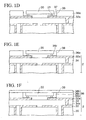
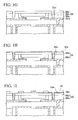
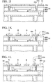
- FIGS. 1A to 1N are sectional views showing a method of manufacturing an electronic parts packaging structure of a first embodiment of the present invention in order.
- a base substrate 30 for manufacturing a build-up printed circuit board is prepared.
- the base substrate 30 is made of insulative material such as resin.
- Through-holes 30a are provided in the base substrate 30, and through-hole plating layers 30b connected to first wiring patterns 32 on the base substrate 30 are formed on the inner surfaces of the through-holes 30a. Openings of the through-holes 30a are filled with a resin body 30c.
- first interlayer insulating film 34 made of resin or the like, which covers the first wiring patterns 32 is formed. Then, predetermined portions of the first interlayer insulating film 34 on the first wiring patterns 32 are etched by a laser, RIE, or the like, thereby forming first via holes 34x having depths reaching the first wiring patterns 32.
- second wiring patterns 32a connected to the first wiring patterns 32 through the first via holes 34x are formed on the first interlayer insulating film 34.
- the second wiring patterns 32a are made of Cu wirings or the like and formed by a similar method to that of forming third wiring patterns to be described later.
- a wiring substrate 2, on which a semiconductor chip is mounted is obtained.
- first insulating film 36a epoxy series resin, polyimide series resin, novolac series resin, acrylic series resin, or the like is used.
- Methods of forming the first insulating film 36a include a method of patterning a photosensitive resin film by photolithography. Alternatively, a method may be employed in which a film-like resin layer is laminated to be formed or a resin film is formed by spin coating or printing, and then the resin film is etched by a laser or RIE, thereby forming the opening portion. Moreover, a method may be adopted in which a desired portion of a film-like resin layer is stamped out with a die to form the opening portion, and the resin film is attached. Furthermore, a resin film may be patterned into a shape having the opening portion by screen printing.
- Such a resin film is heat-treated at a temperature of 130 to 200 °C to be cured, thereby obtaining the first resin film 36a.
- One feature of the present embodiment is that when a structure in which a semiconductor chip is mounted in the state of being buried in an insulating film is formed, steps due to the thickness of the semiconductor chip are easily eliminated. Accordingly, in the present embodiment, the first insulating film 36a having the opening portion 39 in the packaging area A is formed to a thickness corresponding to the thickness of a semiconductor chip, and the semiconductor chip is mounted in the opening portion 39. Thus, steps due to the thickness of the semiconductor chip are easily eliminated with the first insulating film 36a.
- the thickness of the first insulating film 36a is appropriately adjusted in accordance with the thicknesses of various kinds of semiconductor chips.
- the thickness of the first insulating film 36a is set to a thickness equivalent to that of such a semiconductor chip.
- the opening portion 39 of the first insulating film 36a is preferably formed so as to surround a semiconductor chip to be mounted later.
- gold (Au) films 37 having thicknesses of 0.1 to 1 ⁇ m are selectively formed by electroless plating on the second wiring patterns (Cu wirings) 32a exposed in the opening portion 39 of the first insulating film 36a.
- the first insulating film 36a is made of a cured resin film, the first insulating film 36a is resistant to plating chemical for electroless plating.
- the Au films 37 may be formed after nickel (Ni) films have been formed as barrier films on the second wiring patterns (Cu wirings) 32a by electroless plating.
- the first insulating film 36a also functions as a mask layer for selectively forming the Au films 37 on connection portions B of the second wiring patterns (Cu wirings) 32a in the packaging area A.
- a semiconductor chip 20 having Au bumps 21 as shown in FIG. 1D is prepared.
- the semiconductor chip 20 is obtained as follows: a semiconductor wafer (not shown), which has elements, such as transistors, and connection pads on an element formation surface, is thinned to a thickness of approximately 150 ⁇ m (preferably, approximately 50 ⁇ m or less by grinding the backside of the semiconductor wafer, and then the semiconductor wafer is diced to be divided into individual pieces.
- the Au bumps 21 of the semiconductor chip 20 are formed on the connection pads before or after the semiconductor wafer is diced.
- connection pads and the bumps 21 of the semiconductor chip 20 are examples of connection terminals.
- the semiconductor chip 20 picked up with an ultrasonic tool is placed on the Au films 37 of the connection portions B of the second wiring patterns 32a in the state where the Au bumps 21 of the semiconductor chip 20 are directed downward, and ultrasonic vibration is applied horizontally while pressure is applied downward.
- the Au bumps 21 of the semiconductor chip 20 and the Au films 37 of the second wiring patterns 32a are bonded together.
- the semiconductor chip 20 is mounted on the second wiring patterns 32a by ultrasonic flip-chip bonding.
- the size of the opening portion 39 of the first insulating film 36a is preferably adjusted in accordance with the size of the semiconductor chip 20 so that a gap of 0.5 to 2 mm (preferably, approximately 1 mm) may be left between the side surfaces of the semiconductor chip 20 and those of the opening portion 39.
- the backside of the semiconductor chip 20 and the upper surface of the first insulating film 36a are at almost the same height, and steps due to the thickness of the semiconductor chip 20 are eliminated, because the first insulating film 36a is formed in an area except the packaging area A to almost the same thickness as that of the semiconductor chip 20 as previously described.
- the height of the backside of the semiconductor chip 20 and that of the upper surface of the first insulating film 36a may be different from each other to a degree in which troubles do not occur in subsequent steps.
- connection portions B of the second wiring patterns 32a can be bonded by Au-Au bonding at low cost.
- eliminating steps due to the thickness of the semiconductor chip 20 by forming the first insulating film 36a having the opening portion 39 in the packaging area A is very convenient for the case where the Au bumps 21 of the semiconductor chip 20 and the second wiring patterns 32a are bonded by Au-Au bonding, because the Au films 37 can be selectively formed on the connection portions B of the second wiring patterns 32a.
- Cu wirings having no Au films formed on the surfaces thereof is used as the second wiring patterns 32a,and the semiconductor chip 20 having solder bumps may be flip-chip bonded to the Cu wirings of the second wiring patterns 32a.
- the semiconductor chip 20 having solder bumps may be flip-chip bonded to the second wiring patterns 32a having the Au films 37 formed on the surfaces thereof as previously described.
- other various kinds of flip-chip mounting may be employed.
- a resin film having an opening portion in an area corresponding to the packaging area A may be attached after the semiconductor chip 20 is flip-chip mounted on the second wiring patterns 32a in the packaging area A.
- the opening portion of the resin film is stamped out with a die to be formed in advance.
- resin material is injected from the gap between the semiconductor chip 20 and the opening portion 39 of the first insulating film 36a, thereby filling the gap between the semiconductor chip 20 and the wiring substrate 2 and the gap between the semiconductor chip 20 and the side surfaces of the opening portion 39 of the first insulating film 36a with the resin material. Thereafter, the resin material is cured by heat treatment to become underfill resin 36c (filling insulating film).
- underfill resin 36c filling insulating film
- the underfill resin 36c may be formed as follows: insulating resin (NCF or NCP) is previously coated in a predetermined area including the packaging area A before the semiconductor chip 20 is flip-chip mounted, flip-chip bonding is performed in the state where this resin is interposed therebetween, and then the resin is cured by heat treatment to become the underfill resin 36c.
- insulating resin NCF or NCP
- the underfill resin 36c fills at least the gap between the under surface of the semiconductor chip 20 and the wiring substrate 2. This is because, even if concave portions remain in the gap between the side surfaces of the semiconductor chip 20 and those of the opening portion 39 of the first insulating film 36a, the concave portions are filled with a second insulating film, which is formed in the next step, to be planarized.
- the second insulating film 36b having a thickness of 5 to 20 ⁇ m, which covers the semiconductor chip 20, is formed.
- epoxy series resin, polyimide series resin, polyphenylene ether series resin, or the like is used for the second insulating film 36b.
- a method of forming the second insulating film 36b a method of laminating a resin film or a method of forming a resin film by spin coating or printing and then curing the resin film by heat treatment at a temperature of 130 to 200 °C is employed.
- the second insulating film 36b is formed on an underlying structure in which steps due to the thickness of the semiconductor chip 20 are eliminated. Accordingly, the second insulating film 36b is formed in the state where the upper surface thereof is planarized without being affected by the thickness of the semiconductor chip 20.
- a second interlayer insulating film 36 in a planarized state which is composed of the first insulating film 36a, the underfill resin 36c, and the second insulating film 36b, is obtained.
- a structure in which the semiconductor chip 20 is flip-chip mounted on the second wiring patterns 32a in the state where the semiconductor chip 20 is buried in the second interlayer insulating film 36 is formed.
- predetermined portions of the second interlayer insulating film 36 on the second wiring patterns 32a are etched by a YAG or CO 2 laser or RIE, thereby forming second via holes 36x having depths reaching the second wiring patterns 32a.
- a seed Cu film 32x is formed on the inner surfaces of the second via holes 36x and on the second interlayer insulating film 36 by electroless plating or sputtering.
- a resist film 33 having opening portions 33a corresponding to third wiring patterns to be formed later is formed on the seed Cu film 32 by photolithography.
- the second interlayer insulating film 36 is formed in a planarized state over all, defocus does not occur in photolithography. Therefore, a necessary pattern of the resist film 33 is stably formed with high precision.
- Cu film patterns 32y are formed in the second via holes 36x and the opening portions 33a of the resist film 33 by electroplating in which the seed Cu film 32x is utilized as a plating power-supply layer.
- the seed Cu film 32x is etched using the Cu film patterns 32y as a mask.
- third wiring patterns 32b (upper wiring patterns) which are composed of the seed Cu films 32x and the Cu film patterns 32y are formed on the second interlayer insulating film 36. These third wiring patterns 32b are connected to the second wiring patterns 32a through the second via holes 36x.
- the third wiring patterns 32b are formed in the condition demarcated with the pattern of the resist film 33 formed with high precision. Therefore, the third wiring pattern 32b required can be stably obtained.
- the second and third wiring patterns 32a and 32b may be formed through a subtractive process or a fully-additive process other than the aforementioned semi-additive process.
- a mode in which a plurality of semiconductor chips 20 are multilayered to be mutually connected in the state of being buried in respective interlayer insulating films may be formed by repeating the process from the step (FIG. 1B) of forming the first insulating film 36a having the opening portion 39 in the packaging area A of the wiring substrate 2 to the step (FIG. 1K) of forming the third wiring patterns 32b with a predetermined number of times.
- each interlayer insulating film is also formed in a planarized state. Accordingly, interlayer insulating films having semiconductor chips therein and wiring patterns can be formed in a stacking manner without the occurrence of any trouble.
- a mode in which semiconductor chips 20 are similarly buried in arbitrary interlayer insulating films among the plurality of interlayer insulating films may also be adopted.
- a mode in which a semiconductor chip 20 is also stacked on the backside of the base substrate 30 in the state where the semiconductor chip 20 is similarly buried in an interlayer insulating film may also be adopted.
- connection portions B to which bumps of an upper semiconductor chip are connected later, in the third wiring patterns 32b are drawn.
- solder resist film 38 having an opening portion 38a for exposing the connection portions B of the third wiring patterns 32b in a lump is formed.
- the solder resist film 38 is formed so as to surround a packaging area where the upper semiconductor chip is mounted later.
- connection portions B of the third wiring patterns 32b fine ones at a pitch of approximately 150 ⁇ m (e.g., line: 100 ⁇ m, space: 50 ⁇ m) or less are illustrated. Accordingly, if a continuous solder resist film having opening portions for exposing respective main parts of the connection portions B of the third wiring patterns 32b is formed, there are cases where the opening portions of the solder resist film are formed in the state of being shifted from the main parts of the connection portions B due to displacement in the forming process. If the opening portions of the solder resist film are placed in the state of being shifted from the main parts of the connection portions B, the bonding areas between the bumps of the upper semiconductor chip and the connection portions B are reduced. Therefore, bonding failures and the like are apt to occur with decrease in the bonding strength of the bumps.
- patterns of the solder resist film 38 are not formed in the packaging area where the connection portions B of the third wiring patterns 32b are placed, but the opening portion 38a is provided in the packaging area in a lump.
- the connection portions B of the third wiring patterns 32b troubles that the bonding area for flip-chip bonding becomes small do not occur.
- Ni films 40 and Au films 42 are selectively sequentially formed on the third wiring patterns 32b exposed in the opening portion 38a by electroless plating. Note that the Ni films 40 may be omitted in the case where barrier films are not required.
- the upper semiconductor chip 20x (upper electronic parts) having bumps 21 is prepared, and the bumps 21 of the upper semiconductor chip 20x are flip-chip bonded to the Au films 42 of the connection portions B of the third wiring patterns 32b.
- the bumps 21 of the upper semiconductor chip 20x Au bumps or solder bumps are used. In the case where Au bumps are used, Au-Au bonding is performed using ultrasonic waves. Meanwhile, in the case where solder bumps are used, bonding is performed by reflow heating.
- the solder resist film 38 does not exist in the packaging area where the connection portions B of the third wiring patterns 32b are placed. Accordingly, the bumps 21 of the upper semiconductor chip 20x are bonded to the connection portions B of the third wiring patterns 32b with high reliability in the state where necessary bonding areas can be obtained.
- the second interlayer insulating film 36 is formed in a planarized state over all, the respective connection portions B of the third wiring patterns 32b are placed at almost the same height. Therefore, the occurrence of bonding failures between the upper semiconductor chip 20x and the connection portions B of the third wiring patterns 32b is prevented.
- bumps are formed on the connection portions B of the third wiring patterns 32b by mounting solder bolls thereon, and connection terminals of the upper semiconductor chip 20x are bonded to these bumps.
- connection portions B of the third wiring patterns 32b are at a fine pitch of approximately 150 ⁇ m or less, the bumps 21 of the upper semiconductor chip 20x can be flip-chip bonded to the connection portions B of the third wiring patterns 32b with high reliability.
- the size of the opening portion 38a of the solder resist film 38 is appropriately adjusted in accordance with the size of the upper semiconductor chip 20x so that the dimensions from the peripheral portion of the upper semiconductor chip 20x to the side surfaces of the opening portion 38a of the solder resist film 38 may be 0.5 to 2 mm (preferably, approximately 1 mm).
- the gap between an element formation surface (under surface) of the upper semiconductor chip 20x and the third wiring patterns 32b and the gap between the element formation surface of the upper semiconductor chip 20x and the second interlayer insulating film 36 are filled with underfill resin 35.
- the underfill resin 35 is filled in the gap under the under surface of the upper semiconductor chip 20x and formed in the state of being blocked by the side surfaces of the opening portion 38a of the solder resist film 38.
- the above-described mode in which the solder resist film 38 is not formed in the packaging area where the respective connection portions B of the third wiring patterns 32b are placed is one preferred example when the upper semiconductor chip 20x having the bumps 21 at a fine pitch is flip-chip bonded. Therefore, a mode in which a solder resist film 38 having opening portions for the main parts of the respective connection portions B of the third wiring patterns 32b is continuously formed in the packaging area may be adopted.
- the first insulating film 36a having the opening portion 39 in the packaging area A of the wiring substrate 2 is formed.
- the semiconductor chip 20 is flip-chip mounted on the connection portions B of the second wiring patterns 32a in the opening portion 39 of the first insulating film 36a.
- the gap under the under surface of the semiconductor chip 20 and the gap adjacent to the side surfaces thereof are filled with the underfill resin 36c in an integrated state.
- the backside (upper surface) of the semiconductor chip 20, the upper surface of the first insulating film 36a, and the upper surface of the underfill resin 36c are adjusted to almost the same height, and planarized by eliminating steps due to the thickness of the semiconductor chip 20. Further, the second insulating film for covering the semiconductor chip 20 is formed in the state where the upper surface of the second insulating film is planarized.
- the semiconductor chip 20 is flip-chip mounted on the connection portions B of the second wiring patterns 32a in the state where the semiconductor chip 20 is buried in the planar second interlayer insulating film 36 composed of the first insulating film 36a, the second insulating film 36b, and the underfill resin 36c.
- the second via holes 36x are formed in predetermined portions of the second interlayer insulating film 36 on the second wiring patterns 32a, and the third wiring patterns 32b connected to the second wiring patterns 32a through the second via holes 36x are formed on the second interlayer insulating film 36.
- the bumps 21 of the upper semiconductor chip 20x are flip-chip bonded to the connection portions B of the third wiring patterns 32b. Furthermore, the gap under the under surface of the upper semiconductor chip 20x is filled with the underfill resin 35.
- the semiconductor chip 20 is flip-chip mounted in the opening portion 39 of the first insulating film 36a partly constituting the second interlayer insulating film.
- the semiconductor device 1 of the present embodiment has a structure in which steps due to the thickness of the semiconductor chip 20 are eliminated with the first insulating film 36a.
- the second insulating film 36b for covering the semiconductor chip 20 is formed in the state where the upper surface of the second insulating film 36b is planar, the third wiring patterns 32b formed on the second insulating film 36b are stably formed with high precision. Moreover, since the connection portions B of the third wiring patterns 32b are placed at almost the same height, reliability of bonding between the bumps 21 of the upper semiconductor chip 20x and the connection portions B of the third wiring patterns 32b can be improved.
- a packaging structure in which a plurality of semiconductor chips 20 are three-dimensionally multilayered to be mutually connected in the state of being buried in respective interlayer insulating films is easily manufactured without the occurrence of any trouble.
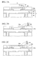
- FIGS. 2A to 2F are sectional views showing a method of manufacturing an electronic parts packaging structure of a second embodiment of the present invention in order.
- the second embodiment is different from the first embodiment in that a semiconductor chip having a protection film provided on the backside thereof is used and in that an insulating film for covering the semiconductor chip is not formed.
- similar steps to those of the first embodiment will not be further described in detail.
- a wiring substrate 2 similar to that of FIG. 1C in the first embodiment is prepared.
- a semiconductor chip 20a electronic parts
- the semiconductor chip 20a is one thinned to a thickness of approximately 150 ⁇ m (preferably, approximately 50 ⁇ m) or less.
- protection film 44 epoxy series resin, polyimide series resin, polyphenylene ether series resin, acrylic series resin, or the like is used.
- a method of forming the protection film 44 a method of laminating a resin film, a method of forming a resin film by spin coating or the dip method, or the like is employed.
- the protection film 44 may be formed after silane coupling agent is coated on the backside of the semiconductor chip 20a.
- the bumps 21 of the semiconductor chip 20a are flip-chip bonded to Au films 37 of second wiring patterns 32a exposed in an opening portion 39 (packaging area A) of a first insulating film 36a by a similar method to that of the first embodiment.
- the gap under the under surface of the semiconductor chip 20a and the gap adjacent to the side surfaces thereof are filled with underfill resin 36c (filling resin film).
- underfill resin 36c filling resin film
- a second insulating film does not need to be formed on the semiconductor chip 20a, unlike the first embodiment. Accordingly, in the present embodiment, a second interlayer insulating film 36 in which the semiconductor chip 20a is buried is composed of the insulating film 36a, the protection film 44, and the underfill resin 36c.
- predetermined portions of the second interlayer insulating film 36 on the second wiring patterns 32a are etched by a laser or RIE, thereby forming second via holes 36x having depths reaching the second wiring patterns 32a.
- third wiring patterns 32b (upper wiring patterns) connected to the second wiring patterns 32a through the second via holes 36x are formed on the second interlayer insulating film 36 by a similar method to that of the first embodiment.
- solder resist film 38 having an opening portion 38a for exposing respective connection portions B of the third wiring patterns 32b in a lump is formed on the structure of the FIG. 2D. Furthermore, Ni films 40 and Au films 42 are sequentially formed on the connection portions B of the third wiring patterns 32b by electroless plating.
- bumps 21 of an upper semiconductor chip 20x are flip-chip bonded to the Au films 42 of the connection portions B of the third wiring patterns 32b by a similar method to that of the first embodiment. Thereafter, similar to the first embodiment, the gap under the upper semiconductor chip 20x is filled with underfill resin 35.
- the manufacturing method is simplified compared to a method in which a second insulating film for covering the semiconductor chip is formed as in the first embodiment, and the cost of manufacture can be reduced.
- a semiconductor device can be made thinner than the first embodiment by use of the semiconductor chip 20a having the protection film 44 on the backside thereof.
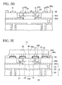
- FIGS. 3A to 3E are sectional views showing a method of manufacturing an electronic parts packaging structure of a third embodiment of the present invention in order.
- the third embodiment is different from the first and second embodiments in that, after a semiconductor chip is flip-chip mounted, via holes penetrating the semiconductor chip are formed therein, thus achieving mutual connection.
- similar steps to those of the first embodiment will not be further described in detail.
- a wiring substrate 2 having a similar structure to that of FIG. 1C in the first embodiment is prepared.
- a semiconductor chip 20b which has connection pads 23 and bumps 21 connected thereto on an element formation surface thereof and has a protection film 44 similar to that of the second embodiment on the backside thereof, is prepared.
- the connection pads 23 of the semiconductor chip 20b are obtained by rearranging electrode pads (not shown), which are arranged on the peripheral portion of the semiconductor chip 20b in a peripheral type arrangement, to an area array type arrangement by rewiring with Cu wirings.
- connection pads 23 and the bumps 21 connected thereto are examples of connection terminals.
- the gap under the under surface of the semiconductor chip 20b and the gap adjacent to the side surfaces thereof are filled with underfill resin 36c (filling insulating film) by a similar method to that of the first embodiment.
- underfill resin 36c filling insulating film
- a planarized second interlayer insulating film 36 composed of the insulating film 36a, the protection film 44 and the underfill resin 36c is obtained.
- second via holes 19 having depths reaching the connection pads 23 are formed by a laser or RIE in predetermined portions of the semiconductor chip 20b and the protection film 44 on the areas of the connection pads 23 except the areas to which the bumps 21 are bonded.
- the reason for forming the second via holes 19 on the connection pads in the areas except the areas to which the bumps 21 are bonded is that, if the second via holes 19 are formed above the areas to which the bumps 21 are bonded, damage can be caused at the joints between the connection pads 23 and the bumps 21 by a laser or RIE to lower reliability of bonding.
- third wiring patterns 32b (upper wiring patterns) connected to the connection pads 23 through the second via holes 19 formed in the semiconductor chip 20b are formed on the protection film 44 and the insulating film 36a through a semi-additive process, which has been described in the first embodiment, or the like.
- solder resist film 38 having an opening portion 38a for exposing connection portions B of the third wiring patterns 32b in a lump is formed.
- Ni films 40 and Au films 42 are sequentially formed on the respective connection portions B of the third wiring patterns 32b exposed in the opening portion 38a of the solder resist film 38 by a similar method to that of the first embodiment. Furthermore, after bumps 21 of an upper semiconductor chip 20x (upper electronic parts) having the bumps 21 are flip-chip bonded to the Au films 42 of the connection portions B of the third wiring patterns 32b, the gap under the under surface of the upper semiconductor chip 20x is filled with underfill resin 35.
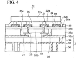
- FIG. 4 is a sectional view showing the electronic parts packaging structure according to the modified example of the third embodiment of the present invention.
- a semiconductor chip 20b having no protection film 44 on the backside thereof is used. Moreover, after the semiconductor chip 20b is flip-chip bonded to second wiring patterns 32a and underfill resin 36c is filled, a second insulating film 36b is formed on the semiconductor chip 20b similarly to the first embodiment.
- the second insulating film 36b for covering the semiconductor chip 20b and the semiconductor chip 20b are etched by a laser or RIE in the step of forming second via holes 19. Furthermore, third wiring patterns 32b are formed on the second insulating film 36b. Other components are the same as those of FIG. 3E and therefore will not be further described.
- the third embodiment has similar effects to those of the first embodiment.
- wiring length can be shortened. Therefore, it can respond to speeding up of a signal speed in semiconductor devices for high-frequency applications.
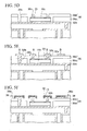
- FIGS. 5A to 5G are sectional views showing a method of manufacturing an electronic parts packaging structure of a fourth embodiment of the present invention in order.
- the fourth embodiment is different from the first to third embodiments in that a semiconductor chip is mounted face up.
- similar steps to those of the first embodiment will not be further described in detail.
- a wiring substrate 2 similar to that of FIG. 1C in the first embodiment is prepared. Thereafter, a first insulating film 36a having an opening portion 39 in a packaging area A is formed on the wiring substrate 2 by a similar method to that of the first embodiment.
- a semiconductor chip is mounted face up in the packaging area A (opening portion 39). Therefore, unlike the first to third embodiments, an Au film does not need to be formed in a portion of a second wiring pattern 32a in the packaging area A.
- the packaging area A of the wiring substrate 2 exposed in the opening portion 39 of the first insulating film 36a may be any one of a portion of the second wiring pattern 32a as shown in FIG. 5A, a portion of a first interlayer insulating film 34, and a portion in which the second wiring pattern 32a and the first interlayer insulating film 34 exist together.
- connection pads 23 connection terminals
- the semiconductor chip 20c is fixed on the second wiring pattern 32a exposed in the opening portion 39 of the first insulating film 36a, with an adhesive layer 46 interposed therebetween in the state where the connection pads 23 of the semiconductor chip 20c are directed upward (face up).
- the element formation surface of the semiconductor chip 20c and the upper surface of the first insulating film 36a come to be at almost the same height, thus eliminating steps due to the thickness of the semiconductor chip 20c.
- a second insulating film 36b is formed on the semiconductor chip 20c and the first insulating film 36a.
- the second insulating film 36b is formed using material and a method similar to those of the first embodiment.
- the second insulating film 36b is formed in the state where the upper surface thereof is planarized without being affected by steps due to the thickness of the semiconductor chip 20c. At this time, the gap between the side surfaces of the semiconductor chip 20c and those of the opening portion 39 of the first insulating film 36a is filled with the second insulating film 36b to be planarized.
- a second interlayer insulating film 36 composed of the first and second insulating films 36a and 36b is obtained, and a structure in which the semiconductor chip 20c is buried in the planar second interlayer insulating film 36 and mounted face up, is formed.
- predetermined portions of the second interlayer insulating film 36 on the connection pads 23 of the semiconductor chip 20c are etched by a laser or RIE, thereby forming second via holes 36x having depths reaching the connection pads 23.
- a predetermined portion of the second interlayer insulating film 36 on the second wiring pattern 32a is simultaneously etched, thereby simultaneously forming a second via hole 36x having a depth reaching the second wiring pattern 32a.
- third wiring patterns 32b (upper wiring patterns), respectively connected to the connection pads 23 of the semiconductor chip 20c and the second wiring pattern 32a through the second via holes 36x, are formed on the second interlayer insulating film 36 through a semi-additive process, which is described in the first embodiment.
- the process from the step (FIG. 5B) of mounting the semiconductor chip 20c face up in the opening portion 39 of the first insulating film 36a to the step (FIG. 5E) of forming the third wiring patterns 32b may be repeated with a predetermined number of times.
- a packaging structure in which a plurality of semiconductor chips 20c are buried face up in respective interlayer insulating films and mutually connected through via holes can be easily obtained without the occurrence of any trouble.
- a solder resist film 38 having an opening portion 38a for exposing respective connection portions B of the third wiring patterns 32b in a lump is formed.
- Ni films 40 and Au films 42 are sequentially formed on the third wiring patterns 32b exposed in the opening portion 38a of the solder resist film 38.
- an upper semiconductor chip 20x (upper electronic parts) having bumps 21 is prepared, and the bumps 21 of the upper semiconductor chip 20x are flip-chip bonded to the Au films 42 of the connection portions B of the third wiring patterns 32b. Then, similar to the first embodiment, the gap under the under surface of the upper semiconductor chip 20x is filled with underfill resin 35.
- the first insulating film 36a having the opening portion 39 in the packaging area A is formed on the wiring substrate 2. Moreover, the semiconductor chip 20c is mounted in the opening portion 39 of the first insulating film 36a in the state where the connection pads 23 of the semiconductor chip 20c are directed upward (face up). Thus, steps due to the thickness of the semiconductor chip 20c are eliminated with the first insulating film 36a.
- the second insulating film 36b for covering the semiconductor chip 20c is formed in the state where the upper surface of the second insulating film 36b is planarized, and the second interlayer insulating film 36 is composed of the first and second insulating films 36a and 36b.
- the semiconductor chip 20c is mounted face up in the state of being buried in the planar second interlayer insulating film 36.
- a second via holes 36x are formed in the second interlayer insulating film 36 on the connection pads 23 of the semiconductor chip 20c and the second wiring pattern 32a respectively.
- the third wiring patterns 32b connected to the connection pads 23 and the second wiring pattern 32a through the second via holes 36x, are formed on the second interlayer insulating film 36.
- the bumps 21 of the upper semiconductor chip 20x are flip-chip bonded to the connection portions B of the third wiring patterns 32b.
- FIG. 6 is a sectional view showing the electronic parts packaging structure according to the modified example of the fourth embodiment of the present invention.
- a second insulating film 36b is not formed on a semiconductor chip 20c.
- an insulating film which has high reliability of dielectric resistance, and which has opening portions 25a on connection pads 23, is used as a passivation film 25 of the semiconductor chip 20c.
- the material and thickness thereof are not particularly limited.
- the passivation film 25 is composed of a silicon nitride film having a thickness of approximately 0.5 ⁇ m and a polyimide resin film having a thickness of approximately 3 ⁇ m or more.
- a resin film having opening portions for exposing the connection pads 23 may be attached to the semiconductor chip 20c to become the passivation film 25.
- the gap between the side surfaces of the semiconductor chip 20c and those of the opening portion 39 of the first insulating film 36a is filled with underfill resin 36c to completely achieve planarization.
- the first insulating film 36a on a second wiring pattern 32a is etched, thereby forming a second via holes 36x.
- third wiring patterns 32b which are connected to the second wiring pattern 32a through the second via holes 36x and which are connected to the connection pads 23 through the opening portions 25a of the passivation film 25 are formed on the first insulating film 36a and the passivation film 25.
- a second insulating film 36b for covering the semiconductor chip 20c can be omitted.
- Other components are the same as those of FIG. 5G and therefore will not be further described.
- the semiconductor chip 20c is mounted face up in the opening portion 39 of the first insulating film 36a. Accordingly, similar to the case where a semiconductor chip is flip-chip mounted face down as in the first to third embodiments, steps due to the thickness of the semiconductor chip 20c are easily eliminated with the first insulating film 36a. Therefore, the fourth embodiment has similar effects to those of the first embodiment.
Landscapes
- Engineering & Computer Science (AREA)
- Microelectronics & Electronic Packaging (AREA)
- Manufacturing & Machinery (AREA)
- Production Of Multi-Layered Print Wiring Board (AREA)
- Encapsulation Of And Coatings For Semiconductor Or Solid State Devices (AREA)
- Wire Bonding (AREA)
- Structures Or Materials For Encapsulating Or Coating Semiconductor Devices Or Solid State Devices (AREA)
Abstract
Description
Claims (22)
- An electronic parts packaging structure comprising:a wiring substrate (2) having a wiring pattern (32a);a first insulating film (36a) formed on the wiring substrate (2), the first insulating film (36a) having an opening portion (39) in a packaging area (A) in which an electronic parts (20) is mounted;the electronic parts (20) having a connection terminal (21) flip-chip mounted on the wiring pattern (32a) exposed in the opening portion (39) of the first insulating film (36a);a second insulating film (36b) for covering the electronic parts (20);a via hole (36x) formed in a predetermined portion of the first and second insulating films (36a,36b) on the wiring pattern (32a); andan upper wiring pattern (32b) formed on the second insulating film (36b) and connected to the wiring pattern (32a) through the via hole (36x).
- An electronic parts packaging structure comprising:a wiring substrate (2) having a wiring pattern (32a);an insulating film (36a) formed on the wiring substrate (2), the insulating film (36a) having an opening portion (39) in a packaging area (A) in which an electronic parts (20a) is mounted;the electronic parts (20a) having a connection terminal (21) on an element formation surface thereof and having a protection film (44) on a backside thereof, the connection terminal (21) of the electronic parts (20a) being flip-chip mounted on the wiring pattern (32a) exposed in the opening portion (39) of the insulating film (36a);a via hole (36x) formed in a predetermined portion of the insulating film (36a) on the wiring pattern (32a); andan upper wiring pattern (32b) formed on the insulating film (36a) and the protection film (44), and connected to the wiring pattern (32a) through the via hole (36x).
- An electronic parts packaging structure comprising:a wiring substrate (2) having a wiring pattern (32a);an insulating film (36a) formed on the wiring substrate (2), the insulating film (36a) having an opening portion (39) in a packaging area (A) in which an electronic parts (20b) is mounted;the electronic parts (20b) having a connection terminal (21) on an element formation surface thereof and having a protection film (44) on a backside thereof, the connection terminal (21) of the electronic parts (20b) being flip-chip mounted on the wiring pattern (32a) exposed in the opening portion (39) of the insulating film (36a);a via hole (19) penetrating a predetermined portion of the electronic parts (20b) and the protection film (44) on the connection terminal (21, 23); andan upper wiring pattern (32b) formed on the insulating film (36a) and the protection film (44), and connected to the connection terminal (21) through the via hole (19) of the electronic parts (20b).
- An electronic parts packaging structure comprising:a wiring substrate (2) having a wiring pattern (32a);a first insulating film (36a) formed on the wiring substrate (2), the first insulating film (36a) having an opening portion (39) in a packaging area (A) in which an electronic parts (20b) is mounted;the electronic parts (20b) having a connection terminal (21) flip-chip mounted on the wiring pattern (32a) exposed in the opening portion (39) of the first insulating film (36a);a second insulating film (36b) for covering the electronic parts (20b);a via hole (19) penetrating a predetermined portion of the electronic parts (20b) and the second insulating film (36b) on the connection terminal (21, 23); andan upper wiring pattern (32b) formed on the second insulating film (36b) and connected to the connection terminal (21) through the via hole (19) of the electronic parts (20b).
- The electronic parts packaging structure according to any one of claims 1 to 4, wherein the connection terminal (21) of the electronic parts (20, 20a, 20b) is made of gold, a gold film is formed on a surface of the wiring pattern (32a) in the opening portion (39) of the insulating film (36a), and the connection terminal (21) of the electronic parts (20, 20a, 20b) is flip-chip mounted on the wiring pattern (32a) by gold-gold bonding.
- The electronic parts packaging structure according to any one of claims 1 to 5, wherein a structure in which the electronic parts (20, 20a, 20b) is flip-chip mounted in the opening portion (39) of the insulating film (37a) includes a structure in which a filling insulating film (36c) is formed in at least a gap between the electronic parts (20, 20a, 20b) and the wiring substrate (2) out of a gap between the electronic parts (20, 20a, 20b) and the wiring substrate (2) and a gap between the electronic parts (20, 20a, 20b) and side surfaces of the opening portion (39).
- An electronic parts packaging structure comprising:a wiring substrate (2) having a wiring pattern (32a);a first insulating film (36a) formed on the wiring substrate(2), the first insulating film (36a) having an opening portion (39) in a packaging area (A) in which an electronic parts (20c) is mounted;the electronic parts (20c) mounted in the packaging area (A) of the opening portion (39) of the first insulating film (36a) in a state where a connection terminal(23) is directed upward;a second insulating film (36b) for covering the electronic parts (20c);via holes (36x) respectively formed in predetermined portions of the insulating films (36a,36b) on the connection terminal (23) and the wiring pattern (32a); andupper wiring patterns (32b) formed on the second insulating film (36b), the upper wiring patterns (32b) being respectively connected to the connection terminal (23) and the wiring pattern (32a) through the via holes (36x).
- An electronic parts packaging structure comprising:a wiring substrate (2) having a wiring pattern (32a);an insulating film (36a) formed on the wiring substrate (2), the insulating film (36a) having an opening portion (39)in a packaging area (A) in which an electronic parts (20c) is mounted;the electronic parts (20c) which has a connection terminal (23) and a passivation film (25) having an opening portion (25a) for exposing the connection terminal (23) on an element formation surface thereof, and which is mounted in the packaging area (A) in the opening portion (39) of the insulating film (36a) in a state where the connection terminal (23) is directed upward;a via hole (36x) formed in a predetermined portion of the insulating film (36a) on the wiring pattern (2); andan upper wiring pattern (32b) formed on the insulating film (36a) and the passivation film (25), connected to the wiring pattern (32a) through the via hole (36x), and connected to the connection terminal (23) through the opening portion(25a).
- The electronic parts packaging structure according to any preceding claim, wherein an upper surface of the electronic parts (20 to 20c) and an upper surface of the insulating film (36a) having the opening portion (39) are adjusted to an almost same height.
- The electronic parts packaging structure according to any preceding claim, further comprising: an upper electronic parts (20x) having a connection terminal (21) flip-chip mounted on the upper wiring pattern (32b).
- The electronic parts packaging structure according to claim 10, wherein a solder resist film (38) having an opening portion (38a) opening a packaging area in which the upper electronic parts (20x) is mounted, in a lump, is formed on the insulating film (36a, 36b) and the upper wiring pattern (32b), and a filling insulating film (35) is formed in a gap under an under surface of the upper electronic parts (20x).
- The electronic parts packaging structure according to any preceding claim, wherein the electronic parts (20 to 20c) is a semiconductor chip having a thickness of approximately 150 µm or less, and the insulating film (36a, 36b) is made of resin.
- A method of manufacturing an electronic parts packaging structure, comprising the steps of:preparing a wiring substrate (2) having a wiring pattern (32a);forming a first insulating film (36a) having an opening portion (39) in a packaging area (A) in which an electronic parts (20) is mounted, on the wiring substrate (2);flip-chip mounting a connection terminal (21) of the electronic parts (20) on the wiring pattern (32a) exposed in the opening portion (39) of the first insulating film (36a);forming a second insulating film (36b) for covering the electronic parts;forming a via hole (36x) having a depth reaching the wiring pattern, in a predetermined portion of the first and second insulating films (36a, 36b) on the wiring pattern (32a); andforming an upper wiring pattern (32b) connected to the wiring pattern (32a) through the via hole (36x), on the second insulating film (36b).
- A method of manufacturing an electronic parts packaging structure, comprising the steps of:preparing a wiring substrate (2) having a wiring pattern (32a);forming an insulating film (36a) having an opening portion (39) in a packaging area (A) in which an electronic parts (20a) is mounted, on the wiring substrate (2);flip-chip mounting a connection terminal (21) of the electronic parts (20a) on the wiring pattern (32a) exposed in the opening portion (39) of the insulating film (36a), the electronic parts (20a) having the connection terminal (21) on an element formation surface thereof and having a protection film (44) on a backside thereof;forming a via hole (36x) having a depth reaching the wiring pattern (32a), in a predetermined portion of the insulating film (36a) on the wiring pattern; andforming an upper wiring pattern (32b) connected to the wiring pattern (32a) through the via hole (36x), on the insulating film (36a) and the protection film (44).
- A method of manufacturing an electronic parts packaging structure, comprising the steps of:preparing a wiring substrate (2) having a wiring pattern (32a);forming an insulating film (36a) having an opening portion (39) in a packaging area (A) in which an electronic parts (20b) is mounted, on the wiring substrate (2);flip-chip mounting a connection terminal (21) of the electronic parts (20b) on the wiring pattern (32a) exposed in the opening portion (39) of the insulating film (36a), the electronic parts (20b) having the connection terminal (21) on an element formation surface thereof and having a protection film (44) on a backside thereof;forming a via hole (19) having a depth reaching the connection terminal (21,23) by etching a predetermined portion of the electronic parts (20b) and the protection film (44) on the connection terminal (21,23); andforming an upper wiring pattern (32b) connected to the connection terminal (21) through the via hole (19), on the insulating film (36a) and the protection film (44).
- A method of manufacturing an electronic parts packaging structure, comprising the steps of:preparing a wiring substrate (2) having a wiring pattern (32a);forming a first insulating (36a) film having an opening portion (39) in a packaging area (A) in which an electronic parts (20b) is mounted, on the wiring substrate (2);flip-chip mounting a connection terminal (21) of the electronic parts (20b) on the wiring pattern (32a) exposed in the opening portion (39) of the first insulating film (36a);forming a second insulating film (36b) for covering the electronic parts (20b);forming a via hole (19) having a depth reaching the connection terminal (21, 23) by etching a predetermined portion of the electronic parts (20b) and the second insulating film (36b) on the connection terminal (21, 23); andforming an upper wiring pattern (32b) connected to the connection terminal (21) through the via hole (19), on the second insulating film (36b).
- The method according to any one of claims 13 to 16, after the step of forming the insulating film (36a) having the opening portion (39), and before the step of flip-chip mounting the electronic parts (20, 20a, 20b), further comprising the step of:wherein in the step of flip-chip mounting the electronic parts (20, 20a, 20b), the connection terminal (21) of the electronic parts (20, 20a, 20b), which is made of gold, is flip-chip mounted on the gold film (37) of the wiring pattern (32a).selectively forming a gold film (37) on the wiring pattern (32a) exposed in the opening portion (39) of the insulating film (36a) by electroless plating using the insulating film (36a) as a mask,
- The method according to any one of claims 13 to 17, wherein the step of flip-chip mounting the electronic parts (20, 20a, 20b)includes forming a filling insulating film (36c) between the electronic parts (20, 20a, 20b) and the wiring substrate (2).
- A method of manufacturing an electronic parts packaging structure, comprising the steps of:preparing a wiring substrate (2) having a wiring pattern (32a);forming a first insulating (36a) film having an opening portion (39) in a packaging area (A) in which an electronic parts (20c) is mounted, on the wiring substrate (2);mounting the electronic parts (20c) in the opening portion (39) of the first insulating film (36a) on the wiring substrate (2) in a state where a connection terminal (23) of the electronic parts (20c) is directed upward;forming a second insulating film (36b) for covering the electronic parts (20c);forming via holes (36x) in predetermined portions of the insulating films (36a, 36b) on the connection terminal (23) and the wiring pattern (32a), respectively; andforming upper wiring patterns (32b) respectively connected to the connection terminal (23) and the wiring pattern (32a) through the via holes (36x), on the second insulating film (36b).
- A method of manufacturing an electronic parts packaging structure, comprising the steps of:preparing a wiring substrate (2) having a wiring pattern (32a);forming an insulating film (36a) having an opening portion (39) in a packaging area (A) in which an electronic parts (20c)is mounted, on the wiring substrate (2);mounting the electronic parts (20c), which has a connection terminal (23) and a passivation film (25) having an opening portion (25a) for exposing the connection terminal (23) on an element formation surface thereof, in the opening portion (39) of the insulating film (36a) on the wiring substrate (2) in a state where the connection terminal (23) is directed upward;forming a via hole (36x) having a depth reaching the wiring pattern (32a) in a predetermined portion of the insulating film (36a) on the wiring pattern (32a); andforming an upper wiring pattern (32b) connected to the wiring pattern (32a) through the via hole (36x) and connected to the connection terminal (23) through the opening portion (25a), on the insulating film (36a) and the passivation film (25).
- The method according to any one of claims 13 to 20, wherein an upper surface of the electronic parts (20c) and an upper surface of the insulating film (36a) having the opening portion (39) are set to an almost same height.
- The method according to any one of claims 13 to 21, wherein the electronic parts (20c) is a semiconductor chip having a thickness of approximately 150 µm or less, and the insulating film (36a) is a resin film.
Applications Claiming Priority (2)
| Application Number | Priority Date | Filing Date | Title |
|---|---|---|---|
| JP2003035156 | 2003-02-13 | ||
| JP2003035156A JP4137659B2 (en) | 2003-02-13 | 2003-02-13 | Electronic component mounting structure and manufacturing method thereof |
Publications (2)
| Publication Number | Publication Date |
|---|---|
| EP1447850A2 true EP1447850A2 (en) | 2004-08-18 |
| EP1447850A3 EP1447850A3 (en) | 2010-07-21 |
Family
ID=32677606
Family Applications (1)
| Application Number | Title | Priority Date | Filing Date |
|---|---|---|---|
| EP04250677A Withdrawn EP1447850A3 (en) | 2003-02-13 | 2004-02-09 | Electronic parts packaging structure and method of manufacturing the same |
Country Status (6)
| Country | Link |
|---|---|
| US (4) | US7057290B2 (en) |
| EP (1) | EP1447850A3 (en) |
| JP (1) | JP4137659B2 (en) |
| KR (1) | KR101041011B1 (en) |
| CN (1) | CN1521847A (en) |
| TW (1) | TWI331389B (en) |
Cited By (3)
| Publication number | Priority date | Publication date | Assignee | Title |
|---|---|---|---|---|
| EP1761116A3 (en) * | 2005-08-26 | 2007-11-07 | Shinko Electric Industries Co., Ltd. | Circuit board having electronic parts mounted thereon by using under-fill material and method for producing the same |
| EP1656005A3 (en) * | 2004-11-08 | 2007-11-14 | Shinko Electric Industries Co., Ltd. | A substrate having a penetrating via and wiring connected to the penetrating via and a method for manufacturing the same |
| US8609539B2 (en) | 2005-11-02 | 2013-12-17 | Canon Kabushiki Kaisha | Embedded semiconductor device substrate and production method thereof |
Families Citing this family (67)
| Publication number | Priority date | Publication date | Assignee | Title |
|---|---|---|---|---|
| US7548430B1 (en) | 2002-05-01 | 2009-06-16 | Amkor Technology, Inc. | Buildup dielectric and metallization process and semiconductor package |
| US9691635B1 (en) | 2002-05-01 | 2017-06-27 | Amkor Technology, Inc. | Buildup dielectric layer having metallization pattern semiconductor package fabrication method |
| US20050056458A1 (en) * | 2003-07-02 | 2005-03-17 | Tsuyoshi Sugiura | Mounting pad, package, device, and method of fabricating the device |
| US20050270748A1 (en) * | 2003-12-16 | 2005-12-08 | Phoenix Precision Technology Corporation | Substrate structure integrated with passive components |
| US10811277B2 (en) | 2004-03-23 | 2020-10-20 | Amkor Technology, Inc. | Encapsulated semiconductor package |
| US11081370B2 (en) | 2004-03-23 | 2021-08-03 | Amkor Technology Singapore Holding Pte. Ltd. | Methods of manufacturing an encapsulated semiconductor device |
| JP2005317861A (en) * | 2004-04-30 | 2005-11-10 | Toshiba Corp | Semiconductor device and manufacturing method thereof |
| US20050258533A1 (en) * | 2004-05-21 | 2005-11-24 | Matsushita Electric Industrial Co., Ltd. | Semiconductor device mounting structure |
| US7179738B2 (en) * | 2004-06-17 | 2007-02-20 | Texas Instruments Incorporated | Semiconductor assembly having substrate with electroplated contact pads |
| KR100632257B1 (en) * | 2004-11-09 | 2006-10-11 | 삼성전자주식회사 | Wiring pattern structure of tap package for driving liquid crystal display |
| US7411303B2 (en) * | 2004-11-09 | 2008-08-12 | Texas Instruments Incorporated | Semiconductor assembly having substrate with electroplated contact pads |
| JP4800606B2 (en) * | 2004-11-19 | 2011-10-26 | Okiセミコンダクタ株式会社 | Method for manufacturing element-embedded substrate |
| TWI253714B (en) * | 2004-12-21 | 2006-04-21 | Phoenix Prec Technology Corp | Method for fabricating a multi-layer circuit board with fine pitch |
| JP4507101B2 (en) | 2005-06-30 | 2010-07-21 | エルピーダメモリ株式会社 | Semiconductor memory device and manufacturing method thereof |
| US20080023821A1 (en) * | 2005-07-20 | 2008-01-31 | Shih-Ping Hsu | Substrate structure integrated with passive components |
| US20080024998A1 (en) * | 2005-07-20 | 2008-01-31 | Shih-Ping Hsu | Substrate structure integrated with passive components |
| TWI297941B (en) * | 2005-10-13 | 2008-06-11 | Phoenix Prec Technology Corp | Semiconductor device with electroless plating metal connecting layer and method for fabricating the same |
| JP2007123524A (en) * | 2005-10-27 | 2007-05-17 | Shinko Electric Ind Co Ltd | Electronic component built-in board |
| US20070126085A1 (en) * | 2005-12-02 | 2007-06-07 | Nec Electronics Corporation | Semiconductor device and method of manufacturing the same |
| JP4668782B2 (en) * | 2005-12-16 | 2011-04-13 | 新光電気工業株式会社 | Mounting board manufacturing method |
| US7592202B2 (en) * | 2006-03-31 | 2009-09-22 | Intel Corporation | Embedding device in substrate cavity |
| JP2008010552A (en) * | 2006-06-28 | 2008-01-17 | Nec Electronics Corp | Power amplifier module |
| TWI304719B (en) * | 2006-10-25 | 2008-12-21 | Phoenix Prec Technology Corp | Circuit board structure having embedded compacitor and fabrication method thereof |
| JP5042591B2 (en) * | 2006-10-27 | 2012-10-03 | 新光電気工業株式会社 | Semiconductor package and stacked semiconductor package |
| DE102007022959B4 (en) * | 2007-05-16 | 2012-04-19 | Infineon Technologies Ag | Method for producing semiconductor devices |
| US7863088B2 (en) * | 2007-05-16 | 2011-01-04 | Infineon Technologies Ag | Semiconductor device including covering a semiconductor with a molding compound and forming a through hole in the molding compound |
| TWI348213B (en) * | 2007-08-15 | 2011-09-01 | Packaging substrate structure with capacitor embedded therein and method for fabricating the same | |
| KR100876899B1 (en) * | 2007-10-10 | 2009-01-07 | 주식회사 하이닉스반도체 | Semiconductor package |
| JP5353153B2 (en) * | 2007-11-09 | 2013-11-27 | パナソニック株式会社 | Mounting structure |
| US8093704B2 (en) * | 2008-06-03 | 2012-01-10 | Intel Corporation | Package on package using a bump-less build up layer (BBUL) package |
| US7851928B2 (en) * | 2008-06-10 | 2010-12-14 | Texas Instruments Incorporated | Semiconductor device having substrate with differentially plated copper and selective solder |
| US20100032194A1 (en) * | 2008-08-08 | 2010-02-11 | Ibiden Co., Ltd. | Printed wiring board, manufacturing method for printed wiring board and electronic device |
| WO2010101163A1 (en) * | 2009-03-04 | 2010-09-10 | 日本電気株式会社 | Substrate with built-in functional element, and electronic device using the substrate |
| US8247253B2 (en) | 2009-08-11 | 2012-08-21 | Pixart Imaging Inc. | MEMS package structure and method for fabricating the same |
| TWI396242B (en) | 2009-08-11 | 2013-05-11 | 原相科技股份有限公司 | Microelectronic device, manufacturing method of microelectronic device, microelectromechanical package structure and packaging method thereof |
| CN102001613B (en) * | 2009-09-02 | 2014-10-22 | 原相科技股份有限公司 | Microelectronic device and manufacturing method, microelectromechanical packaging structure and packaging method |
| JP5428667B2 (en) | 2009-09-07 | 2014-02-26 | 日立化成株式会社 | Manufacturing method of semiconductor chip mounting substrate |
| JP2011061004A (en) * | 2009-09-10 | 2011-03-24 | Elpida Memory Inc | Semiconductor device, and method of manufacturing the same |
| US8446017B2 (en) * | 2009-09-18 | 2013-05-21 | Amkor Technology Korea, Inc. | Stackable wafer level package and fabricating method thereof |
| US8796561B1 (en) * | 2009-10-05 | 2014-08-05 | Amkor Technology, Inc. | Fan out build up substrate stackable package and method |
| US8937381B1 (en) | 2009-12-03 | 2015-01-20 | Amkor Technology, Inc. | Thin stackable package and method |
| JP5136632B2 (en) * | 2010-01-08 | 2013-02-06 | 大日本印刷株式会社 | Electronic components |
| US20110215450A1 (en) * | 2010-03-05 | 2011-09-08 | Chi Heejo | Integrated circuit packaging system with encapsulation and method of manufacture thereof |
| JP5681374B2 (en) * | 2010-04-19 | 2015-03-04 | 日東電工株式会社 | Dicing tape integrated semiconductor backside film |
| JP5581830B2 (en) * | 2010-06-11 | 2014-09-03 | 富士通株式会社 | Manufacturing method of component-embedded substrate and component-embedded substrate |
| CN102275862B (en) * | 2010-06-11 | 2014-10-01 | 原相科技股份有限公司 | Micro-electromechanical packaging structure and manufacturing method thereof |
| US9337116B2 (en) * | 2010-10-28 | 2016-05-10 | Stats Chippac, Ltd. | Semiconductor device and method of forming stepped interposer for stacking and electrically connecting semiconductor die |
| US9391046B2 (en) * | 2011-05-20 | 2016-07-12 | STATS ChipPAC Pte. Ltd. | Semiconductor device and method of forming 3D semiconductor package with semiconductor die stacked over semiconductor wafer |
| JP6452270B2 (en) * | 2012-04-19 | 2019-01-16 | キヤノン株式会社 | Printed circuit boards and electronic equipment |
| CN104220954B (en) * | 2012-05-17 | 2018-07-17 | 英特尔公司 | Thin Film Insert Molding for Device Manufacturing |
| US8872349B2 (en) | 2012-09-11 | 2014-10-28 | Intel Corporation | Bridge interconnect with air gap in package assembly |
| EP2897166A4 (en) * | 2012-09-14 | 2016-06-29 | Renesas Electronics Corp | METHOD FOR MANUFACTURING SEMICONDUCTOR DEVICE |
| KR102042033B1 (en) * | 2012-10-30 | 2019-11-08 | 엘지이노텍 주식회사 | Printed circuit board for mounting chip and manufacturing method thereof |
| JP5682678B2 (en) * | 2013-08-28 | 2015-03-11 | 日立化成株式会社 | Semiconductor chip mounting substrate and manufacturing method thereof |
| TWI567886B (en) * | 2014-05-28 | 2017-01-21 | 南茂科技股份有限公司 | Chip package structure and chip package structure manufacturing method |
| CN105789161B (en) * | 2014-12-22 | 2019-07-12 | 恒劲科技股份有限公司 | Package structure and method for fabricating the same |
| US20160240457A1 (en) * | 2015-02-18 | 2016-08-18 | Altera Corporation | Integrated circuit packages with dual-sided stacking structure |
| KR102340053B1 (en) * | 2015-06-18 | 2021-12-16 | 삼성전기주식회사 | Printed circuit board and method of manufacturing the same |
| JP2017050313A (en) * | 2015-08-31 | 2017-03-09 | イビデン株式会社 | Printed wiring board and printed wiring board manufacturing method |
| JP2017050315A (en) * | 2015-08-31 | 2017-03-09 | イビデン株式会社 | Printed wiring board and printed wiring board manufacturing method |
| KR20170091436A (en) * | 2016-02-01 | 2017-08-09 | 삼성전자주식회사 | Image display apparatus and method for the same |
| JP2017156700A (en) * | 2016-03-04 | 2017-09-07 | 株式会社ジャパンディスプレイ | Display device |
| DE102018111389A1 (en) * | 2017-11-15 | 2019-05-16 | Taiwan Semiconductor Manufacturing Company, Ltd. | Semiconductor device and manufacturing method |
| CN110545635B (en) * | 2018-05-29 | 2021-09-14 | 鹏鼎控股(深圳)股份有限公司 | Method for manufacturing multilayer circuit board |
| KR102163059B1 (en) * | 2018-09-07 | 2020-10-08 | 삼성전기주식회사 | Printed circuit board with embedded interconnect structure |
| CN109300882A (en) * | 2018-09-20 | 2019-02-01 | 蔡亲佳 | Stacked embedded package structure and fabrication method thereof |
| JP7496251B2 (en) * | 2020-06-19 | 2024-06-06 | イビデン株式会社 | Component-embedded wiring board and method for manufacturing the component-embedded wiring board |
Family Cites Families (26)
| Publication number | Priority date | Publication date | Assignee | Title |
|---|---|---|---|---|
| US5367765A (en) * | 1990-08-31 | 1994-11-29 | Nec Corporation | Method of fabricating integrated circuit chip package |
| JPH04315458A (en) * | 1991-04-15 | 1992-11-06 | Sony Corp | Multilayered wiring board |
| JPH07123184B2 (en) * | 1991-12-17 | 1995-12-25 | 日本無線株式会社 | High-density mounting circuit board manufacturing method |
| US5353498A (en) * | 1993-02-08 | 1994-10-11 | General Electric Company | Method for fabricating an integrated circuit module |
| EP0635885B1 (en) * | 1993-07-22 | 1998-12-16 | Raytheon Company | High density circuit assembly |
| JPH08167630A (en) * | 1994-12-15 | 1996-06-25 | Hitachi Ltd | Chip connection structure |
| US5561085A (en) * | 1994-12-19 | 1996-10-01 | Martin Marietta Corporation | Structure for protecting air bridges on semiconductor chips from damage |
| JP2790122B2 (en) * | 1996-05-31 | 1998-08-27 | 日本電気株式会社 | Laminated circuit board |
| US6525414B2 (en) * | 1997-09-16 | 2003-02-25 | Matsushita Electric Industrial Co., Ltd. | Semiconductor device including a wiring board and semiconductor elements mounted thereon |
| KR100253363B1 (en) * | 1997-12-02 | 2000-04-15 | 김영환 | Semiconductor Package Substrate, Land Grid Array Semiconductor Package Using the Substrate and Method of Manufacturing The Same |
| JP2000332369A (en) * | 1999-05-25 | 2000-11-30 | Mitsui Mining & Smelting Co Ltd | Printed circuit board and manufacturing method thereof |
| JP3792445B2 (en) * | 1999-03-30 | 2006-07-05 | 日本特殊陶業株式会社 | Wiring board with capacitor |
| JP2000323645A (en) | 1999-05-11 | 2000-11-24 | Shinko Electric Ind Co Ltd | Semiconductor device and manufacturing method thereof |
| JP3670917B2 (en) * | 1999-12-16 | 2005-07-13 | 新光電気工業株式会社 | Semiconductor device and manufacturing method thereof |
| JP3494940B2 (en) * | 1999-12-20 | 2004-02-09 | シャープ株式会社 | Tape carrier type semiconductor device, manufacturing method thereof, and liquid crystal module using the same |
| WO2001063991A1 (en) * | 2000-02-25 | 2001-08-30 | Ibiden Co., Ltd. | Multilayer printed wiring board and method for producing multilayer printed wiring board |
| KR100668939B1 (en) | 2000-08-21 | 2007-01-12 | 앰코 테크놀로지 코리아 주식회사 | Board level semiconductor device and manufacturing method thereof |
| JP4447143B2 (en) * | 2000-10-11 | 2010-04-07 | 新光電気工業株式会社 | Semiconductor device and manufacturing method thereof |
| JP3420748B2 (en) * | 2000-12-14 | 2003-06-30 | 松下電器産業株式会社 | Semiconductor device and manufacturing method thereof |
| TW511405B (en) * | 2000-12-27 | 2002-11-21 | Matsushita Electric Industrial Co Ltd | Device built-in module and manufacturing method thereof |
| FR2819100B1 (en) * | 2000-12-28 | 2003-08-08 | Thomson Csf | METHOD FOR STACKING INTEGRATED CIRCUITS |
| TW511415B (en) * | 2001-01-19 | 2002-11-21 | Matsushita Electric Industrial Co Ltd | Component built-in module and its manufacturing method |
| JP4243922B2 (en) | 2001-06-26 | 2009-03-25 | イビデン株式会社 | Multilayer printed wiring board |
| US20030197285A1 (en) * | 2002-04-23 | 2003-10-23 | Kulicke & Soffa Investments, Inc. | High density substrate for the packaging of integrated circuits |
| KR100585677B1 (en) | 2004-07-02 | 2006-06-07 | 엘지전자 주식회사 | Message Handling Method in the LNPCP Library |
| US20090007996A1 (en) * | 2005-05-12 | 2009-01-08 | Battelle Memorial Institute | Method for Vibrating a Substrate During Material Formation |
-
2003
- 2003-02-13 JP JP2003035156A patent/JP4137659B2/en not_active Expired - Fee Related
-
2004
- 2004-01-30 KR KR1020040005988A patent/KR101041011B1/en not_active Expired - Fee Related
- 2004-02-05 US US10/771,506 patent/US7057290B2/en not_active Expired - Lifetime
- 2004-02-09 EP EP04250677A patent/EP1447850A3/en not_active Withdrawn
- 2004-02-09 TW TW093102945A patent/TWI331389B/en not_active IP Right Cessation
- 2004-02-13 CN CNA2004100049508A patent/CN1521847A/en active Pending
-
2006
- 2006-02-27 US US11/362,189 patent/US7545049B2/en not_active Expired - Lifetime
- 2006-09-22 US US11/524,933 patent/US7691673B2/en not_active Expired - Fee Related
-
2009
- 2009-04-21 US US12/385,814 patent/US7964950B2/en not_active Expired - Fee Related
Cited By (5)
| Publication number | Priority date | Publication date | Assignee | Title |
|---|---|---|---|---|
| EP1656005A3 (en) * | 2004-11-08 | 2007-11-14 | Shinko Electric Industries Co., Ltd. | A substrate having a penetrating via and wiring connected to the penetrating via and a method for manufacturing the same |
| US7365436B2 (en) | 2004-11-08 | 2008-04-29 | Shinko Electric Industries Co., Ltd. | Substrate having a penetrating via and wiring connected to the penetrating via and a method for manufacturing the same |
| EP1761116A3 (en) * | 2005-08-26 | 2007-11-07 | Shinko Electric Industries Co., Ltd. | Circuit board having electronic parts mounted thereon by using under-fill material and method for producing the same |
| US7663253B2 (en) | 2005-08-26 | 2010-02-16 | Shinko Electric Industries Co., Ltd. | Board having electronic parts mounted by using under-fill material and method for producing the same |
| US8609539B2 (en) | 2005-11-02 | 2013-12-17 | Canon Kabushiki Kaisha | Embedded semiconductor device substrate and production method thereof |
Also Published As
| Publication number | Publication date |
|---|---|
| US20040178510A1 (en) | 2004-09-16 |
| CN1521847A (en) | 2004-08-18 |
| TW200416997A (en) | 2004-09-01 |
| TWI331389B (en) | 2010-10-01 |
| US20090206471A1 (en) | 2009-08-20 |
| US7057290B2 (en) | 2006-06-06 |
| KR20040073301A (en) | 2004-08-19 |
| JP4137659B2 (en) | 2008-08-20 |
| US20070013048A1 (en) | 2007-01-18 |
| EP1447850A3 (en) | 2010-07-21 |
| US7691673B2 (en) | 2010-04-06 |
| US7545049B2 (en) | 2009-06-09 |
| US20060145359A1 (en) | 2006-07-06 |
| KR101041011B1 (en) | 2011-06-16 |
| JP2004247475A (en) | 2004-09-02 |
| US7964950B2 (en) | 2011-06-21 |
Similar Documents
| Publication | Publication Date | Title |
|---|---|---|
| US7057290B2 (en) | Electronic parts packaging structure and method of manufacturing the same | |
| US7573135B2 (en) | Electronic parts packaging structure in which a semiconductor chip is mounted on a wiring substrate and buried in an insulation film | |
| JP4251421B2 (en) | Manufacturing method of semiconductor device | |
| EP1427006B1 (en) | Electronic parts packaging structure and method of manufacturing the same | |
| US7563987B2 (en) | Electronic parts packaging structure and method of manufacturing the same | |
| JP3813402B2 (en) | Manufacturing method of semiconductor device | |
| US7723838B2 (en) | Package structure having semiconductor device embedded within wiring board | |
| US7791206B2 (en) | Semiconductor device and method of manufacturing the same | |
| JP4198566B2 (en) | Manufacturing method of electronic component built-in substrate | |
| JP2010135474A (en) | Multilayer wiring substrate and method for manufacturing same | |
| JP2001024089A (en) | System semiconductor device and method of manufacturing system semiconductor device | |
| CN119725297A (en) | Wiring substrate and method for manufacturing the same, and semiconductor device |
Legal Events
| Date | Code | Title | Description |
|---|---|---|---|
| PUAI | Public reference made under article 153(3) epc to a published international application that has entered the european phase |
Free format text: ORIGINAL CODE: 0009012 |
|
| AK | Designated contracting states |
Kind code of ref document: A2 Designated state(s): AT BE BG CH CY CZ DE DK EE ES FI FR GB GR HU IE IT LI LU MC NL PT RO SE SI SK TR |
|
| AX | Request for extension of the european patent |
Extension state: AL LT LV MK |
|
| PUAL | Search report despatched |
Free format text: ORIGINAL CODE: 0009013 |
|
| AK | Designated contracting states |
Kind code of ref document: A3 Designated state(s): AT BE BG CH CY CZ DE DK EE ES FI FR GB GR HU IE IT LI LU MC NL PT RO SE SI SK TR |
|
| AX | Request for extension of the european patent |
Extension state: AL LT LV MK |
|
| 17P | Request for examination filed |
Effective date: 20110117 |
|
| AKX | Designation fees paid |
Designated state(s): DE FR |
|
| 17Q | First examination report despatched |
Effective date: 20110628 |
|
| STAA | Information on the status of an ep patent application or granted ep patent |
Free format text: STATUS: THE APPLICATION IS DEEMED TO BE WITHDRAWN |
|
| 18D | Application deemed to be withdrawn |
Effective date: 20120110 |