EP1445575A1 - Verfahren und Anordnung zur Auswertung von Sendesignalen eines Tastsystems - Google Patents
Verfahren und Anordnung zur Auswertung von Sendesignalen eines Tastsystems Download PDFInfo
- Publication number
- EP1445575A1 EP1445575A1 EP03024230A EP03024230A EP1445575A1 EP 1445575 A1 EP1445575 A1 EP 1445575A1 EP 03024230 A EP03024230 A EP 03024230A EP 03024230 A EP03024230 A EP 03024230A EP 1445575 A1 EP1445575 A1 EP 1445575A1
- Authority
- EP
- European Patent Office
- Prior art keywords
- signals
- signal
- received signals
- differentiated
- received
- Prior art date
- Legal status (The legal status is an assumption and is not a legal conclusion. Google has not performed a legal analysis and makes no representation as to the accuracy of the status listed.)
- Granted
Links
Images




Classifications
-
- G—PHYSICS
- G01—MEASURING; TESTING
- G01B—MEASURING LENGTH, THICKNESS OR SIMILAR LINEAR DIMENSIONS; MEASURING ANGLES; MEASURING AREAS; MEASURING IRREGULARITIES OF SURFACES OR CONTOURS
- G01B21/00—Measuring arrangements or details thereof, where the measuring technique is not covered by the other groups of this subclass, unspecified or not relevant
- G01B21/02—Measuring arrangements or details thereof, where the measuring technique is not covered by the other groups of this subclass, unspecified or not relevant for measuring length, width, or thickness
- G01B21/04—Measuring arrangements or details thereof, where the measuring technique is not covered by the other groups of this subclass, unspecified or not relevant for measuring length, width, or thickness by measuring coordinates of points
- G01B21/047—Accessories, e.g. for positioning, for tool-setting, for measuring probes
-
- G—PHYSICS
- G01—MEASURING; TESTING
- G01B—MEASURING LENGTH, THICKNESS OR SIMILAR LINEAR DIMENSIONS; MEASURING ANGLES; MEASURING AREAS; MEASURING IRREGULARITIES OF SURFACES OR CONTOURS
- G01B5/00—Measuring arrangements characterised by the use of mechanical techniques
- G01B5/004—Measuring arrangements characterised by the use of mechanical techniques for measuring coordinates of points
- G01B5/008—Measuring arrangements characterised by the use of mechanical techniques for measuring coordinates of points using coordinate measuring machines
- G01B5/012—Contact-making feeler heads therefor
-
- G—PHYSICS
- G01—MEASURING; TESTING
- G01B—MEASURING LENGTH, THICKNESS OR SIMILAR LINEAR DIMENSIONS; MEASURING ANGLES; MEASURING AREAS; MEASURING IRREGULARITIES OF SURFACES OR CONTOURS
- G01B2210/00—Aspects not specifically covered by any group under G01B, e.g. of wheel alignment, caliper-like sensors
- G01B2210/58—Wireless transmission of information between a sensor or probe and a control or evaluation unit
Definitions
- the invention relates to a method for evaluating transmission signals Touch probe according to the preamble of claim 1 and an arrangement therefor according to the preamble of claim 24.
- a suitable detector arrangement is used and depending on the part signals generated by this detector arrangement, the touch probe emits its transmission signals ab, compare DE 101 32 554 A1.
- the corresponding switching signal is used as electromagnetic signal, in particular as an infrared signal, to a receiving unit transfer.
- the transmission signals of the touch probe are evaluated in order to Detect the occurrence of switching signals (i.e. a deflection of the probe element).
- the switching signal (and possibly other relevant transmission signals of the Touch probes, such as. B. a battery signal) of interference signals (caused z. B. by the To be able to distinguish between the infrared portion of dimmed neon tubes)
- the reception unit received signals (reception signals) with a reference signal compared and only further processed such signals, one by the reference signal exceed certain signal threshold.
- Such a method and an associated one Circuit arrangement are known from WO 99/41856 A1.
- the invention is based on the problem of a method and an arrangement of the to create the kind mentioned above, which is characterized by an improved distinction distinguish between transmit signals of the touch probe and interference signals.
- differentiating the received signals opens up the possibility of Differentiation of the transmission signals from interference signals based on the position of the edges of the Receive signals. This will be explained in more detail below.
- the transmission signals of the touch probe are preferably formed by substantially rectangular signal pulses, the Differentiate the received signals with the aim of determining the signal edges of the Signal pulses are performed and both the signal edges with a positive slope and the signal edges with a negative slope are subsequently evaluated.
- the transmission signals are through a sequence of signal packets is formed, each signal packet being a start signal and a Has stop signal and during each deflection of the probe element a switching signal occurs between its rest position between the start and the stop signal.
- start and stop signals By determining the timing of the rising and falling signal edges of the Start and stop signals that have predetermined, characteristic distances can the regular occurrence of start and stop signals are determined. This allows a reliable distinction between those limited by start and stop signals Signal packets of interference signals that have no comparable regularity.
- the switching signal By the switching signal to be emitted each time the probe element is deflected again at a defined position between a start and a stop signal is transmitted, the switching signals can be clearly based on the location identify their edges with respect to the start and stop signals. The same applies to Battery signals or other relevant transmission signals from the touch probe. this makes possible a further improved differentiation of evaluation-relevant transmission signals of the Touch probes from disturbing background signals.
- the electromagnetic transmission signals (infrared signals) of the touch probe and the Corresponding interference signals (i.e. the received signals) are assigned to the Receiver unit before differentiating by means of an optoelectronic element, for. B. in the form of a photodiode, converted into electrical signals (voltage signals), so that the signal processing and evaluation in the receiving unit based on the electrical signals.
- the reference signal which corresponds in particular to a reference voltage and which defines the signal thresholds on the basis of the transmission signals of the touch probe are identifiable, is preferably from the (converted into electrical signals) differentiated received signals formed by themselves from the differentiated Received signals generated useful signals are linked to the interference signals.
- the Useful signals are generated in such a way that they essentially only have the peak values of those portions of the differentiated received signals which are based on the Send signals go back.
- the link between the useful signals and the Interference signals to form a reference signal can in particular be caused by Averaging takes place, e.g. B. using an electrical voltage divider.
- Both the useful signals and the interference signals can be linked before they are linked each an effective value, e.g. B. corresponding to an envelope of the respective signal, are formed, in particular by using a capacitor circuit, the useful signals preferably by means of those used to form the effective value capacitor circuit used are generated from the received signals.
- a separation of the differentiated received signals into useful signals which are essentially the differentiated Transmit signals include, and in the comparatively low-frequency interference signals.
- An effective value of the useful signals (corresponding to the peaks the differentiated received signals) and the interference signals (corresponding to a Envelope of the interference signals) are formed.
- analog circuits electrical voltage dividers, Capacitor circuit
- Capacitor circuit can also be used to form the reference signal Circuit, in particular using a programmable logic module or a microprocessor can be used.
- a fast semiconductor memory in Form a shift register can be used, the received signal at a Evaluates multiple sampling points to determine the position of the edges of the relevant (the Transmit signal forming) signal pulses.
- the position of the sampling points is thereby defined by a periodic scanning signal, the frequency of which is many times greater is the signal rate of the pulses of the transmit signal. This can change the position of the flanks be determined with appropriate accuracy.
- a programmable one can also be used Logic device or a microprocessor can be used in the context of a digital Circuit to determine the edges of the received signal.
- the regular Occurrence of start and stop signals based on the characteristic location of their Signal edges are identifiable to each other on the readiness of the touch probe be closed if this regularly corresponds in standby mode Sends out signal packets. If, in addition, with each deflection of the probe generated switching signals each at a defined distance between a start and a Stop signal are sent, then these signals are based on the characteristic position of their edges reliably within a signal packet identifiable. The same applies to any battery signals to be sent with which For example, the need to point out the battery of the touch probe renew.
- a particular reliability of the method is achieved if after the Differentiate the received signals with positive and negative signal edges Slope can be processed and evaluated in a separate circuit.
- An arrangement for evaluating the transmission signals of a touch probe in particular is suitable for performing the method according to the invention is by the Features of claim 24 characterized.
- a touch probe T is shown, which is used to determine the position and contour one clamped in a machine tool, for example a milling machine Serves workpiece and includes a probe for this.
- the probe is by means of a Cone K can be inserted into a spindle of the corresponding machine tool.
- the touch probe T has at its end opposite the cone K.
- Probe element E in the form of a stylus with a probe ball A, which in all Directions is movably mounted on the housing of the touch probe.
- the rest position of the Probe element E is usually on the axis of symmetry of the probe system T, as in Figure 1 shown.
- the touch probe has one assigned to the touch element E.
- Detector arrangement D with which a deflection of the probe element E, for example by an optical transmitter (in the form of an LED) and an associated sensor (in Shape of a differential photo element) is detectable.
- an optical transmitter in the form of an LED
- an associated sensor in Shape of a differential photo element
- the of the detector arrangement D depending on the deflection of the Output voltage probe element E is amplified and a trigger T1 fed.
- the trigger T1 contains a reference voltage as a further input signal, which is made available, for example, by a programmable logic module L. becomes.
- the reference voltage defines the switching threshold above which the Output voltage of the amplifier downstream of the detector arrangement D as Reference to a deflection of the sensing element E applies.
- the Logic module L via a dedicated IR transmitter S from the touch probe a corresponding infrared signal (switching signal) to an assigned receive and Evaluation unit I / O sent, compare Figure 1.
- the logic module L des Trigger T2 assigned to the touch probe is used to monitor the battery voltage and ensures the delivery of a battery signal to the assigned receive and Evaluation unit I / O if a battery change is required in the touch probe.
- Figure 1 shows different possible arrangements of the reception and Evaluation unit I / O with respect to the probe of the touch probe T, in particular regarding its IR transmitter S.
- the possible radiation angle of the by evenly on Scope of the housing of the touch system T arranged LEDs formed transmitter S according to FIG. 1 are either 0 °, + 30 ° or -30 °.
- the touch probe T when it is ready for operation data packets 100 are sent to the server at regular intervals of approximately 3 ms assigned receiving unit sent. These are formed by IR radiation
- data packets consist of a plurality of rectangular ones Signal pulses, namely a start bit 101 and a stop bit 105, between which still a switching signal 102 and a battery signal 104 can be arranged.
- Words are expressed regularly when the touch probe is ready Data packets 100 are sent, each having a start bit 101 and a stop bit 105 have, wherein between the end of the start bit 101 and the beginning of the respective Stop bit 105 is a defined period of 16 microseconds.
- a deflection of the probe element is detected, so occurs between the start bit 101 and the stop bit 105 at a defined time interval from the falling edge of the Start bit (3.2 microseconds) on a switching signal 102.
- a battery signal 104 can be provided to a indicate the need to change the touch probe battery.
- the receiving unit assigned to the touch probe comprises as a receiver a photodiode 1 with a downstream amplifier 10 and one of the photodiode 1 downstream differentiating element 2 with a further downstream amplifier 20.
- the differentiating element 2 and amplifier 20 are two identical Subsequent evaluation circuits 3, 3 ', the second evaluation circuit 3' an inverter 25 is connected upstream.
- Each of the two evaluation circuits 3, 3 serves in each case to compare the means of the Differentiator 2 differentiated signal with a reference signal in a trigger 4 and for the evaluation of such signals that one by the reference signal (in the form of a Reference voltage) exceed the defined threshold value in a shift register 5.
- a reference voltage based on the output voltage of the Differentiator 2 with a downstream amplifier 20 has each of the two circuits 3, 3 'in a first branch an electrical component 30, e.g. in the form of a diode, which is only permeable to electrical signals if the input voltage is greater than that on the output side at a downstream capacitor 31 falling voltage, which in turn can discharge through a resistor 32.
- the electrical components of the capacitor circuit 30, 31, 32 are especially with regard to the decay time of the capacitor, for example 15 ms can be chosen so that the capacitor circuit 30, 31, 32 its maximum Effectiveness achieved on signals of high frequency (leading to a subordinate Amplifier 33 can be passed). This is mainly about the Transmit signals from the probe.
- the levels of these differentiated transmission signals are in the Usually significantly higher than the level of the differentiated interference signals.
- the respective evaluation circuit 3, 3 has another electrical component 35 (in the form of a diode), which is only then for electrical Signals is permeable if the input voltage is greater than that output-side voltage drop across a downstream capacitor 36, the can in turn discharge through a resistor 37. Between that electrical Component 35 and the capacitor 36 connected downstream of the component 35 is a electrical resistor 35a switched. This resistor 35a is selected so that the Capacitor 36 (decay time e.g. 21 ms) is not due to those generated by the touch probe Data packets 100 (compare FIGS.
- the capacitor 36 upstream electrical resistance 35a causes a delay in the Response time of the evaluation circuit, so that the very short signal packets 100 by sent to the touch probe, no significant charging of the effect corresponding capacitor 36.
- the capacitor is therefore in Essentially only charged by the comparatively low-frequency interference signals, which are formed, for example, by the infrared portion of fluorescent tubes.
- the two capacitor circuits 30, 31, 32 and 35, 35a, 36, 37 a separation of the differentiated received signals into useful signals that in essentially include the differentiated transmission signals, and in the comparatively low-frequency interference signals.
- an effective value of the Useful signals (corresponding to the peaks of the differentiated received signals) and the Interference signals (corresponding to an envelope of the interference signals) are formed as follows will be explained in more detail.
- the two capacitor circuits 30, 31, 32 and 35, 35a, 36, 37 of the respective Evaluation circuit 3, 3 ' is followed by an amplifier 33 and 38, respectively the former amplifier the gain factor one and the second amplifier has a gain factor greater than one.
- the two branches of the respective evaluation circuit 3, 3 ' connected to a voltage divider 39, which is formed by two resistors.
- the voltage tapped by this voltage divider is the one input of the supplied to respective triggers 4, at the other input of which the output signal the differentiator 2.
- the trigger 4 of the respective evaluation circuit 3, 3 ' is a Shift register 5 connected downstream.
- the IR signals of the touch probe and the infrared interference signals that are also present together form the receive signals of the receive unit I / O, an electrical one Signal, namely a voltage signal, which is then in the Differentiator 2 is differentiated.
- This will cause low frequency interference eliminated the z. B. can come from fluorescent tubes.
- Rising edges cause a positive voltage pulse and falling ones Edges of the transmission signal a negative voltage pulse of the differentiated Signal.
- the positive and negative voltage pulses 3, 3 ' are in the two evaluation circuits 3, 3 'arranged downstream of the differentiator 2, the falling edges or the corresponding voltage pulses of the differentiated signals of the evaluation circuit 3 'with the upstream inventor 25 assigned.
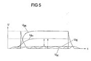
- FIG. 5 shows how, by averaging the peak values U pk of the differentiated received signal with an effective value (envelope U E ) of the interference signals U st, an effective voltage value U tn is formed which, as a reference voltage, the trigger threshold of the trigger 4 of the respective evaluation circuit 3, 3 ' Are defined. 5 shows the differentiated signals corresponding to the rising edge of a start bit and the rising edge of a stop bit.
- the trigger 4 of the respective evaluation circuit 3, 3 'recognizes those signals as transmission signals whose amplitude exceeds the trigger threshold defined by the reference voltage U tn . Because the reference voltage U tn is formed by linking the peak values of the differentiated received signals with an envelope of the interference signals, the trigger threshold rises with increasing amplitude of the interference signals. As a result, the risk of false triggers of the respective trigger 4 due to interference signals is largely eliminated. Because the trigger threshold is above the envelope of the interference signals.
- the trigger threshold by linking (averaging) the peak values of the received signals with the Zero potential formed, the trigger threshold would be independent of the interference signals and there would be an increased risk of interference signals triggering the trigger 4 incorrectly to lead.
- the trigger threshold By linking the peak values of the (differentiated) received signals with an effective value of the interference signals for formation the trigger threshold can in particular be the interference effects of high-frequency interference signals be eliminated. This complements the elimination of low-frequency interference signals by the Differentiating the received signals described above before further processing them and evaluation.
- Figure 6a shows schematically once again the two shift registers 5 from Figure 4, each downstream of a trigger 4 and with a (not shown in detail) Evaluation logic are linked.
- Figure 6b shows schematically the positive (top) and negative (bottom) Voltage pulses of a differentiated data packet, which result from the transmission signals of the touch probe was won. After differentiating, the increasing ones and falling edges of the data packet by positive or negative Voltage pulses represent, as shown in Figure 4a.
- data are read in at seventy-two sampling points, see FIG. 6b.
- the time interval (0.4 microseconds) between two successive read-in processes into the shift register is therefore a seventy-second of the duration of a signal packet 100. This results in a correspondingly high accuracy in the evaluation of the data packets.
- the one shift register 5 is used for Determination of the position of the rising edges and the other shift register 5 for Determining the position of the falling edges of the data packets. These are in the differentiated output signal by positive or negative signal pulses represents.
- edges of a possible switching signal 102 or a possible Battery signal 104 each have a defined distance from the corresponding edges of the start and stop signals 101, 105, then existence can also be a switching signal 102 or a battery signal 104 directly from the position derive detected pulses of the differentiated signal. So one results Summary of Figures 3b and 6b that the rising edge of a switching signal twenty four sample points from the rising edge of the start bit of the corresponding data packet is removed. A correspondingly firm relationship applies with regard to the position of the falling edge of a possible switching bit with respect to the falling edge of the start bit, etc.
- FIG. 7 shows one digital execution of an arrangement for evaluating the transmission signals of a Touch probe, which can be part of a corresponding receiving unit.
- the arrangement comprises a photodiode 1 with a downstream amplifier 10, filter 11 and Analog / digital converter 15.
- the analog / digital converter 15 is again a Subordinated microprocessor or programmable logic module 6, the after Conversion of the voltage signal generated by the photodiode 1 and the amplifier 10 in digital signals by means of the analog / digital converter 15, the entire refurbishment and Evaluation of the signals takes over. All of the above with reference to FIGS.
Landscapes
- Physics & Mathematics (AREA)
- General Physics & Mathematics (AREA)
- Length Measuring Devices With Unspecified Measuring Means (AREA)
Abstract
Description
- Fig. 1
- eine schematische Darstellung eines Tastsystems mit einer zugeordneten Empfangseinheit zur Auswertung der von dem Tastsystem erzeugten Sendesignale;
- Fig. 2
- ein Blockschaltbild des Tastsystems aus Figur 1;
- Figuren 3a und 3b
- eine schematische Darstellung der von dem Tastsystem erzeugten Sendesignale;
- Fig. 4
- ein Blockschaltbild der Empfangseinheit aus Figur 1;
- Fig. 4a
- eine schematische Darstellung der Wirkungsweise eines Differenzierelementes der in Figur 4 dargestellten Schaltungsanordnung;
- Fig. 5
- einen Arbeitsschritt bei der Auswertung der Sendesignale des Tastsystems in der Empfangseinheit;
- Figuren 6a und 6b
- einen weiteren Arbeitsschritt bei der Auswertung der Sendesignale des Tastsystems in der Empfangseinheit;
- Fig. 7
- eine digitale Schaltung als Alternative zur analogen Schaltungsanordnung aus Figur 4.
Claims (31)
- Verfahren zur Auswertung von Sendesignalen eines Tastsystems, das ein aus einer Ruheposition auslenkbares Tastelement aufweist und das Sendesignale erzeugt, die während einer Auslenkung des Tastelementes aus seiner Ruheposition ein Schaltsignal umfassen und die gemeinsam mit Störsignalen von einer Empfangseinheit empfangen werden, in der die aus den Sendesignalen und den Störsignalen bestehenden Empfangssignale mit einem Referenzsignal verglichen werden,
dadurch gekennzeichnet, dass die Empfangssignale vor dem Vergleich mit dem Referenzsignal nach der Zeit differenziert werden. - Verfahren nach Anspruch 1, dadurch gekennzeichnet, dass die Sendesignale durch Signalpulse gebildet werden, die vorzugsweise im Wesentlichen rechteckförmig sind.
- Verfahren nach einem der vorhergehenden Ansprüche, dadurch gekennzeichnet, dass die Sendesignale durch eine Folge von Signalpaketen gebildet werden, wobei jedes Signalpaket ein Startsignal und ein Stoppsignal aufweist und wobei während einer Auslenkung des Tastelementes (E) aus seiner Ruheposition zwischen dem Start- und dem Stoppsignal ein Schaltsignal vorliegt.
- Verfahren nach einem der vorhergehenden Ansprüche, dadurch gekennzeichnet, dass die Empfangssignale zur Ermittlung der Lage der Signalflanken differenziert werden und dass sowohl die Signalflanken mit positiver Steigung als auch die Signalflanken mit negativer Steigung jeweils durch Vergleich mit einem Referenzwert ausgewertet werden.
- Verfahren nach Anspruch 4, dadurch gekennzeichnet, dass durch Bestimmung der zeitlichen Lage steigender und fallender Signalflanken der Empfangssignale das Auftreten der Start- und Stoppsignale festgestellt wird.
- Verfahren nach einem der vorhergehenden Ansprüche, dadurch gekennzeichnet, dass die Sendesignale von dem Tastsystem (T) als elektromagnetische Signale, insbesondere als Infrarotsignale, ausgesandt werden.
- Verfahren nach einem der vorhergehenden Ansprüche, dadurch gekennzeichnet, dass die Empfangssignale vor dem Differenzieren in elektrische Signale, insbesondere Spannungssignale, umgesetzt werden.
- Verfahren nach einem der vorhergehenden Ansprüche, dadurch gekennzeichnet, dass das Referenzsignal aus den Empfangssignalen gebildet wird.
- Verfahren nach Anspruch 6 oder 7 und Anspruch 8, dadurch gekennzeichnet, dass das Referenzsignal ein elektrisches Signal, insbesondere eine Referenzspannung, ist.
- Verfahren nach Anspruch 8 oder 9, dadurch gekennzeichnet, dass das Referenzsignal aus den differenzierten Empfangssignalen unter Verknüpfung mit den die Sendesignale überlagernden Störsignalen gebildet wird.
- Verfahren nach Anspruch 10, dadurch gekennzeichnet, dass die differenzierten Empfangssignale mit einem effektiven Wert der Störsignale verknüpft werden.
- Verfahren Anspruch 10 oder 11, dadurch gekennzeichnet, dass zur Verknüpfung der differenzierten Empfangssignale mit den Störsignalen ein effektiver Wert von aus den differenzierten Empfangssignalen generierten Nutzsignalen gebildet wird, wobei die Nutzsignale insbesondere die aus den differenzierten Sendesignalen bestehenden Anteile der differenzierten Empfangssignale umfassen.
- Verfahren nach Anspruch 11 und 12, dadurch gekennzeichnet, dass der effektive Wert der Störsignale mittels einer Kondensatorschaltung (35a, 36, 37, 38) gebildet wird und/oder der effektive Wert der Nutzsignale mittels einer Kondensatorschaltung (30, 31, 32, 33) gebildet wird.
- Verfahren nach einem der Ansprüche 10 bis 13, dadurch gekennzeichnet, dass die Verknüpfung zwischen den differenzierten Empfangssignalen und den Störsignalen zur Erzeugung des Referenzsignales durch Mittelwertbildung erfolgt.
- Verfahren nach Anspruch 14, dadurch gekennzeichnet, dass die Mittelwertbildung mittels eines Spannungsteilers (39) durchgeführt wird.
- Verfahren nach einem der Ansprüche 8 bis 11, 13 oder 15, dadurch gekennzeichnet, dass das Referenzsignal mittels einer digitalen Schaltung, insbesondere unter Verwendung eines programmierbaren Logikbausteines oder Mikroprozessors (6), gebildet wird.
- Verfahren nach einem der vorhergehenden Ansprüche, dadurch gekennzeichnet, dass solche differenzierten Empfangssignale weiter ausgewertet werden, die eine durch das Referenzsignal vorgegebene Signalschwelle überschreiten.
- Verfahren nach einem der vorhergehenden Ansprüche, dadurch gekennzeichnet, dass die differenzierten Empfangssignale nach dem Vergleich mit dem Referenzsignal an einer Vielzahl zeitlich hintereinander angeordneter Abtaststellen ausgewertet werden, um die Lage der Flanken der Empfangssignale zu ermitteln.
- Verfahren nach Anspruch 18, dadurch gekennzeichnet, dass die Abtaststellen durch ein periodisches Abtastsignal definiert werden, dessen Frequenz um ein Vielfaches größer ist als die Signalrate der Sendesignale.
- Verfahren nach Anspruch 18 oder 19, dadurch gekennzeichnet, dass zur Auswertung der differenzierten Empfangssignale an einer Vielzahl Abtaststellen ein Halbleiterspeicher, insbesondere in Form eines Schieberegisters, oder eine digitale Schaltung, insbesondere in Form eines Mikroprozessors oder eines programmierbaren Logikbausteines, verwendet wird.
- Verfahren nach Anspruch 3 oder 5 und einem der Ansprüche 18 bis 20, dadurch gekennzeichnet, dass aus dem regelmäßigen Auftreten von Start- und Stoppsignalen auf die Bereitschaft des Tastsystems geschlossen wird.
- Verfahren nach Anspruch 3 und einem der Ansprüche 18 bis 21, dadurch gekennzeichnet, dass aus dem Auftreten eines Signals an einer vorgegebenen Stelle zwischen Start- und Stoppsignal auf eine Auslenkung des Tastelementes (E) geschlossen wird.
- Verfahren nach einem der vorhergehenden Ansprüche, dadurch gekennzeichnet, dass nach dem Differenzieren der Empfangssignale die fallenden und steigenden Signalflanken der Empfangssignale in separaten elektrischen Schaltungen (3, 3') bearbeitet und ausgewertet werden.
- Anordnung zur Auswertung von Empfangssignalen in einem Tastsystem, das einen Messtaster und eine Empfangseinheit umfasst, wobei der Messtaster ein aus einer Ruheposition auslenkbares Tastelement aufweist und in Abhängigkeit von der Auslenkung des Tastelementes Sendesignale erzeugt und wobei die Empfangseinheit Mittel zum Empfang von Empfangssignalen, die aus den Sendesignalen und Störsignalen bestehen, sowie Mittel zum Vergleich der Empfangssignale mit einem Referenzsignal aufweist,
dadurch gekennzeichnet, dass den Mitteln (4) zum Vergleich der Empfangssignale mit einem Referenzsignal ein Differenzierer (2) vorgeschaltet ist, mit dem die Empfangssignale nach der Zeit differenzierbar sind. - Anordnung nach Anspruch 24, dadurch gekennzeichnet, dass die Empfangseinheit (E/A) zum Empfang elektromagnetischer Empfangssignale, insbesondere in Form von Infrarotsignalen, des Messtasters ausgebildet ist und Mittel (1, 10) zur Umwandlung der elektromagnetischen Empfangssignale in elektrische Signale, insbesondere in Form eines optoelektronischen Bauelementes, aufweist.
- Anordnung nach Anspruch 25, dadurch gekennzeichnet, dass den Mitteln (1, 10) zur Umwandlung der elektromagnetischen Empfangssignale in elektrische Signale eine analoge Schaltung (3, 3') zur Bearbeitung und Auswertung der Empfangssignale nachgeschaltet ist.
- Anordnung nach Anspruch 25, dadurch gekennzeichnet, dass den Mitteln (1, 10) zur Umwandlung der elektromagnetischen Empfangssignale in elektrische Signale eine digitale Schaltung, insbesondere ein programmierbarer Logikbaustein oder Mikroprozessor (6), zur Bearbeitung und Auswertung der Empfangssignale nachgeschaltet ist.
- Anordnung nach einem der Ansprüche 24 bis 27, dadurch gekennzeichnet, dass Mittel (39) vorgesehen sind, um zur Bildung des Referenzsignals die differenzierten Empfangssignale mit Störsignalen zu verknüpfen, die die Empfangssignale überlagern.
- Anordnung nach Anspruch 28, dadurch gekennzeichnet, dass die Verknüpfung durch Mittelwertbildung erfolgt.
- Anordnung nach einem der Ansprüche 24 bis 29, dadurch gekennzeichnet, dass Mittel (5) zur Bestimmung der Lage der Flanken der Empfangssignale vorgesehen sind, die den Mitteln (4) zum Vergleich der Empfangssignale mit dem Referenzsignal nachgeordnet sind.
- Anordnung nach Anspruch 30, dadurch gekennzeichnet, dass die Mittel (5) zur Bestimmung der Lage der Flanken ein Schieberegister, einen Mikroprozessor oder einen programmierbaren Logikbaustein umfassen.
Applications Claiming Priority (2)
| Application Number | Priority Date | Filing Date | Title |
|---|---|---|---|
| DE2003104193 DE10304193B4 (de) | 2003-01-29 | 2003-01-29 | Verfahren und Anordnung zur Auswertung von Sendesignalen eines Tastsystems |
| DE10304193 | 2003-01-29 |
Publications (2)
| Publication Number | Publication Date |
|---|---|
| EP1445575A1 true EP1445575A1 (de) | 2004-08-11 |
| EP1445575B1 EP1445575B1 (de) | 2013-01-30 |
Family
ID=32603113
Family Applications (1)
| Application Number | Title | Priority Date | Filing Date |
|---|---|---|---|
| EP20030024230 Expired - Lifetime EP1445575B1 (de) | 2003-01-29 | 2003-10-22 | Verfahren und Anordnung zur Auswertung von Sendesignalen eines Tastsystems |
Country Status (2)
| Country | Link |
|---|---|
| EP (1) | EP1445575B1 (de) |
| DE (1) | DE10304193B4 (de) |
Citations (6)
| Publication number | Priority date | Publication date | Assignee | Title |
|---|---|---|---|---|
| US5862604A (en) * | 1995-07-13 | 1999-01-26 | Carl-Zeiss-Stiftung | Process for coordinate measurement on workpieces |
| WO1999041856A1 (en) * | 1998-02-11 | 1999-08-19 | Renishaw Plc | Signal transmission circuit for probe |
| EP1014582A1 (de) * | 1998-12-09 | 2000-06-28 | Nortel Networks Corporation | Digitaler Signalsender und Empfänger mit einer Signalquelle für Referenzlogikpegel |
| WO2000070298A1 (en) * | 1999-05-13 | 2000-11-23 | Marposs Societa Per Azioni | System for detecting linear dimensions of mechanical workpieces, with wireless signal transmission units |
| US6487785B1 (en) * | 1999-06-18 | 2002-12-03 | Dr. Johammes Heidenvain Gmbh | Method and circuit for adjusting a switching threshold of a touch probe |
| DE10132554A1 (de) * | 2001-07-04 | 2003-01-16 | Heidenhain Gmbh Dr Johannes | Verfahren zum Betreiben eines Tastsystems sowie Tastsystem zur Ausführung des Verfahrens |
Family Cites Families (2)
| Publication number | Priority date | Publication date | Assignee | Title |
|---|---|---|---|---|
| SE344861B (de) * | 1971-05-17 | 1972-05-02 | Ericsson Telefon Ab L M | |
| US5345327A (en) * | 1993-03-29 | 1994-09-06 | At&T Bell Laboratories | Digital infrared communications system with edge detection |
-
2003
- 2003-01-29 DE DE2003104193 patent/DE10304193B4/de not_active Expired - Fee Related
- 2003-10-22 EP EP20030024230 patent/EP1445575B1/de not_active Expired - Lifetime
Patent Citations (6)
| Publication number | Priority date | Publication date | Assignee | Title |
|---|---|---|---|---|
| US5862604A (en) * | 1995-07-13 | 1999-01-26 | Carl-Zeiss-Stiftung | Process for coordinate measurement on workpieces |
| WO1999041856A1 (en) * | 1998-02-11 | 1999-08-19 | Renishaw Plc | Signal transmission circuit for probe |
| EP1014582A1 (de) * | 1998-12-09 | 2000-06-28 | Nortel Networks Corporation | Digitaler Signalsender und Empfänger mit einer Signalquelle für Referenzlogikpegel |
| WO2000070298A1 (en) * | 1999-05-13 | 2000-11-23 | Marposs Societa Per Azioni | System for detecting linear dimensions of mechanical workpieces, with wireless signal transmission units |
| US6487785B1 (en) * | 1999-06-18 | 2002-12-03 | Dr. Johammes Heidenvain Gmbh | Method and circuit for adjusting a switching threshold of a touch probe |
| DE10132554A1 (de) * | 2001-07-04 | 2003-01-16 | Heidenhain Gmbh Dr Johannes | Verfahren zum Betreiben eines Tastsystems sowie Tastsystem zur Ausführung des Verfahrens |
Also Published As
| Publication number | Publication date |
|---|---|
| DE10304193A1 (de) | 2004-08-05 |
| EP1445575B1 (de) | 2013-01-30 |
| DE10304193B4 (de) | 2012-03-01 |
Similar Documents
| Publication | Publication Date | Title |
|---|---|---|
| DE60019399T2 (de) | Optische messeinrichtung zur messung von objekten auf maschinen | |
| DE2947958C2 (de) | ||
| DE3706980C2 (de) | ||
| DE3530560A1 (de) | Akustische abtastung einer beruehrung zwischen einem schneidwerkzeug und einem werkstueck | |
| DE2816333A1 (de) | Verfahren und anordnung zum lesen eines strichcodes | |
| DE69931410T2 (de) | Signalempfänger zum Empfang von Impulssignalen, die von einer Sonde ausgesendet werden | |
| CH656496A5 (de) | Einrichtung zur zusammenfuehrung von prozesssignalen. | |
| DE2414007A1 (de) | Verfahren zum feststellen von objekten und anordnung zur durchfuehrung dieses verfahrens | |
| DE10211387B4 (de) | Strahlungsimpulse verwendender Sensor | |
| CH651772A5 (de) | Schaltungsanordnung zur steuerung des vorschubs aufgrund von vibrationen und verfahren zur steuerung einer werkmaschine. | |
| EP0668987B1 (de) | Koordinatenmessgerät mit einem taster in form eines festkörperschwingers | |
| DE2825792C2 (de) | Elektronische Vorrichtung zur Kontrolle der Funktion eines elektronischen Garnreinigers | |
| DE2847619C2 (de) | ||
| DE3829825A1 (de) | Verfahren und vorrichtung zur ueberwachung der spanabhebenden bearbeitung eines werkstueckes | |
| DE4421083A1 (de) | Verfahren zur Überwachung einer seriellen Übertragung von digitalen Daten auf einer Ein-Draht-Multiplexverbindung zwischen untereinander kommunizierenden Signalverarbeitungsgeräten | |
| EP1445747B1 (de) | Verfahren zum Übertragen von Steuerbefehlen von einem Sendeelement zu einem Messtaster | |
| DE602005003117T2 (de) | System und verfahren zum prüfen mechanischer stücke mit drahtloser signalübertragung | |
| DE3814877C2 (de) | ||
| EP1445575B1 (de) | Verfahren und Anordnung zur Auswertung von Sendesignalen eines Tastsystems | |
| EP1445574B1 (de) | Tastsystem mit einer Anordnung zur Auswertung von Sendesignalen | |
| EP0942564B1 (de) | Verfahren zur Detektion eines gepulsten Nutzsignals | |
| EP1529342B1 (de) | Verfahren zur störbefreiung von messignalen | |
| DE2532223A1 (de) | Diskriminator-schaltung | |
| DE3305606C2 (de) | Schaltungsanordnung für Lichtschranken, insbesondere für eine optoelektronische Bogenkontrollvorrichtung bei Druckmaschinen | |
| EP2061015A2 (de) | Tastsystem und Verfahren zum Betrieb eines Tastsystems |
Legal Events
| Date | Code | Title | Description |
|---|---|---|---|
| PUAI | Public reference made under article 153(3) epc to a published international application that has entered the european phase |
Free format text: ORIGINAL CODE: 0009012 |
|
| AK | Designated contracting states |
Kind code of ref document: A1 Designated state(s): AT BE BG CH CY CZ DE DK EE ES FI FR GB GR HU IE IT LI LU MC NL PT RO SE SI SK TR |
|
| AX | Request for extension of the european patent |
Extension state: AL LT LV MK |
|
| 17P | Request for examination filed |
Effective date: 20050211 |
|
| AKX | Designation fees paid |
Designated state(s): AT BE BG CH CY CZ DE DK EE ES FI FR GB GR HU IE IT LI LU MC NL PT RO SE SI SK TR |
|
| 17Q | First examination report despatched |
Effective date: 20101115 |
|
| R17C | First examination report despatched (corrected) |
Effective date: 20101117 |
|
| REG | Reference to a national code |
Ref country code: DE Ref legal event code: R079 Free format text: PREVIOUS MAIN CLASS: G01B0005016000 Ipc: G01B0005012000 |
|
| GRAP | Despatch of communication of intention to grant a patent |
Free format text: ORIGINAL CODE: EPIDOSNIGR1 |
|
| RIC1 | Information provided on ipc code assigned before grant |
Ipc: G01B 5/012 20060101AFI20120822BHEP Ipc: G01B 21/04 20060101ALI20120822BHEP |
|
| RBV | Designated contracting states (corrected) |
Designated state(s): AT BE BG CH CY CZ DK EE ES FI FR GB GR HU IE IT LI LU MC NL PT RO SE SI SK TR |
|
| REG | Reference to a national code |
Ref country code: DE Ref legal event code: R108 |
|
| GRAP | Despatch of communication of intention to grant a patent |
Free format text: ORIGINAL CODE: EPIDOSNIGR1 |
|
| GRAS | Grant fee paid |
Free format text: ORIGINAL CODE: EPIDOSNIGR3 |
|
| GRAA | (expected) grant |
Free format text: ORIGINAL CODE: 0009210 |
|
| REG | Reference to a national code |
Ref country code: DE Ref legal event code: R108 Effective date: 20121114 |
|
| AK | Designated contracting states |
Kind code of ref document: B1 Designated state(s): AT BE BG CH CY CZ DK EE ES FI FR GB GR HU IE IT LI LU MC NL PT RO SE SI SK TR |
|
| REG | Reference to a national code |
Ref country code: GB Ref legal event code: FG4D Free format text: NOT ENGLISH |
|
| REG | Reference to a national code |
Ref country code: CH Ref legal event code: EP |
|
| REG | Reference to a national code |
Ref country code: CH Ref legal event code: EP Ref country code: AT Ref legal event code: REF Ref document number: 595786 Country of ref document: AT Kind code of ref document: T Effective date: 20130215 |
|
| REG | Reference to a national code |
Ref country code: IE Ref legal event code: FG4D Free format text: LANGUAGE OF EP DOCUMENT: GERMAN |
|
| REG | Reference to a national code |
Ref country code: NL Ref legal event code: VDEP Effective date: 20130130 |
|
| PG25 | Lapsed in a contracting state [announced via postgrant information from national office to epo] |
Ref country code: SE Free format text: LAPSE BECAUSE OF FAILURE TO SUBMIT A TRANSLATION OF THE DESCRIPTION OR TO PAY THE FEE WITHIN THE PRESCRIBED TIME-LIMIT Effective date: 20130130 Ref country code: ES Free format text: LAPSE BECAUSE OF FAILURE TO SUBMIT A TRANSLATION OF THE DESCRIPTION OR TO PAY THE FEE WITHIN THE PRESCRIBED TIME-LIMIT Effective date: 20130511 Ref country code: CY Free format text: LAPSE BECAUSE OF FAILURE TO SUBMIT A TRANSLATION OF THE DESCRIPTION OR TO PAY THE FEE WITHIN THE PRESCRIBED TIME-LIMIT Effective date: 20130130 Ref country code: BG Free format text: LAPSE BECAUSE OF FAILURE TO SUBMIT A TRANSLATION OF THE DESCRIPTION OR TO PAY THE FEE WITHIN THE PRESCRIBED TIME-LIMIT Effective date: 20130430 |
|
| PG25 | Lapsed in a contracting state [announced via postgrant information from national office to epo] |
Ref country code: GR Free format text: LAPSE BECAUSE OF FAILURE TO SUBMIT A TRANSLATION OF THE DESCRIPTION OR TO PAY THE FEE WITHIN THE PRESCRIBED TIME-LIMIT Effective date: 20130501 Ref country code: SI Free format text: LAPSE BECAUSE OF FAILURE TO SUBMIT A TRANSLATION OF THE DESCRIPTION OR TO PAY THE FEE WITHIN THE PRESCRIBED TIME-LIMIT Effective date: 20130130 Ref country code: NL Free format text: LAPSE BECAUSE OF FAILURE TO SUBMIT A TRANSLATION OF THE DESCRIPTION OR TO PAY THE FEE WITHIN THE PRESCRIBED TIME-LIMIT Effective date: 20130130 Ref country code: PT Free format text: LAPSE BECAUSE OF FAILURE TO SUBMIT A TRANSLATION OF THE DESCRIPTION OR TO PAY THE FEE WITHIN THE PRESCRIBED TIME-LIMIT Effective date: 20130530 Ref country code: FI Free format text: LAPSE BECAUSE OF FAILURE TO SUBMIT A TRANSLATION OF THE DESCRIPTION OR TO PAY THE FEE WITHIN THE PRESCRIBED TIME-LIMIT Effective date: 20130130 |
|
| PG25 | Lapsed in a contracting state [announced via postgrant information from national office to epo] |
Ref country code: EE Free format text: LAPSE BECAUSE OF FAILURE TO SUBMIT A TRANSLATION OF THE DESCRIPTION OR TO PAY THE FEE WITHIN THE PRESCRIBED TIME-LIMIT Effective date: 20130130 Ref country code: DK Free format text: LAPSE BECAUSE OF FAILURE TO SUBMIT A TRANSLATION OF THE DESCRIPTION OR TO PAY THE FEE WITHIN THE PRESCRIBED TIME-LIMIT Effective date: 20130130 Ref country code: CZ Free format text: LAPSE BECAUSE OF FAILURE TO SUBMIT A TRANSLATION OF THE DESCRIPTION OR TO PAY THE FEE WITHIN THE PRESCRIBED TIME-LIMIT Effective date: 20130130 Ref country code: SK Free format text: LAPSE BECAUSE OF FAILURE TO SUBMIT A TRANSLATION OF THE DESCRIPTION OR TO PAY THE FEE WITHIN THE PRESCRIBED TIME-LIMIT Effective date: 20130130 Ref country code: RO Free format text: LAPSE BECAUSE OF FAILURE TO SUBMIT A TRANSLATION OF THE DESCRIPTION OR TO PAY THE FEE WITHIN THE PRESCRIBED TIME-LIMIT Effective date: 20130130 |
|
| PLBE | No opposition filed within time limit |
Free format text: ORIGINAL CODE: 0009261 |
|
| STAA | Information on the status of an ep patent application or granted ep patent |
Free format text: STATUS: NO OPPOSITION FILED WITHIN TIME LIMIT |
|
| 26N | No opposition filed |
Effective date: 20131031 |
|
| BERE | Be: lapsed |
Owner name: DR. JOHANNES HEIDENHAIN G.M.B.H. Effective date: 20131031 |
|
| PG25 | Lapsed in a contracting state [announced via postgrant information from national office to epo] |
Ref country code: MC Free format text: LAPSE BECAUSE OF FAILURE TO SUBMIT A TRANSLATION OF THE DESCRIPTION OR TO PAY THE FEE WITHIN THE PRESCRIBED TIME-LIMIT Effective date: 20130130 |
|
| REG | Reference to a national code |
Ref country code: IE Ref legal event code: MM4A |
|
| REG | Reference to a national code |
Ref country code: FR Ref legal event code: ST Effective date: 20140630 |
|
| PG25 | Lapsed in a contracting state [announced via postgrant information from national office to epo] |
Ref country code: FR Free format text: LAPSE BECAUSE OF NON-PAYMENT OF DUE FEES Effective date: 20131031 |
|
| PG25 | Lapsed in a contracting state [announced via postgrant information from national office to epo] |
Ref country code: BE Free format text: LAPSE BECAUSE OF NON-PAYMENT OF DUE FEES Effective date: 20131031 |
|
| PG25 | Lapsed in a contracting state [announced via postgrant information from national office to epo] |
Ref country code: IE Free format text: LAPSE BECAUSE OF NON-PAYMENT OF DUE FEES Effective date: 20131022 |
|
| REG | Reference to a national code |
Ref country code: AT Ref legal event code: MM01 Ref document number: 595786 Country of ref document: AT Kind code of ref document: T Effective date: 20131022 |
|
| PG25 | Lapsed in a contracting state [announced via postgrant information from national office to epo] |
Ref country code: AT Free format text: LAPSE BECAUSE OF NON-PAYMENT OF DUE FEES Effective date: 20131022 |
|
| PG25 | Lapsed in a contracting state [announced via postgrant information from national office to epo] |
Ref country code: TR Free format text: LAPSE BECAUSE OF FAILURE TO SUBMIT A TRANSLATION OF THE DESCRIPTION OR TO PAY THE FEE WITHIN THE PRESCRIBED TIME-LIMIT Effective date: 20130130 |
|
| PG25 | Lapsed in a contracting state [announced via postgrant information from national office to epo] |
Ref country code: LU Free format text: LAPSE BECAUSE OF NON-PAYMENT OF DUE FEES Effective date: 20131022 Ref country code: HU Free format text: LAPSE BECAUSE OF FAILURE TO SUBMIT A TRANSLATION OF THE DESCRIPTION OR TO PAY THE FEE WITHIN THE PRESCRIBED TIME-LIMIT; INVALID AB INITIO Effective date: 20031022 |
|
| PGFP | Annual fee paid to national office [announced via postgrant information from national office to epo] |
Ref country code: IT Payment date: 20191028 Year of fee payment: 17 |
|
| PGFP | Annual fee paid to national office [announced via postgrant information from national office to epo] |
Ref country code: CH Payment date: 20191021 Year of fee payment: 17 |
|
| PGFP | Annual fee paid to national office [announced via postgrant information from national office to epo] |
Ref country code: GB Payment date: 20191021 Year of fee payment: 17 |
|
| REG | Reference to a national code |
Ref country code: CH Ref legal event code: PL |
|
| GBPC | Gb: european patent ceased through non-payment of renewal fee |
Effective date: 20201022 |
|
| PG25 | Lapsed in a contracting state [announced via postgrant information from national office to epo] |
Ref country code: GB Free format text: LAPSE BECAUSE OF NON-PAYMENT OF DUE FEES Effective date: 20201022 Ref country code: LI Free format text: LAPSE BECAUSE OF NON-PAYMENT OF DUE FEES Effective date: 20201031 Ref country code: CH Free format text: LAPSE BECAUSE OF NON-PAYMENT OF DUE FEES Effective date: 20201031 |
|
| PG25 | Lapsed in a contracting state [announced via postgrant information from national office to epo] |
Ref country code: IT Free format text: LAPSE BECAUSE OF NON-PAYMENT OF DUE FEES Effective date: 20201022 |