EP1443545A2 - Herstellung eines Schleierfreien Bleireichen PZT-Films - Google Patents
Herstellung eines Schleierfreien Bleireichen PZT-Films Download PDFInfo
- Publication number
- EP1443545A2 EP1443545A2 EP04002053A EP04002053A EP1443545A2 EP 1443545 A2 EP1443545 A2 EP 1443545A2 EP 04002053 A EP04002053 A EP 04002053A EP 04002053 A EP04002053 A EP 04002053A EP 1443545 A2 EP1443545 A2 EP 1443545A2
- Authority
- EP
- European Patent Office
- Prior art keywords
- pzt film
- pzt
- film
- lead rich
- phase pure
- Prior art date
- Legal status (The legal status is an assumption and is not a legal conclusion. Google has not performed a legal analysis and makes no representation as to the accuracy of the status listed.)
- Withdrawn
Links
Images

Classifications
-
- H—ELECTRICITY
- H10—SEMICONDUCTOR DEVICES; ELECTRIC SOLID-STATE DEVICES NOT OTHERWISE PROVIDED FOR
- H10P—GENERIC PROCESSES OR APPARATUS FOR THE MANUFACTURE OR TREATMENT OF DEVICES COVERED BY CLASS H10
- H10P14/00—Formation of materials, e.g. in the shape of layers or pillars
- H10P14/60—Formation of materials, e.g. in the shape of layers or pillars of insulating materials
- H10P14/69—Inorganic materials
- H10P14/692—Inorganic materials composed of oxides, glassy oxides or oxide-based glasses
- H10P14/6938—Inorganic materials composed of oxides, glassy oxides or oxide-based glasses the material containing at least one metal element, e.g. metal oxides, metal oxynitrides or metal oxycarbides
- H10P14/69398—Inorganic materials composed of oxides, glassy oxides or oxide-based glasses the material containing at least one metal element, e.g. metal oxides, metal oxynitrides or metal oxycarbides the material having a perovskite structure, e.g. BaTiO3
-
- C—CHEMISTRY; METALLURGY
- C23—COATING METALLIC MATERIAL; COATING MATERIAL WITH METALLIC MATERIAL; CHEMICAL SURFACE TREATMENT; DIFFUSION TREATMENT OF METALLIC MATERIAL; COATING BY VACUUM EVAPORATION, BY SPUTTERING, BY ION IMPLANTATION OR BY CHEMICAL VAPOUR DEPOSITION, IN GENERAL; INHIBITING CORROSION OF METALLIC MATERIAL OR INCRUSTATION IN GENERAL
- C23C—COATING METALLIC MATERIAL; COATING MATERIAL WITH METALLIC MATERIAL; SURFACE TREATMENT OF METALLIC MATERIAL BY DIFFUSION INTO THE SURFACE, BY CHEMICAL CONVERSION OR SUBSTITUTION; COATING BY VACUUM EVAPORATION, BY SPUTTERING, BY ION IMPLANTATION OR BY CHEMICAL VAPOUR DEPOSITION, IN GENERAL
- C23C16/00—Chemical coating by decomposition of gaseous compounds, without leaving reaction products of surface material in the coating, i.e. chemical vapour deposition [CVD] processes
- C23C16/22—Chemical coating by decomposition of gaseous compounds, without leaving reaction products of surface material in the coating, i.e. chemical vapour deposition [CVD] processes characterised by the deposition of inorganic material, other than metallic material
- C23C16/30—Deposition of compounds, mixtures or solid solutions, e.g. borides, carbides, nitrides
- C23C16/40—Oxides
- C23C16/409—Oxides of the type ABO3 with A representing alkali, alkaline earth metal or lead and B representing a refractory metal, nickel, scandium or a lanthanide
-
- H—ELECTRICITY
- H10—SEMICONDUCTOR DEVICES; ELECTRIC SOLID-STATE DEVICES NOT OTHERWISE PROVIDED FOR
- H10P—GENERIC PROCESSES OR APPARATUS FOR THE MANUFACTURE OR TREATMENT OF DEVICES COVERED BY CLASS H10
- H10P14/00—Formation of materials, e.g. in the shape of layers or pillars
- H10P14/60—Formation of materials, e.g. in the shape of layers or pillars of insulating materials
- H10P14/66—Formation of materials, e.g. in the shape of layers or pillars of insulating materials characterised by the type of materials
- H10P14/662—Laminate layers, e.g. stacks of alternating high-k metal oxides
-
- H—ELECTRICITY
- H10—SEMICONDUCTOR DEVICES; ELECTRIC SOLID-STATE DEVICES NOT OTHERWISE PROVIDED FOR
- H10D—INORGANIC ELECTRIC SEMICONDUCTOR DEVICES
- H10D1/00—Resistors, capacitors or inductors
- H10D1/60—Capacitors
- H10D1/68—Capacitors having no potential barriers
- H10D1/682—Capacitors having no potential barriers having dielectrics comprising perovskite structures
-
- H—ELECTRICITY
- H10—SEMICONDUCTOR DEVICES; ELECTRIC SOLID-STATE DEVICES NOT OTHERWISE PROVIDED FOR
- H10P—GENERIC PROCESSES OR APPARATUS FOR THE MANUFACTURE OR TREATMENT OF DEVICES COVERED BY CLASS H10
- H10P14/00—Formation of materials, e.g. in the shape of layers or pillars
- H10P14/60—Formation of materials, e.g. in the shape of layers or pillars of insulating materials
- H10P14/63—Formation of materials, e.g. in the shape of layers or pillars of insulating materials characterised by the formation processes
- H10P14/6326—Deposition processes
- H10P14/6328—Deposition from the gas or vapour phase
- H10P14/6334—Deposition from the gas or vapour phase using decomposition or reaction of gaseous or vapour phase compounds, i.e. chemical vapour deposition
Definitions
- the present invention relates in general to semiconductor processing techniques, and more particularly, to a method of fabricating PZT on a semiconductor wafer.
- PbO is deposited on the walls of the deposition chamber. Thereafter, the PbO deposits will dislodge from the deposition chamber walls and settle onto any semiconductor wafer contained in the chamber. This deposition of PbO on the wafer causes the PZT layer to have haze (roughness). The haze is undesirable and degrades the properties of the ferroelectric capacitor.
- This invention concerns the fabrication of a lead rich PZT semiconductor wafer layer that is haze free.
- a method of fabricating a layer of PZT on a semiconductor wafer comprising: forming a front-end structure over a semiconductor substrate; forming a bottom electrode over said front-end structure; forming a phase pure stoichiometric PZT film over said bottom electrode; and forming a lead rich PZT film over said phase pure stoichiometric PZT film.
- a thickness of said phase pure stoichiometric PZT film is less than a thickness of said lead rich PZT film.
- said phase pure stoichiometric PZT film has a thickness less than a total thickness of said layer of PZT.
- said lead rich PZT film has a thickness less than a total thickness of said layer of PZT.
- phase pure stoichiometric PZT film is deposited by MOCVD.
- lead rich PZT film is deposited by MOCVD.
- said lead rich PZT film has a Pb concentration greater than the Pb concentration of said phase pure stoichiometric PZT film.
- the phase pure stoichiometric PZT film is formed with a deposition pressure of 2 Torr or more.
- the phase pure stoichiometric PZT film is formed with a deposition rate of at least 80 ⁇ /min.
- the phase pure stoichiometric PZT film is formed using a precursor flow of 100 mg/min or more.
- the lead rich PZT film is formed under a deposition pressure of 2 Torr or more.
- the lead rich PZT film is formed with a deposition rate of at least 80 ⁇ /min.
- the lead rich PZT film is formed using a precursor flow of 100 mg/min or more.
- the ferroelectric capacitor is fabricated by further forming a top electrode over said PZT layer.
- said top electrode is comprised of a material selected from the group consisting of: Ir, IrO x , or a stack thereof.
- said bottom electrode is comprised of a material selected from the group consisting of: Ir, IrO x , or a stack thereof.
- said stoichiometric PZT film can be PbZrO 3 .
- said stoichiometric PZT film can be PbTiO 3 .
- said stoichiometric PZT film is a solid solution of the component end members PbZrO 3 and PbTiO 3 .
- said stoichiometric PZT film is doped up to 5% with either La or Nb.
- said lead rich PZT film can be PbZrO 3 .
- said lead rich PZT film can be PbTiO 3 .
- said lead rich PZT film is a solid solution of the component end members PbZrO 3 and PbTiO 3 .
- said lead rich PZT film is doped up to 5% with either La or Nb.
- a method of fabricating an electronic device that includes a layer of PZT situated over a semiconductor substrate in accordance with the first aspect of the invention.
- a haze free PZT layer prepared in accordance with the first or the second aspect of the invention.
- FIG. 1 depicts a cross-section of a portion of a semiconductor wafer, 2, having a haze free, phase pure, PZT layer, 3, in accordance with the invention. More specifically, FIG. 1 shows a partially fabricated FeRAM (ferroelectric memory) array and periphery (which includes most of the rest of the logic chip). In the best mode application the FeRAM module is located between the standard logic front end and back end. The transistor logic is contained in the front-end portion of the wafer (closest to the substrate). The memory module contains non-volatile memory. The device's interconnects and metal lines - used to move electrical signals and power throughout the device - are contained in the back end portion of the wafer.
- FeRAM ferroelectric memory
- the single capacitor memory cell (referred to as a "1T/1C" or “1C” memory cell) has one transistor and one storage capacitor.
- the bottom electrode of the storage capacitor is connected to the drain of the transistor.
- the FeRAM memory module is located between the front-end module and the back end module.
- the FeRAM module may be placed over the first level of metallization, 6, or near the end of the back end module, 7.
- the FeRAM memory module contains numerous FeRAM memory cells.
- the ferroelectric capacitor contained within the ferroelectric memory cell is comprised of ferroelectric material, such as lead zirconate titanate (called "PZT” based on its chemical formula: Pb(Zr, Ti)O 3 ) that functions as a capacitor dielectric, 3, situated between a bottom electrode, 4, and a top electrode, 5.
- PZT lead zirconate titanate
- the bottom electrode, 4, is comprised of iridium, iridium oxide, or a stack thereof.
- the top electrode, 5 is comprised of iridium, iridium oxide, or a stack thereof.
- the conductive barrier, 8, may be formed by a reactive sputter deposition of TiAlN; however, other deposition techniques or barrier materials may be used. For example, instead of using TiAlN as the barrier material, TiAlON, TiN, or a stack having any combination of these three materials may be used.
- the bottom electrode, 4, is formed (step 206) on the barrier layer, 8.
- the bottom electrode, 4, is formed by sputter deposition of Ir (using Ar as the inert gas, but other inert gases may be used).
- the bottom electrode, 4, may be formed by reactive sputter deposition of IrO x (using (Ar+0 2 ) as the gas mixture, but inert gases other than Ar may be used in the mixture).
- other deposition techniques may be used to form the bottom electrode, 4, such as chemical vapor deposition.
- other materials may be used for the bottom electrode, such as Pt, Pd, PdOx, Au, Ru, RuOx, Rh, or RhOx.
- the next step during the manufacturing process is the deposition of the capacitor dielectric PZT layer, 3, over the bottom electrode, 4.
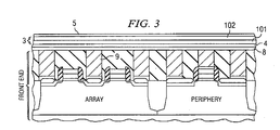
- the PZT layer, 3, formed during this deposition process has two PZT films, namely a stoichiometric film, 101, and a lead rich film, 102.
- a stoichiometric PZT film, 101 is now formed (step 208) over the bottom electrode, 4.
- stoichiometric film 101 is formed by a deposition technique called metal organic chemical vapor deposition ("MOCVD").
- the MOCVD deposition process involves delivering PbO + ZrO 2 + TiO 2 into the deposition chamber containing the semiconductor wafer, 2, to create a Pb(ZrTi)O 3 film.
- the MOCVD may be performed using a machine such as the Centura manufactured by AMAT (Applied Materials).
- AMAT Applied Materials
- another technique such as chemical solution deposition (sol-gel or metal organic decomposition) can also be used.
- the Zr to Ti ratio is 20/80; alternatively, pure PbTiO 3 may be used (to maximize switched polarization), or PbZrO 3 may be used - depending on the electronic device.
- the MOCVD deposition process for the PZT film, 101 is done at a wafer temperature of approximately 600°C, a deposition pressure of 8 Torr, with a precursor flow of 200mg/min, and a deposition rate of 140 ⁇ /min.
- the wafer temperature may be anything below 700°C
- the pressure may be anything greater than 2 Torr
- the precursor flow can be anything greater than 100 mg/min
- the deposition rate can be anything greater than 80 ⁇ /min.
- an Ar or He carrier gas is used to deliver the precursors to the reactor chamber through the showerhead where they are mixed with an oxidizer such as O 2 .
- an oxidizer such as O 2 .
- N 2 O or O 3 may be used as the oxidizer.
- the PZT film, 101 created by this process is stoichiometric (i.e. haze free and phase pure).
- the Pb content of the film may be from Pb 0.98 (Zr,Ti)O 3 to Pb 1.0 (Zr,Ti)O 3 .
- Film 101 is generally 50-100 ⁇ thick. However, it is within the scope of the invention to have a stoichiometric film, 101, with a thickness anywhere between 50-1400 ⁇ .
- the PZT film, 101 may be doped with up to 5% donor dopant. The donor dopant improves the reliability of the PZT by helping to control the point defect concentrations.
- a lead rich film of PZT, 102 is now formed (step 210) over the haze free, phase pure PZT film, 101.
- the lead rich film, 102 is also formed by MOCVD.
- another technique such as chemical solution deposition (sol-gel or metal organic decomposition) can also be used.
- the MOCVD deposition process of lead rich film, 102 involves delivering PbO + Zr0 2 + TiO 2 into the deposition chamber containing the semiconductor wafer, 2.
- the Zr to Ti ratio is 20/80; alternatively, pure PbTiO 3 may be used (to maximize switched polarization), or PbZrO 3 may be used - depending on the electronic device.
- the content of Pb is Pb 1.02 (Zr,Ti)O 3 ; however the amount of Pb can range from 1 to 1.02.
- the lead rich PZT film, 102 may be doped with up to 5% donor dopant. The donor dopant improves the reliability of the PZT by helping to control the point defect concentrations.
- the MOCVD deposition process for the PZT film, 102 is done at a wafer temperature of approximately 600°C, a deposition pressure of 8 Torr, with a precursor flow of 200mg/min, and a deposition rate of 140 ⁇ /min.
- wafer temperatures may be anything below 700°C
- the pressure may be anything greater than 2 Torr
- the precursor flow can be anything greater than 100 mg/min
- the deposition rate can be anything greater than 80 ⁇ /min.
- an Ar or He carrier gas is used to deliver the precursors to the reactor chamber through the showerhead where they are mixed with an oxidizer such as O 2 .
- an oxidizer such as O 2 .
- N 2 O or O 3 may be used as the oxidizer.
- the PZT layer, 102, created by this process is lead rich. However it is also haze free and phase pure because it was deposited on top of the perovskite film, 101. Film 102 is generally 600-650 ⁇ thick. (As an example, if the PZT layer, 3, is 700 ⁇ and the stoichiometric film, 101, is 50 ⁇ ; then the lead rich film, 102, is 650 ⁇ .) However, it is within the scope of the invention to have a lead rich PZT film, 102, with a thickness anywhere between 0-1400 ⁇ .
- the stoichiometric PZT film, 101, and the lead rich PZT film, 102 comprise the lead rich ferroelectric capacitor dielectric layer, 3. It is within the scope of the invention to use any combination of the above inventive techniques to create the high lead content capacitor dielectric layer, 3.
- the lead rich dielectric layer, 3, may be created using only the two film structure, using the two film structure manufactured using an increased deposition pressure (i.e. changing from 2 Torr to 4 Torr), or using the two film structure manufactured with an increased precursor flow (i.e. changing form 100mg/min to 200mg/min).
- the high lead content PZT dielectric layer, 3, will cause the ferroelectric capacitor to have desirable endurance, durability, and reliability.
- the haze free, phase pure PZT film, 3, formed in accordance with the present invention will operate at a lower operating voltage and therefore reduce the power consumption of electronic devices.
- the top electrode, 5, is formed (step 212) on the capacitor dielectric layer, 3.
- the top electrode, 5, is formed by sputter deposition of Ir (using Ar as the inert gas, but other inert gases may be used).
- the top electrode, 5, may be formed by reactive sputter deposition of IrO x (using (Ar+0 2 ) as the gas mixture, but inert gases other than Ar may be used in the mixture).
- other deposition techniques may be used to form the top electrode, 5, such as chemical vapor deposition.
- other materials may be used for the top electrode, such as Pt, Pd, PdOx, Au, Ru, RuOx, Rh, or RhOx.
- the entire capacitor stack (comprised of barrier, 8, bottom electrode, 4, capacitor dielectric, 3, and tope electrode, 5) is patterned, etched, and cleaned to form (step 214) the final ferroelectric capacitor structure.
- the formation (step 216) of the final electronic device structure continues, including the completion of the FeRAM module and the back-end module.
- the instant invention can be used to fabricate stand-alone FeRAM devices or FeRAM devices integrated into a semiconductor chip that has many other device functions than those described herein.
- the bottom electrode, 4, instead of forming the bottom electrode, 4, on the barrier layer, 8; the bottom electrode, 4, may be formed directly on the front-end module.
- this invention description focuses on the formation of planar capacitors, a three-dimensional capacitor using a post or cup structure can be fabricated with the same inventive process.
- the invention is applicable to semiconductor wafers having different well and substrate technologies, transistor configurations, and metal connector materials or configurations.
- the invention is applicable to other semiconductor technologies such as BiCMOS, bipolar, SOI, strained silicon, pyroelectric sensors, opto-electronic devices, microelectrical mechanical system (“MEMS”), or SiGe.
- MEMS microelectrical mechanical system
Landscapes
- Chemical & Material Sciences (AREA)
- Mechanical Engineering (AREA)
- General Chemical & Material Sciences (AREA)
- Chemical Kinetics & Catalysis (AREA)
- Engineering & Computer Science (AREA)
- Materials Engineering (AREA)
- Inorganic Chemistry (AREA)
- Metallurgy (AREA)
- Organic Chemistry (AREA)
- Semiconductor Memories (AREA)
- Inorganic Compounds Of Heavy Metals (AREA)
- Formation Of Insulating Films (AREA)
- Inorganic Insulating Materials (AREA)
Applications Claiming Priority (2)
| Application Number | Priority Date | Filing Date | Title |
|---|---|---|---|
| US356092 | 1982-03-08 | ||
| US10/356,092 US20040152214A1 (en) | 2003-01-30 | 2003-01-30 | Method of making a haze free, lead rich PZT film |
Publications (2)
| Publication Number | Publication Date |
|---|---|
| EP1443545A2 true EP1443545A2 (de) | 2004-08-04 |
| EP1443545A3 EP1443545A3 (de) | 2009-07-22 |
Family
ID=32655597
Family Applications (1)
| Application Number | Title | Priority Date | Filing Date |
|---|---|---|---|
| EP04002053A Withdrawn EP1443545A3 (de) | 2003-01-30 | 2004-01-30 | Herstellung eines Schleierfreien Bleireichen PZT-Films |
Country Status (3)
| Country | Link |
|---|---|
| US (2) | US20040152214A1 (de) |
| EP (1) | EP1443545A3 (de) |
| JP (1) | JP2004235645A (de) |
Families Citing this family (3)
| Publication number | Priority date | Publication date | Assignee | Title |
|---|---|---|---|---|
| JP4352271B2 (ja) * | 2006-06-09 | 2009-10-28 | セイコーエプソン株式会社 | 半導体装置 |
| JP5287175B2 (ja) * | 2008-11-26 | 2013-09-11 | 三菱電機株式会社 | 半導体装置の製造方法 |
| US8962350B2 (en) * | 2013-02-11 | 2015-02-24 | Texas Instruments Incorporated | Multi-step deposition of ferroelectric dielectric material |
Family Cites Families (11)
| Publication number | Priority date | Publication date | Assignee | Title |
|---|---|---|---|---|
| US5070026A (en) * | 1989-06-26 | 1991-12-03 | Spire Corporation | Process of making a ferroelectric electronic component and product |
| JPH0799252A (ja) * | 1993-06-22 | 1995-04-11 | Sharp Corp | 強誘電体膜の製造方法及びそれを用いた半導体装置 |
| US6080499A (en) * | 1997-07-18 | 2000-06-27 | Ramtron International Corporation | Multi-layer approach for optimizing ferroelectric film performance |
| JPH11195768A (ja) * | 1997-10-22 | 1999-07-21 | Fujitsu Ltd | ペロブスカイト型酸化物膜を含む電子装置とその製造方法及び強誘電体キャパシタ |
| KR100275726B1 (ko) * | 1997-12-31 | 2000-12-15 | 윤종용 | 강유전체 메모리 장치 및 그 제조 방법 |
| JPH11330411A (ja) * | 1998-05-13 | 1999-11-30 | Matsushita Electric Ind Co Ltd | 半導体記憶装置及びその製造方法 |
| US6586790B2 (en) * | 1998-07-24 | 2003-07-01 | Kabushiki Kaisha Toshiba | Semiconductor device and method for manufacturing the same |
| US6444478B1 (en) * | 1999-08-31 | 2002-09-03 | Micron Technology, Inc. | Dielectric films and methods of forming same |
| JP2001196547A (ja) * | 2000-01-12 | 2001-07-19 | Fujitsu Ltd | 半導体装置 |
| JP2001313429A (ja) * | 2000-04-27 | 2001-11-09 | Tdk Corp | 積層薄膜その製造方法および電子デバイス |
| US6887716B2 (en) * | 2000-12-20 | 2005-05-03 | Fujitsu Limited | Process for producing high quality PZT films for ferroelectric memory integrated circuits |
-
2003
- 2003-01-30 US US10/356,092 patent/US20040152214A1/en not_active Abandoned
-
2004
- 2004-01-29 JP JP2004020653A patent/JP2004235645A/ja not_active Abandoned
- 2004-01-30 EP EP04002053A patent/EP1443545A3/de not_active Withdrawn
-
2005
- 2005-01-28 US US11/046,568 patent/US7361949B2/en not_active Expired - Lifetime
Also Published As
| Publication number | Publication date |
|---|---|
| US7361949B2 (en) | 2008-04-22 |
| EP1443545A3 (de) | 2009-07-22 |
| US20040152214A1 (en) | 2004-08-05 |
| US20050130328A1 (en) | 2005-06-16 |
| JP2004235645A (ja) | 2004-08-19 |
Similar Documents
| Publication | Publication Date | Title |
|---|---|---|
| KR100275726B1 (ko) | 강유전체 메모리 장치 및 그 제조 방법 | |
| KR101101566B1 (ko) | 반도체 장치 및 그 제조 방법 | |
| US6855974B2 (en) | Ferroelectric capacitor, process for production thereof and semiconductor device using the same | |
| US20060073613A1 (en) | Ferroelectric memory cells and methods for fabricating ferroelectric memory cells and ferroelectric capacitors thereof | |
| US20020164850A1 (en) | Single transistor rare earth manganite ferroelectric nonvolatile memory cell | |
| KR19990013720A (ko) | 강유전체 캐패시터와 그 제조 방법 및 그 캐패시터를이용한 메모리셀 | |
| US20080061331A1 (en) | Semiconductor device and manufacturing method thereof | |
| US7910968B2 (en) | Semiconductor device and method for manufacturing the same | |
| JP7015011B2 (ja) | 強誘電性誘電材料の多段階堆積 | |
| US6326216B1 (en) | Process for producing semiconductor integrated circuit device | |
| JP2002176149A (ja) | 半導体記憶素子およびその製造方法 | |
| KR20030041974A (ko) | 단일 트랜지스터 희토류 망가나이트 강유전성 비휘발성메모리 셀 | |
| US8664011B2 (en) | Semiconductor device and method of manufacturing the semiconductor device | |
| WO2002011192A1 (en) | Integrated capacitive device with hydrogen degradable dielectric layer protected by getter layer | |
| US20050230725A1 (en) | Ferroelectric capacitor having an oxide electrode template and a method of manufacture therefor | |
| US20080123243A1 (en) | Ferroelectric capacitor | |
| US7012292B1 (en) | Oxidative top electrode deposition process, and microelectronic device structure | |
| US20150221516A1 (en) | Process-compatible sputtering target for forming ferroelectric memory capacitor plates | |
| US20040237998A1 (en) | FRAM capacitor stack clean | |
| JP3641142B2 (ja) | 強誘電体メモリ | |
| US7361949B2 (en) | Method of making a haze free, lead rich PZT film | |
| US20040023416A1 (en) | Method for forming a paraelectric semiconductor device | |
| US7049650B1 (en) | Semiconductor device | |
| US20040152216A1 (en) | Method of making a haze free PZT film | |
| US20050274999A1 (en) | Semiconductor device and method of manufacturing the same |
Legal Events
| Date | Code | Title | Description |
|---|---|---|---|
| PUAI | Public reference made under article 153(3) epc to a published international application that has entered the european phase |
Free format text: ORIGINAL CODE: 0009012 |
|
| AK | Designated contracting states |
Kind code of ref document: A2 Designated state(s): AT BE BG CH CY CZ DE DK EE ES FI FR GB GR HU IE IT LI LU MC NL PT RO SE SI SK TR |
|
| AX | Request for extension of the european patent |
Extension state: AL LT LV MK |
|
| PUAL | Search report despatched |
Free format text: ORIGINAL CODE: 0009013 |
|
| AK | Designated contracting states |
Kind code of ref document: A3 Designated state(s): AT BE BG CH CY CZ DE DK EE ES FI FR GB GR HU IE IT LI LU MC NL PT RO SE SI SK TR |
|
| AX | Request for extension of the european patent |
Extension state: AL LT LV MK |
|
| 17P | Request for examination filed |
Effective date: 20100122 |
|
| AKX | Designation fees paid |
Designated state(s): DE FR GB |
|
| 17Q | First examination report despatched |
Effective date: 20100427 |
|
| RBV | Designated contracting states (corrected) |
Designated state(s): DE FR GB NL |
|
| STAA | Information on the status of an ep patent application or granted ep patent |
Free format text: STATUS: THE APPLICATION IS DEEMED TO BE WITHDRAWN |
|
| 18D | Application deemed to be withdrawn |
Effective date: 20100908 |