EP1441426A1 - Method for fabricating semiconductor light emitting element, semiconductor light emitting element, method for fabricating semiconductor element, semiconductor element, method for fabricating element and element - Google Patents
Method for fabricating semiconductor light emitting element, semiconductor light emitting element, method for fabricating semiconductor element, semiconductor element, method for fabricating element and element Download PDFInfo
- Publication number
- EP1441426A1 EP1441426A1 EP02772973A EP02772973A EP1441426A1 EP 1441426 A1 EP1441426 A1 EP 1441426A1 EP 02772973 A EP02772973 A EP 02772973A EP 02772973 A EP02772973 A EP 02772973A EP 1441426 A1 EP1441426 A1 EP 1441426A1
- Authority
- EP
- European Patent Office
- Prior art keywords
- regions
- region
- substrate
- light emitting
- manufacturing
- Prior art date
- Legal status (The legal status is an assumption and is not a legal conclusion. Google has not performed a legal analysis and makes no representation as to the accuracy of the status listed.)
- Granted
Links
Images














Classifications
-
- C—CHEMISTRY; METALLURGY
- C30—CRYSTAL GROWTH
- C30B—SINGLE-CRYSTAL GROWTH; UNIDIRECTIONAL SOLIDIFICATION OF EUTECTIC MATERIAL OR UNIDIRECTIONAL DEMIXING OF EUTECTOID MATERIAL; REFINING BY ZONE-MELTING OF MATERIAL; PRODUCTION OF A HOMOGENEOUS POLYCRYSTALLINE MATERIAL WITH DEFINED STRUCTURE; SINGLE CRYSTALS OR HOMOGENEOUS POLYCRYSTALLINE MATERIAL WITH DEFINED STRUCTURE; AFTER-TREATMENT OF SINGLE CRYSTALS OR A HOMOGENEOUS POLYCRYSTALLINE MATERIAL WITH DEFINED STRUCTURE; APPARATUS THEREFOR
- C30B25/00—Single-crystal growth by chemical reaction of reactive gases, e.g. chemical vapour-deposition growth
- C30B25/02—Epitaxial-layer growth
-
- B—PERFORMING OPERATIONS; TRANSPORTING
- B82—NANOTECHNOLOGY
- B82Y—SPECIFIC USES OR APPLICATIONS OF NANOSTRUCTURES; MEASUREMENT OR ANALYSIS OF NANOSTRUCTURES; MANUFACTURE OR TREATMENT OF NANOSTRUCTURES
- B82Y20/00—Nanooptics, e.g. quantum optics or photonic crystals
-
- C—CHEMISTRY; METALLURGY
- C30—CRYSTAL GROWTH
- C30B—SINGLE-CRYSTAL GROWTH; UNIDIRECTIONAL SOLIDIFICATION OF EUTECTIC MATERIAL OR UNIDIRECTIONAL DEMIXING OF EUTECTOID MATERIAL; REFINING BY ZONE-MELTING OF MATERIAL; PRODUCTION OF A HOMOGENEOUS POLYCRYSTALLINE MATERIAL WITH DEFINED STRUCTURE; SINGLE CRYSTALS OR HOMOGENEOUS POLYCRYSTALLINE MATERIAL WITH DEFINED STRUCTURE; AFTER-TREATMENT OF SINGLE CRYSTALS OR A HOMOGENEOUS POLYCRYSTALLINE MATERIAL WITH DEFINED STRUCTURE; APPARATUS THEREFOR
- C30B29/00—Single crystals or homogeneous polycrystalline material with defined structure characterised by the material or by their shape
- C30B29/10—Inorganic compounds or compositions
- C30B29/40—AIIIBV compounds wherein A is B, Al, Ga, In or Tl and B is N, P, As, Sb or Bi
- C30B29/403—AIII-nitrides
-
- C—CHEMISTRY; METALLURGY
- C30—CRYSTAL GROWTH
- C30B—SINGLE-CRYSTAL GROWTH; UNIDIRECTIONAL SOLIDIFICATION OF EUTECTIC MATERIAL OR UNIDIRECTIONAL DEMIXING OF EUTECTOID MATERIAL; REFINING BY ZONE-MELTING OF MATERIAL; PRODUCTION OF A HOMOGENEOUS POLYCRYSTALLINE MATERIAL WITH DEFINED STRUCTURE; SINGLE CRYSTALS OR HOMOGENEOUS POLYCRYSTALLINE MATERIAL WITH DEFINED STRUCTURE; AFTER-TREATMENT OF SINGLE CRYSTALS OR A HOMOGENEOUS POLYCRYSTALLINE MATERIAL WITH DEFINED STRUCTURE; APPARATUS THEREFOR
- C30B29/00—Single crystals or homogeneous polycrystalline material with defined structure characterised by the material or by their shape
- C30B29/10—Inorganic compounds or compositions
- C30B29/40—AIIIBV compounds wherein A is B, Al, Ga, In or Tl and B is N, P, As, Sb or Bi
- C30B29/403—AIII-nitrides
- C30B29/406—Gallium nitride
-
- H—ELECTRICITY
- H01—ELECTRIC ELEMENTS
- H01S—DEVICES USING THE PROCESS OF LIGHT AMPLIFICATION BY STIMULATED EMISSION OF RADIATION [LASER] TO AMPLIFY OR GENERATE LIGHT; DEVICES USING STIMULATED EMISSION OF ELECTROMAGNETIC RADIATION IN WAVE RANGES OTHER THAN OPTICAL
- H01S5/00—Semiconductor lasers
- H01S5/30—Structure or shape of the active region; Materials used for the active region
- H01S5/32—Structure or shape of the active region; Materials used for the active region comprising PN junctions, e.g. hetero- or double- heterostructures
- H01S5/323—Structure or shape of the active region; Materials used for the active region comprising PN junctions, e.g. hetero- or double- heterostructures in AIIIBV compounds, e.g. AlGaAs-laser, InP-based laser
- H01S5/32308—Structure or shape of the active region; Materials used for the active region comprising PN junctions, e.g. hetero- or double- heterostructures in AIIIBV compounds, e.g. AlGaAs-laser, InP-based laser emitting light at a wavelength less than 900 nm
- H01S5/32341—Structure or shape of the active region; Materials used for the active region comprising PN junctions, e.g. hetero- or double- heterostructures in AIIIBV compounds, e.g. AlGaAs-laser, InP-based laser emitting light at a wavelength less than 900 nm blue laser based on GaN or GaP
-
- H—ELECTRICITY
- H01—ELECTRIC ELEMENTS
- H01S—DEVICES USING THE PROCESS OF LIGHT AMPLIFICATION BY STIMULATED EMISSION OF RADIATION [LASER] TO AMPLIFY OR GENERATE LIGHT; DEVICES USING STIMULATED EMISSION OF ELECTROMAGNETIC RADIATION IN WAVE RANGES OTHER THAN OPTICAL
- H01S5/00—Semiconductor lasers
- H01S5/30—Structure or shape of the active region; Materials used for the active region
- H01S5/34—Structure or shape of the active region; Materials used for the active region comprising quantum well or superlattice structures, e.g. single quantum well [SQW] lasers, multiple quantum well [MQW] lasers or graded index separate confinement heterostructure [GRINSCH] lasers
- H01S5/343—Structure or shape of the active region; Materials used for the active region comprising quantum well or superlattice structures, e.g. single quantum well [SQW] lasers, multiple quantum well [MQW] lasers or graded index separate confinement heterostructure [GRINSCH] lasers in AIIIBV compounds, e.g. AlGaAs-laser, InP-based laser
- H01S5/34333—Structure or shape of the active region; Materials used for the active region comprising quantum well or superlattice structures, e.g. single quantum well [SQW] lasers, multiple quantum well [MQW] lasers or graded index separate confinement heterostructure [GRINSCH] lasers in AIIIBV compounds, e.g. AlGaAs-laser, InP-based laser with a well layer based on Ga(In)N or Ga(In)P, e.g. blue laser
-
- H—ELECTRICITY
- H10—SEMICONDUCTOR DEVICES; ELECTRIC SOLID-STATE DEVICES NOT OTHERWISE PROVIDED FOR
- H10H—INORGANIC LIGHT-EMITTING SEMICONDUCTOR DEVICES HAVING POTENTIAL BARRIERS
- H10H20/00—Individual inorganic light-emitting semiconductor devices having potential barriers, e.g. light-emitting diodes [LED]
- H10H20/01—Manufacture or treatment
-
- H—ELECTRICITY
- H10—SEMICONDUCTOR DEVICES; ELECTRIC SOLID-STATE DEVICES NOT OTHERWISE PROVIDED FOR
- H10H—INORGANIC LIGHT-EMITTING SEMICONDUCTOR DEVICES HAVING POTENTIAL BARRIERS
- H10H20/00—Individual inorganic light-emitting semiconductor devices having potential barriers, e.g. light-emitting diodes [LED]
- H10H20/01—Manufacture or treatment
- H10H20/011—Manufacture or treatment of bodies, e.g. forming semiconductor layers
- H10H20/013—Manufacture or treatment of bodies, e.g. forming semiconductor layers having light-emitting regions comprising only Group III-V materials
- H10H20/0133—Manufacture or treatment of bodies, e.g. forming semiconductor layers having light-emitting regions comprising only Group III-V materials with a substrate not being Group III-V materials
- H10H20/01335—Manufacture or treatment of bodies, e.g. forming semiconductor layers having light-emitting regions comprising only Group III-V materials with a substrate not being Group III-V materials the light-emitting regions comprising nitride materials
-
- H—ELECTRICITY
- H10—SEMICONDUCTOR DEVICES; ELECTRIC SOLID-STATE DEVICES NOT OTHERWISE PROVIDED FOR
- H10H—INORGANIC LIGHT-EMITTING SEMICONDUCTOR DEVICES HAVING POTENTIAL BARRIERS
- H10H20/00—Individual inorganic light-emitting semiconductor devices having potential barriers, e.g. light-emitting diodes [LED]
- H10H20/80—Constructional details
- H10H20/81—Bodies
- H10H20/8215—Bodies characterised by crystalline imperfections, e.g. dislocations; characterised by the distribution of dopants, e.g. delta-doping
-
- H—ELECTRICITY
- H01—ELECTRIC ELEMENTS
- H01S—DEVICES USING THE PROCESS OF LIGHT AMPLIFICATION BY STIMULATED EMISSION OF RADIATION [LASER] TO AMPLIFY OR GENERATE LIGHT; DEVICES USING STIMULATED EMISSION OF ELECTROMAGNETIC RADIATION IN WAVE RANGES OTHER THAN OPTICAL
- H01S2301/00—Functional characteristics
- H01S2301/17—Semiconductor lasers comprising special layers
- H01S2301/173—The laser chip comprising special buffer layers, e.g. dislocation prevention or reduction
-
- H—ELECTRICITY
- H01—ELECTRIC ELEMENTS
- H01S—DEVICES USING THE PROCESS OF LIGHT AMPLIFICATION BY STIMULATED EMISSION OF RADIATION [LASER] TO AMPLIFY OR GENERATE LIGHT; DEVICES USING STIMULATED EMISSION OF ELECTROMAGNETIC RADIATION IN WAVE RANGES OTHER THAN OPTICAL
- H01S5/00—Semiconductor lasers
- H01S5/02—Structural details or components not essential to laser action
- H01S5/0206—Substrates, e.g. growth, shape, material, removal or bonding
- H01S5/0207—Substrates having a special shape
-
- H—ELECTRICITY
- H01—ELECTRIC ELEMENTS
- H01S—DEVICES USING THE PROCESS OF LIGHT AMPLIFICATION BY STIMULATED EMISSION OF RADIATION [LASER] TO AMPLIFY OR GENERATE LIGHT; DEVICES USING STIMULATED EMISSION OF ELECTROMAGNETIC RADIATION IN WAVE RANGES OTHER THAN OPTICAL
- H01S5/00—Semiconductor lasers
- H01S5/02—Structural details or components not essential to laser action
- H01S5/0206—Substrates, e.g. growth, shape, material, removal or bonding
- H01S5/0213—Sapphire, quartz or diamond based substrates
-
- H—ELECTRICITY
- H01—ELECTRIC ELEMENTS
- H01S—DEVICES USING THE PROCESS OF LIGHT AMPLIFICATION BY STIMULATED EMISSION OF RADIATION [LASER] TO AMPLIFY OR GENERATE LIGHT; DEVICES USING STIMULATED EMISSION OF ELECTROMAGNETIC RADIATION IN WAVE RANGES OTHER THAN OPTICAL
- H01S5/00—Semiconductor lasers
- H01S5/20—Structure or shape of the semiconductor body to guide the optical wave ; Confining structures perpendicular to the optical axis, e.g. index or gain guiding, stripe geometry, broad area lasers, gain tailoring, transverse or lateral reflectors, special cladding structures, MQW barrier reflection layers
- H01S5/2036—Broad area lasers
-
- H—ELECTRICITY
- H01—ELECTRIC ELEMENTS
- H01S—DEVICES USING THE PROCESS OF LIGHT AMPLIFICATION BY STIMULATED EMISSION OF RADIATION [LASER] TO AMPLIFY OR GENERATE LIGHT; DEVICES USING STIMULATED EMISSION OF ELECTROMAGNETIC RADIATION IN WAVE RANGES OTHER THAN OPTICAL
- H01S5/00—Semiconductor lasers
- H01S5/20—Structure or shape of the semiconductor body to guide the optical wave ; Confining structures perpendicular to the optical axis, e.g. index or gain guiding, stripe geometry, broad area lasers, gain tailoring, transverse or lateral reflectors, special cladding structures, MQW barrier reflection layers
- H01S5/22—Structure or shape of the semiconductor body to guide the optical wave ; Confining structures perpendicular to the optical axis, e.g. index or gain guiding, stripe geometry, broad area lasers, gain tailoring, transverse or lateral reflectors, special cladding structures, MQW barrier reflection layers having a ridge or stripe structure
-
- H—ELECTRICITY
- H01—ELECTRIC ELEMENTS
- H01S—DEVICES USING THE PROCESS OF LIGHT AMPLIFICATION BY STIMULATED EMISSION OF RADIATION [LASER] TO AMPLIFY OR GENERATE LIGHT; DEVICES USING STIMULATED EMISSION OF ELECTROMAGNETIC RADIATION IN WAVE RANGES OTHER THAN OPTICAL
- H01S5/00—Semiconductor lasers
- H01S5/20—Structure or shape of the semiconductor body to guide the optical wave ; Confining structures perpendicular to the optical axis, e.g. index or gain guiding, stripe geometry, broad area lasers, gain tailoring, transverse or lateral reflectors, special cladding structures, MQW barrier reflection layers
- H01S5/22—Structure or shape of the semiconductor body to guide the optical wave ; Confining structures perpendicular to the optical axis, e.g. index or gain guiding, stripe geometry, broad area lasers, gain tailoring, transverse or lateral reflectors, special cladding structures, MQW barrier reflection layers having a ridge or stripe structure
- H01S5/2201—Structure or shape of the semiconductor body to guide the optical wave ; Confining structures perpendicular to the optical axis, e.g. index or gain guiding, stripe geometry, broad area lasers, gain tailoring, transverse or lateral reflectors, special cladding structures, MQW barrier reflection layers having a ridge or stripe structure in a specific crystallographic orientation
-
- H—ELECTRICITY
- H01—ELECTRIC ELEMENTS
- H01S—DEVICES USING THE PROCESS OF LIGHT AMPLIFICATION BY STIMULATED EMISSION OF RADIATION [LASER] TO AMPLIFY OR GENERATE LIGHT; DEVICES USING STIMULATED EMISSION OF ELECTROMAGNETIC RADIATION IN WAVE RANGES OTHER THAN OPTICAL
- H01S5/00—Semiconductor lasers
- H01S5/20—Structure or shape of the semiconductor body to guide the optical wave ; Confining structures perpendicular to the optical axis, e.g. index or gain guiding, stripe geometry, broad area lasers, gain tailoring, transverse or lateral reflectors, special cladding structures, MQW barrier reflection layers
- H01S5/22—Structure or shape of the semiconductor body to guide the optical wave ; Confining structures perpendicular to the optical axis, e.g. index or gain guiding, stripe geometry, broad area lasers, gain tailoring, transverse or lateral reflectors, special cladding structures, MQW barrier reflection layers having a ridge or stripe structure
- H01S5/223—Buried stripe structure
- H01S5/2231—Buried stripe structure with inner confining structure only between the active layer and the upper electrode
-
- H—ELECTRICITY
- H01—ELECTRIC ELEMENTS
- H01S—DEVICES USING THE PROCESS OF LIGHT AMPLIFICATION BY STIMULATED EMISSION OF RADIATION [LASER] TO AMPLIFY OR GENERATE LIGHT; DEVICES USING STIMULATED EMISSION OF ELECTROMAGNETIC RADIATION IN WAVE RANGES OTHER THAN OPTICAL
- H01S5/00—Semiconductor lasers
- H01S5/40—Arrangement of two or more semiconductor lasers, not provided for in groups H01S5/02 - H01S5/30
- H01S5/4025—Array arrangements, e.g. constituted by discrete laser diodes or laser bar
- H01S5/4031—Edge-emitting structures
-
- H—ELECTRICITY
- H10—SEMICONDUCTOR DEVICES; ELECTRIC SOLID-STATE DEVICES NOT OTHERWISE PROVIDED FOR
- H10H—INORGANIC LIGHT-EMITTING SEMICONDUCTOR DEVICES HAVING POTENTIAL BARRIERS
- H10H20/00—Individual inorganic light-emitting semiconductor devices having potential barriers, e.g. light-emitting diodes [LED]
- H10H20/80—Constructional details
- H10H20/81—Bodies
- H10H20/822—Materials of the light-emitting regions
- H10H20/824—Materials of the light-emitting regions comprising only Group III-V materials, e.g. GaP
- H10H20/825—Materials of the light-emitting regions comprising only Group III-V materials, e.g. GaP containing nitrogen, e.g. GaN
-
- H—ELECTRICITY
- H10—SEMICONDUCTOR DEVICES; ELECTRIC SOLID-STATE DEVICES NOT OTHERWISE PROVIDED FOR
- H10P—GENERIC PROCESSES OR APPARATUS FOR THE MANUFACTURE OR TREATMENT OF DEVICES COVERED BY CLASS H10
- H10P14/00—Formation of materials, e.g. in the shape of layers or pillars
- H10P14/20—Formation of materials, e.g. in the shape of layers or pillars of semiconductor materials
- H10P14/24—Formation of materials, e.g. in the shape of layers or pillars of semiconductor materials using chemical vapour deposition [CVD]
-
- H—ELECTRICITY
- H10—SEMICONDUCTOR DEVICES; ELECTRIC SOLID-STATE DEVICES NOT OTHERWISE PROVIDED FOR
- H10P—GENERIC PROCESSES OR APPARATUS FOR THE MANUFACTURE OR TREATMENT OF DEVICES COVERED BY CLASS H10
- H10P14/00—Formation of materials, e.g. in the shape of layers or pillars
- H10P14/20—Formation of materials, e.g. in the shape of layers or pillars of semiconductor materials
- H10P14/34—Deposited materials, e.g. layers
- H10P14/3402—Deposited materials, e.g. layers characterised by the chemical composition
- H10P14/3414—Deposited materials, e.g. layers characterised by the chemical composition being group IIIA-VIA materials
- H10P14/3416—Nitrides
-
- H—ELECTRICITY
- H10—SEMICONDUCTOR DEVICES; ELECTRIC SOLID-STATE DEVICES NOT OTHERWISE PROVIDED FOR
- H10P—GENERIC PROCESSES OR APPARATUS FOR THE MANUFACTURE OR TREATMENT OF DEVICES COVERED BY CLASS H10
- H10P14/00—Formation of materials, e.g. in the shape of layers or pillars
- H10P14/20—Formation of materials, e.g. in the shape of layers or pillars of semiconductor materials
- H10P14/38—Formation of materials, e.g. in the shape of layers or pillars of semiconductor materials characterised by treatments done after the formation of the materials
Definitions
- This invention relates to a method of manufacturing a semiconductor light emitting device, a semiconductor light emitting device, method of manufacturing a semiconductor device, a semiconductor device, a method of manufacturing a device, and a device itself, that are suitable for use in the manufacture of semiconductor lasers, light emitting diodes or electron transport devices composed of nitride III-V compound semiconductors, for example.
- substrates of semiconductor devices should preferably be made of materials that are common in nature to semiconductors used in devices and have low densities of dislocations or other defects. This is because defects of substrates are copied to semiconductor layers growing thereon and often invite deterioration of device properties.
- Nitride III-V compound semiconductors represented by GaN have large band gaps. For this advantage, they are under progressive development in form of light emitting elements for wavelength ranges from ultraviolet to violet, blue and green, which are difficult to obtain with other semiconductors. Actually, light emitting diodes (LEDs) and semiconductor lasers (LDs) using nitride III-V compound semiconductors have been brought into practice.
- LEDs light emitting diodes
- LDs semiconductor lasers
- nitride III-V compound semiconductors are difficult to form by bulk growth, and it has been difficult to obtain substrates reduced in defect to a level acceptable for use as substrates of semiconductor devices. Therefore, in almost all cases, nitride III-V compound semiconductors must be formed by crystalline growth on substrates of sapphire, SiC, or the like, that are different in nature from the nitride III-V compound semiconductors to be grown, and the process of forming low-temperature buffer layers is required. However, even through that process, nitride III-V compound semiconductors obtained by growth exhibit very high defect densities, and give considerable influences to device properties.
- JP-2001-102307 has proposed a method of manufacturing a single-crystal GaN substrate as a method of manufacturing a nitride III-V compound semiconductor substrate having a reduced density of defects.
- This method intends to reduce dislocations by controlling the growth surface of vapor-phase deposition to have a three-dimensional facet structure instead of a flat state and progressing growth while keeping the facet structure and not burying the facet structure.
- the technique disclosed by JP-2001-102307 concentrates breakthrough dislocations especially to certain regions of the growth layer and thereby reduces breakthrough dislocations of the other regions. Therefore, the single-crystal GaN substrate locally includes low defect density regions and high defect density regions. Moreover, it is out of control where the high defect density regions appear, and they appear at random. Therefore, in case a semiconductor device, such as a semiconductor laser, is manufactured by growth of nitride III-V compound semiconductor layers on the single-crystal GaN substrate, this technique cannot prevent a high defect density region from being formed in the emission region, and inevitably invites degradation of emission properties and reliability of semiconductor lasers.
- an object of the invention is to provide a semiconductor device improved in property, reliable and elongated in lifetime, as well as a method capable of manufacturing such a semiconductor device.
- an object of the invention is to provide various types of devices excellent in property, reliable and elongated in lifetime, as well as a method capable of manufacturing such devices.
- the Inventor conducted vigorous researches toward a solution of the above-mentioned objects.
- the researches are summarized below.
- the Inventor made improvements the technique disclosed by JP-2001-102307 over and over, and could make a success in controlling positions of high defect density regions appearing among low defect density regions. This makes it possible to obtain a substrate in which high defect density regions are appear regularly, for example periodically, among low defect density regions, and makes it possible to change the pattern of layout of high defect density regions as desired.
- high defect density regions can be controlled to appear regularly, it is possible to determine the size of devices, placement of devices or locations of active regions of the devices (for example, emission regions in case of light emitting devices) in accordance with the layout of the high defect density regions in the stage of their design.
- the design can be determined such that high defect density regions do not reside in regions that will be finally extracted as chips by dicing the substrate (called “device regions” hereunder) or in active regions of devices.
- the above-mentioned technique is effective also for manufacturing a semiconductor device using semiconductors other than nitride III-V compound semiconductors when it is difficult to obtain a substrate of the same nature as that of semiconductors used as a device and exhibiting a low defect density. More generally, in case a substrate of the same nature as that of the material used as a device and having a low defect density is difficult to obtain, the above-mentioned technique is effective for manufacturing the device.
- the present invention has been made after further studies by the Inventor based on the above-explained knowledge.
- the fist aspect of the invention is a method of manufacturing a semiconductor light emitting device by growing nitride III-V compound semiconductor layers forming a light emitting device structure on a nitride III-V compound semiconductor substrate in which a plurality of second regions having a second average dislocation density higher than a first average dislocation density align regularly in a first region made of a crystal and having the first average dislocation density, comprising:
- each device region may include second regions along the entire border lines thereof, but also means that the border lines of each device region may pass through second regions, and the second regions may remain on end surfaces or at corners of chips obtained by dicing the substrate (also in the description hereunder).
- device regions are determined in size and layout not to include second regions substantially.
- a plurality of second regions are typically formed periodically, for example, in form of hexagonal lattices, rectangular lattices, or square lattices. Two or more of these layout patterns may be mixed. It is also acceptable that the substrate includes a region where the second regions periodically appear and a region where the second regions appear regularly but not periodically.
- Each device region is typically rectangular or square.
- a pair of opposite sides of each device region are preferably parallel to the ⁇ 1-100> direction, and the other pair of opposite sides is parallel to the ⁇ 11-20> direction.
- Interval between two adjacent second regions or period of arrangement of the second regions is determined depending upon the size of devices. Typically, however, it is 20 ⁇ m or more, 50 ⁇ m or more, or 100 ⁇ m or more. There is no definite maximum value of the interval or period of the second regions. Typically, however, it is around 1000 ⁇ m in maximum.
- the second regions typically pass through the nitride III-V compound semiconductor substrate. Each of the second regions typically has an arbitrary polygonal prismatic shape.
- Third regions having a third average dislocation density higher than the first average dislocation density and lower than the second average dislocation density are often interposed between the first region and the second regions. In this case, each device region is most preferably defined not to contain the second and third regions substantially.
- Diameter of each second region is typically from 10 ⁇ m to 100 ⁇ m, or more typically from 20 ⁇ m to 50 ⁇ m.
- diameter of each third region is typically larger than the diameter of the second region by from 20 ⁇ m to 200 ⁇ m, more typically by from 40 ⁇ m to 160 ⁇ m, or most typically by from 60 ⁇ m to 140 ⁇ m.
- Average dislocation density of the second regions in general, is five times or more of the average dislocation density of the first region.
- average dislocation density of the first region is 2x10 6 cm -2 or less
- average dislocation density of the second regions is 1x10 8 cm -2 or more.
- its average dislocation density is typically smaller than 1x10 8 cm -2 and larger than 2x10 6 cm -2 .
- emission regions of semiconductor light emitting devices are distant from the second regions by 1 ⁇ m or more, preferably by 10 ⁇ m or more, or more preferably by 100 ⁇ m or more.
- the substrate includes the third regions, it is most preferable for the emission regions of the semiconductor light emitting devices to be off both the second and third regions.
- the semiconductor light emitting devices are semiconductor lasers or light emitting diodes.
- regions supplied with a drive current through a stripe-shaped electrode should be distant from the second regions preferably by 1 ⁇ m or more, more preferably by 10 ⁇ m or more, and still more preferably by 100 ⁇ m or more.
- the substrate includes the third regions, the regions supplied with a drive current through stripe-shaped electrodes should most preferably be off both the second regions and the third regions.
- the stripe-shaped electrode may be either singular or plural, and its width may be determined as desired.
- the border lines of each device region are determined to use the given area of the substrate efficiently, depending upon the layout pattern of the second regions, or their interval or period, to the extent ensuring that no device region includes the second regions substantially.
- the border lines of each device region are determined to include a straight line connecting at least two adjacent second regions.
- the nitride III-V compound semiconductor substrate having nitride III-V compound semiconductor layers grown thereon is preferably diced along such border lines each including the straight line connecting at least two adjacent second regions. The dicing typically relies on cleavage, but other methods using a diamond saw or a laser beam may be used alternatively for the same purpose.
- the border lines of each device region which includes a straight line connecting at least two adjacent second regions, facilitates desirable cleavage, because the second regions having an average dislocation density higher than that of the first region is weaker in mechanical strength than the first region. This is especially advantageous for obtaining desirable cavity edges of semiconductor lasers.
- the border lines of each device region may be determined not to pass any second regions. In this case, the border lines of each device region should preferably be distant from the second regions by at least 1 ⁇ m in order to minimize adverse influences of the second regions.
- the nitride III-V compound semiconductor substrate having nitride III-V compound semiconductor layers grown thereon is diced along the border lines distant inside from the second regions.
- the nitride III-V compound semiconductor substrate or the nitride III-V compound semiconductor layers are made of, most generally, Al x B y Ga 1-x-y-z In z As u N 1-u-v P v (where 0 ⁇ x ⁇ 1, 0 ⁇ y ⁇ 1, 0 ⁇ z ⁇ 1, 0 ⁇ u ⁇ 1, 0 ⁇ v ⁇ 1, 0 ⁇ x+y+z ⁇ 1 and 0 ⁇ u+v ⁇ 1), or more specifically, Al x B y Ga 1-x-y-z In z N (where 0 ⁇ x ⁇ 1, 0 ⁇ y ⁇ 1, 0 ⁇ z ⁇ 1 and 0 ⁇ x+y+z ⁇ 1). Typically, they are made of Al x Ga 1-x-z In z N (where 0 ⁇ x ⁇ 1 and 0 ⁇ z ⁇ 1). Most typically, the nitride III-V compound semiconductor substrate is made of GaN.
- the second aspect of the invention is a semiconductor light emitting device manufactured by:
- the third aspect of the invention is a semiconductor light emitting device including nitride III-V compound semiconductor layers grown to form a light emitting device structure on a nitride III-V compound substrate in which a plurality of second regions having a second average dislocation density higher than a first average dislocation density align regularly in a first region made of a crystal and having the first average dislocation density, in which at least one of said second regions resides on an end surface or a corner of the nitride III-V compound semiconductor substrate.
- the fourth aspect of the invention is method of manufacturing a semiconductor light emitting device by growing nitride III-V compound semiconductor layers forming a light emitting device structure on a nitride III-V compound semiconductor substrate in which a plurality of second regions having a second average defect density higher than a first average defect density align regularly in a first region made of a crystal and having the first average defect density, comprising:
- the fifth aspect of the invention is a semiconductor light emitting device manufactured by:
- the sixth aspect of the invention is a semiconductor light emitting device including nitride III-V compound semiconductor layers grown to form a light emitting device structure on a nitride III-V compound semiconductor substrate in which a plurality of second regions having a second average defect density higher than a first average defect density align regularly in a first region made of a crystal and having the first average defect density, in which at least one of said second regions resides on an end surface or a corner of the nitride III-V compound semiconductor substrate.
- the "average defect density” means the average density of entire lattice defects that will adversely affect the properties and reliability of the devices, and defects involve all kinds of defects such as dislocations, stacking faults and point defects, for example (also in the description hereunder).
- the seventh aspect of the invention is a method of manufacturing a semiconductor light emitting device by growing nitride III-V compound semiconductor layers forming a light emitting device structure on a nitride III-V compound semiconductor substrate in which a plurality of second regions inferior in crystalline property to a first region align regularly in the first region made of a crystal, comprising:
- the eighth aspect of the invention is a semiconductor light emitting device manufactured by:
- the ninth aspect of the invention is a semiconductor light emitting device including nitride III-V compound semiconductor layers grown to form a light emitting device structure on a nitride III-V compound substrate in which a plurality of second regions inferior in crystalline property to a first region align regularly in the first region made of a crystal, in which at least one of said second regions resides on an end surface or a corner of the nitride III-V compound semiconductor substrate.
- the crystal composing the first region is typically a single crystal
- the second regions inferior in crystallographic property to the first region are composed of a polycrystal, amorphous substance, or their mixture (also in the description hereunder).
- This relation corresponds to the relation between a lower average dislocation density or an average defect density of the second regions and a higher average dislocation density or an average defect density of the first region.
- the tenth aspect of the invention is a method of manufacturing a semiconductor device by growing nitride III-V compound semiconductor layers forming a device structure on a nitride III-V compound semiconductor substrate in which a plurality of second regions having a second average dislocation density higher than a first average dislocation density align regularly in a first region made of a crystal and having the first average dislocation density, comprising:
- the eleventh aspect of the invention is a semiconductor device manufactured by:
- the twelfth aspect of the invention is a semiconductor device including nitride III-V compound semiconductor layers grown to form a device structure on a nitride III-V compound semiconductor substrate in which a plurality of second regions having a second average dislocation density higher than a first average dislocation density align regularly in a first region made of a crystal and having the first average dislocation density, in which at least one of said second regions resides on an end surface or a corner of the nitride III-V compound semiconductor substrate.
- the semiconductor device may be a light emitting device such as a light emitting diode or a semiconductor laser, photodetector, or electron transport device such as a high electron mobility transistor or other type field effect transistor (FET) or a heterojunction bipolar transistor (HBT) (also in the description hereunder).
- a light emitting device such as a light emitting diode or a semiconductor laser, photodetector, or electron transport device such as a high electron mobility transistor or other type field effect transistor (FET) or a heterojunction bipolar transistor (HBT) (also in the description hereunder).
- FET field effect transistor
- HBT heterojunction bipolar transistor
- active regions of semiconductor devices are distant from the second regions by 1 ⁇ m or more, preferably by 10 ⁇ m or more, or more preferably by 100 ⁇ m or more.
- the substrate includes the third regions, it is most preferable for the active regions of the semiconductor devices to be off both the second and third regions.
- the active region herein means an emission region in case of a semiconductor light emitting device, a photo-detecting region in case of a semiconductor photodetector, and a region where electrons run in case of an electron transport device (also in the description hereunder).
- the thirteenth aspect of the invention is a method of manufacturing a semiconductor light emitting device by growing semiconductor layers forming a light emitting device structure on a semiconductor substrate in which a plurality of second regions having a second average dislocation density higher than a first average dislocation density align regularly in a first region made of a crystal and having the first average dislocation density, comprising:
- the fourteenth aspect of the invention is a semiconductor light emitting device manufactured by:
- the fifteenth aspect of the invention is a semiconductor light emitting device including semiconductor layers grown to form a light emitting device structure on a semiconductor substrate in which a plurality of second regions having a second average dislocation density higher than a first average dislocation density align regularly in a first region made of a crystal and having the first average dislocation density, in which at least one of said second regions resides on an end surface or a corner of the semiconductor substrate.
- the sixteenth aspect of the invention is a method of manufacturing a semiconductor device by growing semiconductor layers forming a device structure on a semiconductor substrate in which a plurality of second regions having a second average dislocation density higher than a first average dislocation density align regularly in a first region made of a crystal and having the first average dislocation density, comprising:
- the seventeenth aspect of the invention is a semiconductor device manufactured by:
- the eighteenth aspect of the invention is a semiconductor device including semiconductor layers grown to form a device structure on a semiconductor substrate in which a plurality of second regions having a second average dislocation density higher than a first average dislocation density align regularly in a first region made of a crystal and having the first average dislocation density, in which at least one of said second regions resides on an end surface or a corner of the semiconductor substrate.
- material of the semiconductor substrate or the semiconductor layers may be selected from nitride III-V compound semiconductors, other semiconductors having wurtzite structures, or more generally, hexagonal system crystal structures, such as ZnO, ⁇ -ZnS, ⁇ -CdS, ⁇ -CdSe, or the like, or other various semiconductors having other crystalline structures.
- the nineteenth aspect of the invention is a method of manufacturing a device by growing layers forming a device structure on a substrate in which a plurality of second regions having a second average dislocation density higher than a first average dislocation density align regularly in a first region made of a crystal and having the first average dislocation density, comprising:
- the twentieth aspect of the invention is a device manufactured by:
- the twenty-first aspect of the invention is a device including layers grown to form a device structure on a substrate in which a plurality of second regions having a second average dislocation density higher than a first average dislocation density align regularly in a first region made of a crystal and having the first average dislocation density, in which at least one of said second regions resides on an end surface or a corner of the substrate.
- the device may be a semiconductor device (light emitting device, photodetector electron transport device, etc.), piezoelectric element, pyroelectric device, optical device (such as secondary high-frequency generating device using a nonlinear optical crystal), dielectric device (contemplating a ferroelectric device as well), superconducting device), or the like.
- material of the substrate or layers may be selected from various semiconductors.
- piezoelectric device, pyroelectric device, optical device, dielectric device, superconducting device, etc various materials such as oxides, for example, may be used. There are lots of kinds of oxide materials including those disclosed in Journal of the Society of Japan Vol. 103, No. 11(1995) pp. 1099-1111 and Materials Science and Engineering B41 (1996) 166-173, for example.
- the twenty-second aspect of the invention is a method of manufacturing a device by growing layers forming a device structure on a substrate in which a plurality of second regions having a second average dislocation density higher than a first average dislocation density align regularly in a first region made of a crystal and having the first average dislocation density, comprising:
- the twenty-third aspect of the invention is a device including layers grown to form a device structure on a substrate in which a plurality of second regions having a second average dislocation density higher than a first average dislocation density align regularly in a first region made of a crystal and having the first average dislocation density, in which at least one of said second regions resides inside the substrate or on an end surface or a corner of the substrate, and an active region of the device does not include the second regions.
- the twenty-fourth aspect of the invention is a method of manufacturing a device by growing layers forming a device structure on a substrate in which a plurality of second regions having a second average defect density higher than a first average defect density align regularly in a first region made of a crystal and having the first average defect density, comprising:
- the twenty-fourth aspect of the invention is a device including layers grown to form a device structure on a substrate in which a plurality of second regions having a second average defect density higher than a first average defect density align regularly in a first region made of a crystal and having the first average defect density, in which at least one of said second regions resides inside the substrate or on an end surface or a corner of the substrate, and an active region of the device does not include the second regions.
- the twenty-sixth aspect of the invention is a method of manufacturing a device by growing layers forming a device structure on a substrate in which a plurality of second regions inferior in crystalline property to a first region align regularly in the first region made of a crystal, comprising:
- the twenty-seventh aspect of the invention is a device including layers grown to form a device structure on a substrate in which a plurality of second regions inferior in crystalline property to a first region align regularly in a first region made of a crystal, in which at least one of said second regions resides inside the substrate or on an end surface or a corner of the substrate, and an active region of the device does not include the second regions.
- the twenty-eighth aspect of the invention is a method of manufacturing a device by growing layers forming a device structure on a substrate in which a plurality of second regions having a second average dislocation density higher than a first average dislocation density regularly align in a first region having the first average dislocation density in first intervals in a first direction and in second intervals smaller than the first intervals in a second direction normal to the first direction, comprising:
- the twenty-ninth aspect of the invention is a device manufactured by growing layers forming a device structure on a substrate in which a plurality of second regions having a second average dislocation density higher than a first average dislocation density regularly align in a first region having the first average dislocation density in first intervals in a first direction and in second intervals smaller than the first intervals in a second direction normal to the first direction, in which the substrate does not substantially include seven or more rows of the second regions and an active region of the device does not include the second regions.
- the thirtieth aspects of the invention is a method of manufacturing a device by growing layers forming a device structure on a substrate in which a plurality of second regions having a second average defect density higher than a first average defect density regularly align in a first region having the first average defect density in first intervals in a first direction and in second intervals smaller than the first intervals in a second direction normal to the first direction, comprising:
- the thirty-first aspect of the invention is a device manufactured by growing layers forming a device structure on a substrate in which a plurality of second regions having a second average defect density higher than a first average defect density regularly align in a first region having the first average defect density in first intervals in a first direction and in second intervals smaller than the first intervals in a second direction normal to the first direction, in which the substrate does not substantially include seven or more rows of the second regions and an active region of the device does not include the second regions.
- the thirty-second aspect of the invention is a method of manufacturing a device by growing layers forming a device structure on a substrate in which a plurality of second regions inferior in crystalline property to a first region regularly align in a first region in first intervals in a first direction and in second intervals smaller than the first intervals in a second direction normal to the first direction, comprising:
- the thirty-third aspect of the invention is a device manufactured by growing layers forming a device structure on a substrate in which a plurality of second regions inferior in crystalline property to a first region regularly align in a first region in first intervals in a first direction and in second intervals smaller than the first intervals in a second direction normal to the first direction, in which the substrate does not substantially include seven or more rows of the second regions and an active region of the device does not include the second regions.
- the thirty-fourth aspect of the invention is a method of manufacturing a device by growing layers forming a device structure on a substrate in which a plurality of second regions having a second average dislocation density higher than a first average dislocation density regularly align in a first region having the first average dislocation density in first intervals in a first direction and in second intervals smaller than the first intervals in a second direction normal to the first direction, comprising:
- the thirty-fifth aspect of the invention is a device manufactured by growing layers forming a device structure on a substrate in which a plurality of second regions having a second average dislocation density higher than a first average dislocation density regularly align in a first region having the first average dislocation density in first intervals in a first direction and in second intervals smaller than the first intervals in a second direction normal to the first direction, in which the first interval is 50 ⁇ m or more, one or more rows of the second regions in the second direction is included, and an active region of the device does not include the second regions.
- the thirty-sixth aspect of the invention is a method of manufacturing a device by growing layers forming a device structure on a substrate in which a plurality of second regions having a second average defect density higher than a first average defect density regularly align in a first region having the first average defect density in first intervals in a first direction and in second intervals smaller than the first intervals in a second direction normal to the first direction, comprising:
- the thirty-seventh aspect of the invention is a device manufactured by growing layers forming a device structure on a substrate in which a plurality of second regions having a second average defect density higher than a first average defect density regularly align in a first region having the first average defect density in first intervals in a first direction and in second intervals smaller than the first intervals in a second direction normal to the first direction, in which the first interval is 50 ⁇ m or more, one or more rows of the second regions in the second direction is included, and an active region of the device does not include the second regions.
- the thirty-eighth aspect of the invention is a method of manufacturing a device by growing layers forming a device structure on a substrate in which a plurality of second regions inferior in crystalline property to a first region align in a first region in first intervals in a first direction and in second intervals smaller than the first intervals in a second direction normal to the first direction, comprising:
- the thirty-ninth aspect of the invention is a device manufactured by growing layers forming a device structure on a substrate in which a plurality of second regions inferior in crystalline property to a first region regularly align in a first region in first intervals in a first direction and in second intervals smaller than the first intervals in a second direction normal to the first direction, in which the first interval is 50 ⁇ m or more, one or more rows of the second regions in the second direction is included, and an active region of the device does not include the second regions.
- the fortieth aspect of the invention is a method of manufacturing a device by growing layers to form a device structure on a substrate in which a plurality of second regions having a second average dislocation density higher than a first average dislocation density and extending linearly align regularly in parallel to each other in a first region made of a crystal having the first average dislocation density, comprising:
- the forty-first aspect of the invention is a device manufactured by growing layers forming a device structure on a substrate in which a plurality of second regions having a second average dislocation density higher than a first average dislocation density and extending linearly align regularly in parallel to each other in a first region made of a crystal having the first average dislocation density, in which the device region does not substantially include seven or more rows of the second regions in the second direction, and an active region of the device does not include the second regions.
- the forty-second aspect of the invention is a method of manufacturing a device by growing layers to form a device structure on a substrate in which a plurality of second regions having a second average defect density higher than a first average defect density and extending linearly align regularly in parallel to each other in a first region made of a crystal having the first average defect density, comprising:
- the forty-third aspect of the invention is a device manufactured by growing layers forming a device structure on a substrate in which a plurality of second regions having a second average defect density higher than a first average defect density and extending linearly align regularly in parallel to each other in a first region made of a crystal having the first average defect density, in which the device region does not substantially include seven or more rows of the second regions in the second direction, and an active region of the device does not include the second regions.
- the forty-fourth aspect of the invention is a method of manufacturing a device by growing layers to form a device structure on a substrate in which a plurality of second regions inferior in crystalline property to a first region and extending linearly align regularly in parallel to each other in a first region made of a crystal, comprising:
- the forty-fifth aspect of the invention is a device manufactured by growing layers forming a device structure on a substrate in which a plurality of second regions inferior in crystalline property to a first region and extending linearly align regularly in parallel to each other in a first region made of a crystal, in which the device region does not substantially include seven or more rows of the second regions in the second direction, and an active region of the device does not include the second regions.
- the forty-sixth aspect of the invention is a method of manufacturing a device by growing layers to form a device structure on a substrate in which a plurality of second regions having a second average dislocation density higher than a first average dislocation density and extending linearly align regularly in parallel to each other in a first region made of a crystal having the first average dislocation density, comprising:
- the forty-seventh aspect of the invention is a device manufactured by growing layers forming a device structure on a substrate in which a plurality of second regions having a second average dislocation density higher than a first average dislocation density and extending linearly align regularly in parallel to each other in a first region made of a crystal having the first average dislocation density, in which the interval of the second regions is 50 ⁇ m or more, one or more of the second regions are included, and an active region of the device does not include the second regions.
- the forty-eighth aspect of the invention is a method of manufacturing a device by growing layers to form a device structure on a substrate in which a plurality of second regions having a second average defect density higher than a first average defect density and extending linearly align regularly in parallel to each other in a first region made of a crystal having the first average defect density, comprising:
- the forty-ninth aspect of the invention is a device manufactured by growing layers forming a device structure on a substrate in which a plurality of second regions having a second average defect density higher than a first average defect density and extending linearly align regularly in parallel to each other in a first region made of a crystal having the first average defect density, in which the interval of the second regions is 50 ⁇ m or more, one or more of the second regions are included, and an active region of the device does not include the second regions.
- the fiftieth aspect of the invention is a method of manufacturing a device by growing layers to form a device structure on a substrate in which a plurality of second regions inferior in crystalline property to a first region and extending linearly align regularly in parallel to each other in a first region made of a crystal, comprising:
- the fifty-first aspect of the invention is a device manufactured by growing layers forming a device structure on a substrate in which a plurality of second regions inferior in crystalline property to a first region and extending linearly align regularly in parallel to each other in a first region made of a crystal, in which the interval of the second regions is 50 ⁇ m or more, one or more of the second regions are included, and an active region of the device does not include the second regions.
- the interval of the second regions in the first direction (first interval) or the interval of the second regions extending straight are equivalent to the interval of the second regions or the alignment interval of the second regions set forth in conjunction with the first aspect of the invention.
- the interval of the second regions in the first direction (first interval) or the interval of the second regions extending straight are equivalent to the interval of the second regions or the alignment interval of the second regions set forth in conjunction with the first aspect of the invention excepting that its lower limit is 50 ⁇ m.
- the interval between the second regions in the second direction may be determined basically freely within the range smaller than the first distance. Although depending upon the size of each second region, the interval is generally from 10 ⁇ m to 1000 ⁇ m and typically from 20 ⁇ m to 200 ⁇ m. In the twenty-eighth to thirty-third aspects and fortieth to forty-fifth aspects of the invention, the number of rows of the second regions in the second direction or the number of second regions extending straight is limited to seven in maximum. This is because the device region may possibly include seven or so second regions in relation to the chip size of the device, depending upon the interval between the rows of the second regions in the second direction or between the second regions extending straight. The number of rows of the second regions in the second direction or the number of second regions extending straight is typically three or less in a semiconductor light emitting device usually having a small chip size.
- device regions are defined on the nitride III-V compound semiconductor substrate, other semiconductor substrate or any kind of substrate such that active regions of devices do not substantially include the second regions higher in average dislocation density, higher in average defect density or inferior in crystalline property to the first region. Therefore, even when some defects such as dislocations propagate to nitride III-V compound semiconductor layers, other semiconductor layers or layers of any other various kinds of materials that are deposited for forming light emitting structures or other device structures, it is ensured that chips obtained by dicing the substrate include substantially no dislocations or other defects.
- Figs. 1A and 1B are a perspective view and a cross-sectional view for explaining the essence of an embodiment of the invention
- Fig. 2 is a plan view for explaining the essence of an embodiment of the invention
- Fig. 3 is a plan view for explaining the essence of an embodiment of the invention
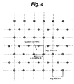
- Fig. 4 is a plan view for explaining the essence of an embodiment of the invention
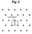
- Fig. 5 is a plan view for explaining the essence of an embodiment of the invention
- Fig. 6 is a plan view for explaining a method of manufacturing a GaN compound semiconductor laser according to the first embodiment of the invention
- Fig. 7 is a schematic diagram showing an exemplary distribution of dislocation density near a high defect region of a GaN substrate used in the first embodiment of the invention
- Fig. 7 is a schematic diagram showing an exemplary distribution of dislocation density near a high defect region of a GaN substrate used in the first embodiment of the invention
- Fig. 7 is a schematic diagram showing an exemplary distribution of dislocation density near a high defect
- FIG. 8 is a plan view for explaining the method of manufacturing the GaN compound semiconductor laser according to the first embodiment of the invention
- Fig. 9 is a cross-sectional view for explaining the method of manufacturing the GaN compound semiconductor laser according to the first embodiment of the invention
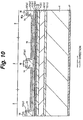
- Fig. 10 is a cross-sectional view for explaining the method of manufacturing the GaN compound semiconductor laser according to the first embodiment of the invention
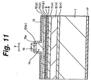
- Fig. 11 is a cross-sectional view for explaining the method of manufacturing the GaN compound semiconductor laser according to the first embodiment of the invention
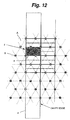
- Fig. 12 is a cross-sectional view for explaining a method of manufacturing a GaN compound semiconductor laser according to the second embodiment of the invention
- FIG. 13 is a schematic diagram showing an edge of a chip obtained by dicing in the method of manufacturing the GaN compound semiconductor laser according to the second embodiment of the invention
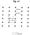
- Fig. 14 is a plan view for explaining a method of manufacturing a GaN compound semiconductor laser according to the third embodiment of the invention
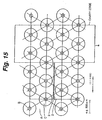
- Fig. 15 is a plan view for explaining a method of manufacturing a GaN compound semiconductor laser according to the fourth embodiment of the invention
- Fig. 16 is a plan view for explaining a method of manufacturing a GaN compound semiconductor laser according to the fifth embodiment of the invention
- Fig. 17 is a plan view for explaining a method of manufacturing a GaN compound semiconductor laser according to the sixth embodiment of the invention
- FIG. 18 is a plan view for explaining a method of manufacturing a GaN compound semiconductor laser according to the seventh embodiment of the invention
- Fig. 19 is a cross-sectional view showing the GaN compound semiconductor laser manufactured by the method according to seventh embodiment of the invention
- Fig. 20 is a plan view for explaining a method of manufacturing a GaN compound semiconductor laser according to the eighth embodiment of the invention
- Fig. 21 is a cross-sectional view showing the GaN semiconductor laser manufactured by the method according to eighth embodiment of the invention
- Fig. 22 is a plan view for explaining a method of manufacturing a GaN compound semiconductor laser according to the ninth embodiment of the invention
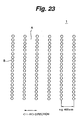
- Fig. 23 is a plan view for explaining a method of manufacturing a GaN compound semiconductor laser according to the tenth embodiment of the invention
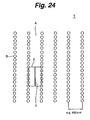
- Fig. 24 is a plan view for explaining a method of manufacturing a GaN compound semiconductor laser according to the tenth embodiment of the invention
- Fig. 25 is a plan view for explaining a method of manufacturing a GaN compound semiconductor laser according to the eleventh embodiment of the invention
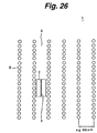
- Fig. 26 is a plan view for explaining a method of manufacturing a GaN compound semiconductor laser according to the twelfth embodiment of the invention
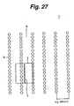
- Fig. 27 is a plan view for explaining a method of manufacturing a GaN compound semiconductor laser according to the thirteenth embodiment of the invention
- Fig. 28 is a plan view for explaining a method of manufacturing a GaN compound semiconductor laser according to the fourteenth embodiment of the invention
- FIG. 29 is a plan view for explaining a method of manufacturing a GaN compound semiconductor laser according to the fifteenth embodiment of the invention
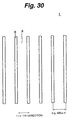
- Fig. 30 is a plan view for explaining a method of manufacturing a GaN compound semiconductor laser according to the sixteenth embodiment of the invention
- Fig. 31 is a plan view for explaining a method of manufacturing a GaN compound semiconductor laser according to the sixteenth embodiment of the invention
- Fig. 32 is a plan view for explaining a method of manufacturing a GaN compound semiconductor laser according to the seventeenth embodiment of the invention
- Fig. 33 is a plan view for explaining a method of manufacturing a GaN compound semiconductor laser according to the eighteenth embodiment of the invention
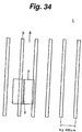
- Fig. 34 is a plan view for explaining a method of manufacturing a GaN compound semiconductor laser according to the nineteenth embodiment of the invention
- Fig. 35 is a plan view for explaining a method of manufacturing a GaN compound semiconductor laser according to the twentieth embodiment of the invention
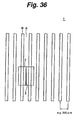
- Fig. 36 is a plan view for explaining a method of manufacturing a GaN compound semiconductor laser according to the twenty-first embodiment of the invention.
- Fig. 1A shows a cross-sectional view taken along a line where the regions B appear closest to each other.
- Fig. 1 shows them in form of circular cylinders for simplicity (also in the description hereunder).
- MOCVD metal-organic chemical vapor deposition
- HVPE halide vapor phase epitaxial growth
- each device region is defined in form of a rectangular shape of 400 ⁇ 346 ⁇ m.
- the value, 346 ⁇ m is equal to 400 ⁇ m ⁇ (3 1/2 /2).
- Each device region which is rectangular and sized 400 ⁇ 346 ⁇ m, is divided as a chip by dicing the substrate along the broken lines in Fig. 3, for example.
- the regions B are permitted to exist on end surfaces and corners of each semiconductor device.
- the device is a semiconductor laser
- its emission region is stripe-shaped in most cases.
- structure of the semiconductor laser is designed to ensure that the stripe does not lie on any of the regions B.
- Fig. 4 shows an example of such placement of the stripe.
- each device region can be defined in a location intentionally avoiding adverse affections by the regions B having more defects.
- the device is a semiconductor laser
- additional attention is paid to ensure that the cavity edges of its emission region does not lie on any of the regions B when the device region or device structure is designed.
- end surfaces of the chip serve as its cavity edges. Therefore, if the portion serving as the mirror of the cavity overlaps the regions B having lots of crystal defects as shown in Fig. 5, then the laser property will be lost. Therefore, position of the emission region and location of the device region on the substrate are determined when designed to ensure that the mirror portion of the cavity does not overlap the regions B.
- the rectangular shape sized 400 ⁇ 346 ⁇ m is one of examples, and any other sizes and shapes may be selected for devices to satisfy the conditions set forth in items (2) and (3).
- a GaN compound semiconductor laser is formed by growing GaN compound semiconductor layers on a GaN substrate in which regions B composed of a crystal having a high average dislocation density are regularly aligned in a region A composed of a crystal having a low average dislocation density.
- Fig. 6 is a plan view showing the GaN substrate used in the first embodiment. Perspective and cross-sectional views of the GaN substrate 1 appear as shown in Figs. 1A and 1B.
- the GaN substrate 1 is an n-type substrate having a (0001) plane (C-plane) orientation.
- the GaN substrate 1, however, may be of an R-plane, A-plane or M-plane orientation.
- regions B composed of a crystal having a high average dislocation density periodically align in form of hexagonal lattices in the region A having a low average dislocation density. In this case, the straight line connecting nearest two regions B coincides with the ⁇ 1-100> orientation of GaN or its equivalent.
- the straight line connecting nearest two regions B may coincide with the ⁇ 11-20> orientation or its equivalent of GaN.
- the regions B penetrate the GaN substrate 1. Thickness of the GaN substrate 1 is 200-600 ⁇ m, for example.
- Broken lines in Fig. 6 are shown only for demonstrating relative positional relations among the regions B, and they are not real (physically significant) lines (also in the description hereunder).
- the period of alignment of the regions B is 400 ⁇ m, and diameter of each region B is 20 ⁇ m, for example.
- Average dislocation density of the region A is 2 ⁇ 10 6 cm -2
- average dislocation density of the regions B is 1 ⁇ 10 8 cm -2 .
- Fig. 7 shows an example of distribution of the dislocation density of the regions B in radial directions of their centers.
- the GaN substrate 1 can be manufactured by using a crystal growth technique in the following manner, for example.
- Basic mechanism of crystal growth used for manufacturing the GaN substrate 1 is to grow it to have an oblique surface composed of facets and progress the growth while maintaining the oblique surface of facets so that dislocations propagate and concentrate to predetermined positions. Regions grown with facets become low-density defect regions due to movement of dislocations. In the lower portion of the oblique surface of facets, growth progresses to include high-density defect regions having clear boundaries. Dislocations concentrate onto boundaries with high-density defect regions or inside them, and disappear or accumulate there.
- facets exhibit different shapes.
- a defect region is dot-shaped, facets surrounds the dot as the bottom, and form a pit composed of facets.
- a defect region is stripe-shaped, oblique surfaces of facets are formed on opposite sides of the stripe as the valley bottom just like two facets of a laid-down triangular prism.
- the top surface of the growth layer is treated by cutting and polishing to flatten it.
- the GaN substrate 1 is ready for use as the substrate.
- the high-density defect regions may have some different states.
- they may be polycrystals.
- they may be monocrystals which, however, are slightly slanted with respect to low-density defect regions around them.
- their C-axes may be inverted with respect to low-density defect regions around them. In this fashion, the high-density defect regions have clear boundaries and are distinguished from their surround.
- the high-density defect regions can be generated by forming seeds beforehand at positions where the high-density defect regions should be formed by crystal growth of GaN on a base substrate. As these seeds, an amorphous or polycrystalline layers are formed. Thus, by growing GaN thereon, high-density defect regions can be formed just in the regions of the seeds.
- a base substrate is prepared.
- the base substrate may be selected from various kinds of substrates. It may be a typically sapphire substrate. However, for removal in a later process, a GaAs substrate easy to remove is preferably used.
- the seeds may be dot-shaped or stripe-shaped, for example. A desired number of seeds can be formed in regular alignment. More specifically, the seeds are formed in alignment corresponding to the alignment of the regions B shown in Fig. 6 in this case.
- GaN is grown thick by hydride vapor-phase epitaxy (HVPE), for example.
- HVPE hydride vapor-phase epitaxy
- facets corresponding to the pattern of the seeds appear on the surface of the thick layer of GaN obtained by the growth.
- the seeds have a pattern of dots, pits made by facets are regularly formed.
- the seeds exhibit a pattern of stripes, facets just like those of prisms appear.
- the base substrate is removed, and the top surface of the GaN thick layer is flattened by cutting and polishing. As a result, the GaN substrate 1 is obtained. Thickness of the GaN substrate 1 may be determined as desired.
- the GaN substrate 1 manufactured as explained above has a C-plane as its major surface, and includes therein dot-shaped (or stripe-shaped) high-density defect regions, i.e. Regions B, of a predetermined size, which are aligned regularly.
- the single-crystal region, i.e. the region A, which is the remainder part excluding the regions B, has a lower dislocation density than the regions B.
- device regions 2 of the illustrated geometry are defined on the GaN substrate 1 shown in Fig. 1 in the location shown in Fig. 7.
- GaN compound semiconductor layers composing laser structures are grown on the GaN substrate 1, and through steps of forming laser stripes and as well as other necessary steps, laser structures are formed.
- the GaN substrate 1 having the laser structures thereon is divided to discrete GaN compound semiconductor laser chips by dicing the substrate along the border lines of individual device regions 2.
- the dark rectangle corresponds to a single GaN compound semiconductor laser, and the straight line passing its central part shows the laser stripe 3 that corresponds to the position of the emission region.
- the rectangle bounded by the solid lines and broken lines and broken lines continuous therefrom correspond to a laser bar 4, and the longer sides of the laser bar 4 correspond to cavity edges.
- the GaN compound semiconductor laser is sized 600 ⁇ 346 ⁇ m, for example.
- the substrate is divided to discrete GaN compound semiconductor lasers of this size by dicing the substrate along straight lines connecting regions B in the horizontal direction (lengthwise directions of the lasers) and long straight lines not passing regions B in the vertical direction (parallel to the shorter sides of the lasers).
- regions B can reside only on side surfaces of longer sides of each GaN compound semiconductor laser. Therefore, by designing the devices such that their laser stripes 3 each extend near the straight line of midpoints of the shorter sides, Influences of the regions B to the emission regions can be prevented.
- Cavity mirrors are formed on edges by dicing the substrate by cleavage, or the like, along the vertical straight lines in Fig. 8. Since these straight lines do not pass any of the regions B, the cavity mirrors are not affected by dislocations in the regions B. Therefore, GaN compound semiconductor lasers excellent in emission property and enhanced in reliability can be obtained.
- the GaN compound semiconductor laser has a ridge structure and a SCH structure (separate confinement heterostructure).
- the top surface of the GaN substrate 1 is cleaned by thermal cleaning, for example.
- the n-type GaN buffer layer 5 is 0.05 ⁇ m thick, for example, and it is doped with Si, for example, as its n-type impurity.
- the n-type AlGaN clad layer 7 is 1.0 ⁇ m thick, and it is doped with Si, for example, as its impurity. Its Al composition may be 0.08, for example.
- the n-type GaN optical guide layer 7 is 0.1 ⁇ m thick, for example, and it is doped with Si, for example, as its n-type impurity.
- the active layer 8 includes three well layers.
- the undoped InGaN deterioration preventive layer 9 has a graded structure in which the In composition gradually, monotonously decreases from the surface in contact with the active layer 8 toward the surface in contact with the p-type AlGaN cap layer 9.
- the surface in contact with the active layer 8 is equal in In composition to the In composition y of the In y Ga 1-y N layer as the barrier layer of the active layer 8.
- In composition of the surface in contact with the p-type AlGaN cap layer 10 is zero.
- Thickness of the undoped InGaN deterioration preventive layer 9 may be 20 nm, for example.
- the p-type AlGaN cap layer 10 is 10 nm thick, for example, and it is doped with magnesium (Mg), for example, as its p-type impurity.
- Al composition of the p-type AlGaN cap layer 10 is 0.2, for example.
- the p-type AlGaN cap layer 10 functions not only to prevent deterioration of the active layer 8 by elimination of In during growth of the p-type GaN optical guide layer 11 and the p-type AlGaN cap layer 11 but also to prevent overflow of carriers (electrons) from the active layer.
- the p-type GaN optical guide layer is 0.1 ⁇ m thick, for example, and it is doped with Mg, for example, as its p-type impurity.
- the p-type AlGaN clad layer 12 is 0.5 ⁇ m thick, for example, and it is doped with Mg, for example, as its p-type impurity. Al composition of the layer 12 may be 0.08, for example.
- the p-type GaN contact layer 13 is 0.1 ⁇ m thick, for example.
- the growth temperature may be around 1000°C, for example.
- the growth temperature may be 700-800°C. For example, it may be 730°C.
- the growth temperature is adjusted to 730°C, for example, equally to the growth temperature of the active layer 8 at the start of its growth, and it is thereafter increased linearly, for example, to reach 835°C equal to the growth temperature of the p-type AlGaN cap layer 10 at the end of its growth.
- Source materials for growth of these GaN compound semiconductor layers may be, for example, trimethyl gallium ((CH 3 ) 3 Ga, TMG) as the material of Ga, trimethyl aluminum ((CH 3 ) 3 Al, TMA) as the material of Al, trimethyl indium ((CH 3 ) 3 In, TMI) as the material of In and NH 3 as the material of N.
- the carrier gas may be H 2 , for example.
- the c-plane sapphire substrate having those GaN compound semiconductor layers grown thereon as explained above is removed from the MOCVD apparatus.
- a SiO 2 film (not shown), 0.1 ⁇ m thick for example, is formed on the entire surface of the p-type GaN contact layer 13 by CVD, vacuum evaporation or sputtering, for example, a resist pattern (not shown) of a predetermined configuration corresponding to the shape of the ridge portion is formed on the SiO 2 film by lithography.
- the SiO 2 film is selectively etched to a pattern corresponding to the ridge portion by wet etching using a hydrofluoric acid-based etching liquid, or RIE using an etching gas containing fluorine such as CF 4 or CHF 3 .
- the underlying layers are selectively etched by RIE, for example, down to a predetermined depth of the p-type AlGaN clad layer 12 to obtain the ridge 14 extending in the ⁇ 1-100> direction as shown in Fig. 10.
- the ridge 14 is 3 ⁇ m wide, for example.
- a chlorine-based is be used as the etching gas, for example.
- an insulating film 15 such as a 0.3 ⁇ m thick SiO 2 film, for example, is formed on the entire surface of the substrate by CVD, vacuum evaporation or sputtering, for example.
- the insulating film 15 serves as an electrical insulator and a surface protector.
- a resist pattern (not shown) locally covering the insulating film 15 excluding the region for a p-side electrode is formed by lithography.
- the insulating film 15 is etched to form an opening 15a.
- a Pd film, Pt film and Au film are sequentially deposited on the entire substrate surface by vapor deposition, for example, and the resist pattern is removed together with the overlying Pd film, Pt film and Au film (lift-off).
- the p-side electrode 16 in contact with the p-type GaN contact layer 13 through the opening 15a of the insulating film 15 is obtained.
- the Pd film, Pt film and Au film composing the p-side electrode 16 are 10 nm, 100 nm and 300 nm thick, respectively, for example. Thereafter, alloying is carried out to bring the p-side electrode 16 into ohmic contact.
- a Ti film, Pt film and Au film are sequentially deposited on the bottom surface of the GaN substrate 1 by vacuum evaporation, for example, to form the n-side electrode having a Ti/Pt/Au structure.
- the Ti film, Pt film and Au film composing the n-side electrode 17 are 10 nm, 50 nm and 100 nm thick, respectively, for example. Thereafter, alloying is carried out to bring the n-side electrode 17 into ohmic contact.
- the GaN substrate 1 having formed the laser structures through the foregoing steps is cut into laser bars by dicing it by cleavage along the border lines of the device regions 2 to form opposite cavity edges. Further, after coating these cavity edges, each bar is divided to chips by dicing it by cleavage, or the like.
- the intended GaN compound semiconductor lasers having the ridge structure and the SCH structure are completed as shown in Fig. 11.
- each device region 2 is defined on the GaN substrate 1 which includes the regions B having a higher average dislocation density and aligned periodically in form of hexagonal lattices in the region A having a lower average dislocation density such that each device region 2 includes substantially no region B, and the GaN compound semiconductor layers, which will form laser structures, are grown on the GaN substrate 1. Therefore, even when some defects, such as dislocations, propagate from the regions B of the GaN compound semiconductor layer 1, the GaN compound semiconductor layers on the device regions 2 can be held free from influences of those defects.
- the GaN substrate 1 having formed the laser structures is divided into discrete GaN compound semiconductor laser chips by dicing it along the border lines of the device regions 2. Therefore, any of the GaN compound semiconductor laser chips include substantially no dislocations taken over from the GaN substrate 1. As a result, GaN compound semiconductor lasers excellent in emission property, enhanced in reliability and elongated in lifetime can be realized.
- the undoped InGaN deterioration preventive layer 9 is formed in contact with the active layer 8, and the p-type AlGaN cap layer 10 is formed in contact with the undoped InGaN deterioration preventive layer 9. Therefore, the undoped InGaN deterioration preventive layer 9 greatly alleviates the stress exerted from the p-type AlGaN cap layer 10 to the active layer 8. At the same time, dispersion of Mg used as a p-type dopant of p-type layers into the active layer 7 is prevented effectively.
- both the shorter sides and the longer sides of the rectangular device region 2, which form border lines of each device region 2 are straight lines connecting centers of regions B unlike the first embodiment.
- the laser stripes 3 lie on lines connecting midpoints of shorter sides of individual device regions 2. In this manner, transfer of influence of the regions B to the emission regions can be prevented.
- the second embodiment is different from the first embodiment in forming cavity mirrors by dicing the substrate by cleavage along the border lines of the device regions 2 that are straight lines connecting centers of regions B.
- the regions B having more dislocations are considered easier to break than the region A. Therefore, when the substrate is diced along the straight lines that connect regions B, the regions B function as perforation, and the region A is clearly cleaved, too. In this case, regions B appearing on edges have many dislocations, and will not always become smooth. However, the region A appearing between the regions B on the edges becomes smooth. Such a configuration of an edge is schematically shown in Fig. 13.
- the second embodiment ensures the same advantages as those of the first embodiment.
- regions B made of a crystal having a higher average dislocation density are aligned periodically in form of rectangular lattices in the region A having a lower average dislocation density in a GaN substrate 1.
- a single rectangle having regions B at its four corners is defined as a single device region 2.
- each straight line connecting nearest two adjacent regions B in the lengthwise direction of the rectangle coincides with the ⁇ 1-100> orientation of GaN
- each straight line connecting nearest two adjacent regions B and being one of shorter side of the rectangle coincides with the ⁇ 11-20> orientation of GaN.
- Interval of regions B in the lengthwise direction of the rectangular lattices is 600 ⁇ m, for example, and interval of regions B in the direction parallel to the shorter sides of the rectangular lattices is 400 ⁇ m, for example.
- each device region 2 is sized 600 ⁇ 400 ⁇ m.
- the laser stripe 3 of each device region 2 lies on the straight line connecting midpoints of opposite shorter sides.
- the third embodiment also ensures the same advantages as those of the first embodiment.
- regions B are aligned periodically in form of hexagonal lattices in the region A of the GaN substrate 1 similarly to the first embodiment.
- the fourth embodiment is different from the first embodiment in including regions C having an intermediate average dislocation density between the average dislocation density of the region A and the average dislocation density of the regions B and interposed between the region A and individual regions B. More specifically, the average dislocation density of the region A is 2 ⁇ 10 6 cm -2 or more, the average dislocation density of the regions B is 1 ⁇ 10 8 cm -2 or more, and the average dislocation density of the regions C is smaller than 1 ⁇ 10 8 cm -2 and larger than 2 ⁇ 10 6 cm -2 .
- Interval of the regions B (distance between the centers of nearest two adjacent regions B) is 300 ⁇ m, for example, diameter of each region B is 20 ⁇ m. Diameter of each region C is 120 ⁇ m, for example.
- both the longer sides and the shorter sides of each rectangular device region 2, which define border lines thereof, are straight lines that connect centers of regions B.
- Each device region is sized 600 ⁇ 260 ⁇ m of each rectangular device region 2.
- the laser stripes 3 lie on lines connecting midpoints of shorter sides of individual device regions 2. In this embodiment, however, the laser stripes 3 overlap no regions B and no regions C. In this manner, transfer of influence of the regions B and C to the emission regions can be prevented.
- the fourth embodiment also ensures the same advantages as those of the first embodiment.
- regions B are aligned periodically in form of hexagonal lattices in the region A of the GaN substrate 1 similarly to the first embodiment.
- the fifth embodiment is different from the first embodiment in including regions C having an intermediate average dislocation density between the average dislocation density of the region A and the average dislocation density of the regions B and interposed between the region A and individual regions B. More specifically, the average dislocation density of the region A is 2 ⁇ 10 6 cm -2 or more, the average dislocation density of the regions B is 1 ⁇ 10 8 cm -2 or more, and the average dislocation density of the regions C is smaller than 1 ⁇ 10 8 cm -2 and larger than 2 ⁇ 10 6 cm -2 .
- Interval of the regions B (distance between the centers of nearest two adjacent regions B) is 400 ⁇ m, for example, diameter of each region B is 20 ⁇ m. Diameter of each region C is 120 ⁇ m, for example.
- the device region 2 taken as the first example is defined such that the border lines corresponding to the shorter sides of the rectangular device region 2 are straight lines connecting centers of regions B and the border lines corresponding to the longer sides of the rectangle are straight lines distant by 23 ⁇ m from straight lines connecting nearest adjacent two regions B.
- the device region 2 is sized 400 ⁇ 300 ⁇ m, for example.
- the laser stripes 3 lie on lines connecting midpoints of shorter sides of individual device regions 2. In this embodiment, however, the laser stripes 3 overlap no regions B and no regions C. In this manner, transfer of influence of the regions B and C to the emission regions can be prevented.
- the device region 2 taken as the second example is defined such that the border lines corresponding to the longer sides of the rectangular device region 2 are distant by 23 ⁇ m from straight lines connecting centers of nearest two adjacent regions B in the ⁇ 1-100> direction, and the border lines corresponding to the shorter sides of the rectangle are distant by 100 ⁇ m from straight lines connecting nearest two adjacent regions B in the ⁇ 11-20> direction.
- the device region 2 is sized 400 ⁇ 300 ⁇ m, for example, and the laser stripes 3 lie on lines connecting midpoints of shorter sides of individual device regions 2. In this embodiment, however, the laser stripes 3 overlap no regions B and no regions C. In this manner, transfer of influence of the regions B and C to the emission regions can be prevented.
- the fifth embodiment also ensures the same advantages as those of the first embodiment.
- regions B are aligned periodically in form of hexagonal lattices in the region A of the GaN substrate 1 similarly to the first embodiment.
- the sixth embodiment is different from the first embodiment in that the span between centers of closest adjacent regions B in the ⁇ 1-100> direction is two times the length of a shorter side of each rectangular device region 2, i.e. 700 ⁇ m, for example.
- Border lines defining shorter sides of each device region 2 lie on straight lines each connecting closest adjacent regions B in the ⁇ 11-20> direction whereas border lines defining the longer sides lie on straight lines each connecting closest adjacent regions B in the ⁇ 1-100> direction.
- each device region 2 is sized 606 ⁇ 350 ⁇ m, for example.
- the laser stripes 3 lie on lines connecting midpoints of shorter sides of individual device regions 2, do not overlap any of the regions B. In this manner, transfer of influence of the regions B to the emission regions can be prevented.
- the sixth embodiment also ensures the same advantages as those of the first embodiment.
- Fig. 19 shows a GaN compound semiconductor laser chip obtained by dicing along border lines of device regions 2.
- the seventh embodiment also ensures the same advantages as those of the first embodiment in a multibeam GaN compound semiconductor laser.
- a laser stripe 3 is formed in each device region similarly to the first embodiment.
- the laser stripe 3 is much wider than that of the first embodiment. More specifically, when the length of the shorter side of each rectangular device region 2 is a and the diameter of each region B is d, the maximum width of each laser stripe 3 will be a-d. However, the laser stripe 3 had better be apart from regions B by at least 1 ⁇ m. Taking it into account, the practical maximum width of the laser stripe 3 will be a-d-2 ⁇ m.
- the laser stripe 3 may be 200 ⁇ m wide.
- Fig. 21 shows a GaN compound semiconductor laser chip obtained by dicing along borderlines of device regions 2 in that example.
- the eighth embodiment also ensures the same advantages as those of the first embodiment.
- Fig. 22 is a plan view showing a GaN substrate used in the ninth embodiment.
- device regions B are defined not include regions B in laser stripes 3.
- the laser stripes 3 are distant from regions B by at least 50 ⁇ m.
- the device 2 illustrated here results in overlapping two regions B.
- the ninth embodiment also ensures the same advantages as those of the first embodiment.
- Fig. 23 is a plan view showing a GaN substrate used in the tenth embodiment.
- This GaN substrate 1 is an n-type substrate having the C-plane orientation.
- the GaN substrate may have the R-plane, A-plane or M-plane orientation, alternatively.
- regions B composed of a crystal having a higher average dislocation density are aligned in the region A composed of a crystal having a lower average dislocation density in periodical intervals of 400 ⁇ m, for example, in the ⁇ 11-20> direction and in periodical intervals of 20 ⁇ 100 ⁇ m, for example in the ⁇ 1-100> direction normal to the ⁇ 11-20> direction.
- the ⁇ 11-20> and ⁇ 1-100> directions may be vice versa.
- device regions 2 are defined such that a pair of end surfaces parallel to the laser stripes 3 lie on neighboring rows of regions B in the ⁇ 1-100> direction, respectively, and the laser stripe 3 lies near the center of the region between those rows of the regions B. In this case, any of the device regions 2 does not substantially include any row of regions B.
- the tenth embodiment also ensures the same advantages as those of the first embodiment.
- the eleventh embodiment uses a GaN substrate 1 similar to that of the tenth embodiment. However, it is different from the tenth embodiment in that one end surface parallel to each laser stripe lies on a row of regions B in the ⁇ 1-100> direction but the opposite end surface extend along a line distant from a next row of regions B.
- any of the device regions 2 does not substantially include any row of regions B.
- the eleventh embodiment also ensures the same advantages as those of the first embodiment.
- the twelfth embodiment uses a GaN substrate 1 similar to that of the tenth embodiment. However, it is different from the tenth embodiment in that the device regions 2 are defined such that both of opposite end surfaces parallel to the laser stripe 3 reside between neighboring rows of regions B in the ⁇ 1-100> direction and the laser stripe 3 resides near the center in the area between those rows of regions B.
- any of the device regions 2 does not substantially include any row of regions B.
- the twelfth embodiment also ensures the same advantages as those of the first embodiment. Therefore, their explanation is omitted.
- the thirteenth embodiment uses a GaN substrate 1 similar to that of the tenth embodiment. However, it is different from the tenth embodiment in that one of pair of end surfaces parallel to the laser stripe 3 lies on a row of regions B in the ⁇ 1-100> direction whereas the other end surface resides between next two rows of regions B and the laser stripe 3 extends along a line distant from the nearest row of regions B by 50 ⁇ m or more. In this case, each device region 2 includes one row of regions B.
- the thirteenth embodiment also ensures the same advantages as those of the first embodiment.
- the fourteenth embodiment uses a GaN substrate 1 similar to that of the tenth embodiment. However, it is different from the tenth embodiment in that one of end surfaces parallel to the laser stripe 3 extends along a line distant from a row of regions B in the ⁇ 1-100> direction whereas the other end surface extends between next two rows of regions B, and that the laser stripe 3 extends along a line distant from the nearest row of regions B by 50 ⁇ m or more. In this case, each device region 2 includes one row of regions B.
- the fourteenth embodiment also ensures the same advantages as those of the first embodiment.
- Fig. 29 is a plan view showing a GaN substrate 1 used in the fifteenth embodiment.
- each laser stripe 3 extends near the center of the area between neighboring rows of regions B, and a pair of end surfaces parallel to the laser stripe 3 extends near the center of the area between the former rows of regions B and rows of regions B outwardly next to them.
- the fifteenth embodiment also ensures the same advantages as those of the first embodiment.
- Fig. 30 is a plan view showing a GaN substrate 1 used in the sixteenth embodiment.
- This GaN substrate 1 is an n-type substrate and having the C-plane orientation.
- the GaN substrate 1, however, may be of an R-plane, A-plane or M-plane orientation.
- regions B composed of a crystal having a high average dislocation density and linearly extending in the ⁇ 1-100> direction are periodically align in intervals of 400 ⁇ m, for example, in the ⁇ 11-20> direction normal to the ⁇ 1-100> direction.
- the ⁇ 11-20> and ⁇ 1-100> directions may be vice versa.
- device regions 2 are defined such that a pair of end surfaces parallel to each laser stripe 3 lie on regions B and the laser stripe 3 resides near the center of the area between these regions B. In this case, any of the device regions 2 includes substantially no region B.
- the sixteenth embodiment also ensures the same advantages as those of the first embodiment.
- the seventeenth embodiment uses a GaN substrate 1 similar to that of the sixteenth embodiment. However, it is different from the sixteenth embodiment in that one of end surfaces parallel to each laser stripe 3 lies on one of regions B whereas the other end surface extends along a line distant from any of the linear regions B.
- any of the device regions 2 includes substantially no linear region B.
- the seventeenth embodiment also ensures the same advantages as those of the first embodiment.
- the eighteenth embodiment uses a GaN substrate 1 similar to that of the sixteenth embodiment. However, it is different from the sixteenth embodiment in that the device regions 2 are defined such that both of the opposite end surfaces parallel to each laser stripe 3 extend in the area between neighboring regions B and the laser stripe 3 extends near the center of the area between those regions B.
- any of the device regions 2 includes substantially no linear region B.
- the eighteenth embodiment also ensures the same advantages as those of the first embodiment.
- the eighteenth embodiment uses a GaN substrate 1 similar to that of the sixteenth embodiment. However, it is different from the sixteenth embodiment in that one of end surfaces parallel to each laser stripe 3 lies on one of regions B whereas the opposite end surface extend in the area between next two regions B and that the laser stripe 3 extends along a line distant from nearest one of regions B by at least 50 ⁇ m.
- each device region 2 includes one region B.
- the nineteenth embodiment also ensures the same advantages as those of the first embodiment.
- the twentieth embodiment uses a GaN substrate 1 similar to that of the sixteenth embodiment. However, it is different from the sixteenth embodiment in that one of end surfaces parallel to each laser stripe 3 extends along a line distant from nearest one of regions B whereas the opposite end surface extend in the area between next two regions B and that the laser stripe 3 extends along a line distant from nearest one of regions B by at least 50 ⁇ m.
- each device region 2 includes one region B.
- the twentieth embodiment also ensures the same advantages as those of the first embodiment.
- Fig. 36 is a plan view of a GaN substrate 1 used in the twenty-first embodiment.
- the GaN substrate 1 is identical to the GaN substrate used in the sixteenth embodiment except that the regions B periodically align in the ⁇ 11-20> direction of GaN in intervals of 200 ⁇ m, for example.
- each device region 2 includes two linear regions B.
- each laser stripe 3 resides near the center of the area between neighboring regions B, and a pair of end surfaces parallel to the laser stripe 3 extend in areas between those regions B and their outwardly neighboring regions B, respectively.
- the twenty-first embodiment also ensures the same advantages as those of the first embodiment.
- those embodiments have been explained as first depositing n-type layers as components of laser structures on the substrate and thereafter depositing p-type layers.
- the order of depositing layers may be inverted to deposit p-type layers first on the substrate and deposit n-type layers thereon.
- GaN compound semiconductor lasers of SCH structures have been explained as being applied to the manufacture of GaN compound semiconductor lasers of SCH structures.
- the present invention is of course applicable to GaN compound semiconductor lasers of DH structures (double heterostructures), for example, and applicable to the manufacture of GaN compound light emitting diodes.
- the invention is applicable to electron transport devices using nitride III-V compound semiconductors, such as GaN compound FETs and GaN heterojunction bipolar transistors (HBTs).
- H 2 gas as the carrier gas for growth by MOCVD.
- any other appropriate carrier gas such as a mixed gas of H 2 with N 2 or with He, Ar gas, or the like.
- cavity edges may be formed by dry etching such as RIE.
- device regions are defined on the nitride III-V compound semiconductor substrate, other semiconductor substrate or any kind of substrate such that active regions of devices do not substantially include the second regions higher in average dislocation density, higher in average defect density or inferior in crystalline property to the first region. Therefore, even if dislocations or other defects propagate from the second regions to nitride III-V compound semiconductor layers, other semiconductor layers, or layers of any other various kinds of materials, which are deposited for forming light emitting device structures or other device structures, it is ensured that chips obtained by dicing the substrate include substantially no dislocations or other defects.
- the invention can realize semiconductor light emitting devices excellent in emission property, enhanced in reliability and elongated in lifetime, or other semiconductor devices excellent in property, enhanced in reliability and elongated in lifetime, or other various kinds of devices excellent in property, enhanced in reliability and elongated in lifetime.
Landscapes
- Chemical & Material Sciences (AREA)
- Physics & Mathematics (AREA)
- Engineering & Computer Science (AREA)
- Crystallography & Structural Chemistry (AREA)
- Optics & Photonics (AREA)
- Materials Engineering (AREA)
- Metallurgy (AREA)
- Organic Chemistry (AREA)
- Electromagnetism (AREA)
- Condensed Matter Physics & Semiconductors (AREA)
- General Physics & Mathematics (AREA)
- Inorganic Chemistry (AREA)
- Nanotechnology (AREA)
- General Chemical & Material Sciences (AREA)
- Chemical Kinetics & Catalysis (AREA)
- Life Sciences & Earth Sciences (AREA)
- Biophysics (AREA)
- Semiconductor Lasers (AREA)
- Led Devices (AREA)
Abstract
Description
(1) When the device is designed, its size is determined in accord with the period of alignment of the regions B.
(2) Location of each device region is determined to ensure that the device region does not lie on any of the regions B substantially, that is, to ensure that the device region includes substantially no region B.
(3) When the device is designed, position of the active region inside the device is determined not to lie on any of the regions B.
Therefore, their explanation is omitted.
Claims (129)
- A method of manufacturing a semiconductor light emitting device by growing nitride III-V compound semiconductor layers forming a light emitting device structure on a nitride III-V compound semiconductor substrate in which a plurality of second regions having a second average dislocation density higher than a first average dislocation density align regularly in a first region made of a crystal and having the first average dislocation density, comprising:defining a device region on the nitride III-V compound semiconductor substrate such that the device region does not include the second regions substantially.
- The method of manufacturing a semiconductor light emitting device according to claim 1 wherein the device region is determined in size and location such that the device region does not include the second regions substantially.
- The method of manufacturing a semiconductor light emitting device according to claim 1 wherein the second regions align periodically.
- The method of manufacturing a semiconductor light emitting device according to claim 1 wherein the second regions align periodically in form of hexagonal lattices.
- The method of manufacturing a semiconductor light emitting device according to claim 1 wherein the second regions align periodically in form of rectangular lattices.
- The method of manufacturing a semiconductor light emitting device according to claim 1 wherein the second regions align periodically in form of square lattices.
- The method of manufacturing a semiconductor light emitting device according to claim 1 wherein the device region is rectangular.
- The method of manufacturing a semiconductor light emitting device according to claim 7 wherein a pair of opposed sides of the device region are parallel to the <1-100> direction, and the other pair of opposed sides are parallel to the <11-20> direction.
- The method of manufacturing a semiconductor light emitting device according to claim 1 wherein the device region is square.
- The method of manufacturing a semiconductor light emitting device according to claim 1 wherein the interval between neighboring two of the second regions is 20 µm or more.
- The method of manufacturing a semiconductor light emitting device according to claim 1 wherein the interval between neighboring two of the second regions is 50 µm or more.
- The method of manufacturing a semiconductor light emitting device according to claim 1 wherein the interval of neighboring two of the second regions is 100 µm or more.
- The method of manufacturing a semiconductor light emitting device according to claim 3 wherein the period of alignment of the second regions is 20 µm or more.
- The method of manufacturing a semiconductor light emitting device according to claim 3 wherein the period of alignment of the second regions is 50 µm or more.
- The method of manufacturing a semiconductor light emitting device according to claim 3 wherein the period of alignment of the second regions is 100 µm or more.
- The method of manufacturing a semiconductor light emitting device according to claim 1 wherein the second regions penetrate the nitride III-V compound semiconductor substrate.
- The method of manufacturing a semiconductor light emitting device according to claim 1 wherein each said second region has an arbitrary polygonal prismatic shape.
- The method of manufacturing a semiconductor light emitting device according to claim 1 wherein third regions having a third average dislocation density higher than the first average dislocation density and lower than the second average dislocation density are interposed between the first region and the second regions.
- The method of manufacturing a semiconductor light emitting device according to claim 18 wherein the device region is defined such that the device region does not include the second regions and the third regions substantially.
- The method of manufacturing a semiconductor light emitting device according to claim 1 wherein each said second region has a diameter from 10 to 100 µm.
- The method of manufacturing a semiconductor light emitting device according to claim 1 wherein each said second region has a diameter from 20 to 50 µm.
- The method of manufacturing a semiconductor light emitting device according to claim 18 wherein each said third region has a diameter larger than the diameter of each said second region by a value from 20 to 200 µm.
- The method of manufacturing a semiconductor light emitting device according to claim 18 wherein each said third region has a diameter larger than the diameter of each said second region by a value from 40 to 160 µm.
- The method of manufacturing a semiconductor light emitting device according to claim 18 wherein each said third region has a diameter larger than the diameter of each said second region by a value from 60 to 140 µm.
- The method of manufacturing a semiconductor light emitting device according to claim 1 wherein the average dislocation density of the second regions is five times or more.
- The method of manufacturing a semiconductor light emitting device according to claim 1 wherein the average dislocation density of the second regions is 1×108cm-2 or more.
- The method of manufacturing a semiconductor light emitting device according to claim 1 wherein the average dislocation density of the first region is 2×106cm-2 or less, and the average dislocation density of the second regions is 1×108cm-2 or more.
- The method of manufacturing a semiconductor light emitting device according to claim 18 wherein the average dislocation density of the first region is 2×106cm-2 or less, the average dislocation density of the second regions is 1×108cm-2 or more, and the average dislocation density of the third regions is lower than 1×108cm-2 and higher than 2×106cm-2.
- The method of manufacturing a semiconductor light emitting device according to claim 1 wherein the emission region of the semiconductor light emitting device is distant from the second regions by at least 1 µm.
- The method of manufacturing a semiconductor light emitting device according to claim 1 wherein the emission region of the semiconductor light emitting device is distant from the second regions by at least 10 µm.
- The method of manufacturing a semiconductor light emitting device according to claim 1 wherein the emission region of the semiconductor light emitting device is distant from the second regions by at least 100 µm.
- The method of manufacturing a semiconductor light emitting device according to claim 18 wherein the emission region of the semiconductor light emitting device does not include the second regions and the third regions.
- The method of manufacturing a semiconductor light emitting device according to claim 1 wherein a region supplied with a drive current through a stripe-shaped electrode in the semiconductor light emitting device is distant from the second regions by at least 1 µm.
- The method of manufacturing a semiconductor light emitting device according to claim 1 wherein a region supplied with a drive current through a stripe-shaped electrode in the semiconductor light emitting device is distant from the second regions by at least 10 µm.
- The method of manufacturing a semiconductor light emitting device according to claim 1 wherein a region supplied with a drive current through a stripe-shaped electrode in the semiconductor light emitting device is distant from the second regions by at least 100 µm.
- The method of manufacturing a semiconductor light emitting device according to claim 18 wherein a region supplied with a drive current through a stripe-shaped electrode in the semiconductor light emitting device does not include the second regions and the third regions.
- The method of manufacturing a semiconductor light emitting device according to claim 1 wherein border lines of the device region includes a straight line connecting at least neighboring two of said second regions.
- The method of manufacturing a semiconductor light emitting device according to claim 1 wherein the nitride III-V compound semiconductor substrate having the nitride III-V compound semiconductor layers grown thereon is diced along border lines including at least neighboring two of the second regions.
- The method of manufacturing a semiconductor light emitting device according to claim 38 wherein the dicing is carried out by cleavage.
- The method of manufacturing a semiconductor light emitting device according to claim 1 wherein border lines of the device region are distant from the second regions by at least 1 µm.
- The method of manufacturing a semiconductor light emitting device according to claim 1 wherein the nitride III-V compound semiconductor substrate having the nitride III-V compound semiconductor layers grown thereon is diced along border lines distant from the second regions by at least 1 µm.
- The method of manufacturing a semiconductor light emitting device according to claim 41 wherein the dicing is carried out by cleavage.
- The method of manufacturing a semiconductor light emitting device according to claim 1 wherein the nitride III-V compound semiconductor substrate is made of AlxByGa1-x-y-zInzAsuN1-u-vPv (where 0≤x≤1, 0≤y≤1, 0≤z≤1, 0≤u≤1, 0≤v≤1, 0≤x+y+z<1 and 0≤u+v<1).
- The method of manufacturing a semiconductor light emitting device according to claim 1 wherein the nitride III-V compound semiconductor substrate is made of AlxByGa1-x-y-zInzN (where 0≤x≤1, 0≤y≤1, 0≤z≤1 and 0≤x+y+z<1).
- The method of manufacturing a semiconductor light emitting device according to claim 1 wherein the nitride III-V compound semiconductor substrate is made of AlxGa1-x-zInzN (where 0≤x≤1 and 0≤z≤1).
- The method of manufacturing a semiconductor light emitting device according to claim 1 wherein the nitride III-V compound semiconductor substrate is made of GaN.
- The method of manufacturing a semiconductor light emitting device according to claim 1 wherein the semiconductor light emitting device is a semiconductor laser.
- The method of manufacturing a semiconductor light emitting device according to claim 1 wherein the semiconductor light emitting device is a light emitting diode.
- A semiconductor light emitting device manufactured by:growing nitride III-V compound semiconductor layers forming a light emitting device structure on a nitride III-V compound semiconductor substrate in which a plurality of second regions having a second average dislocation density higher than a first average dislocation density align regularly in a first region made of a crystal and having the first average dislocation density; anddicing the nitride III-V compound semiconductor substrate having the nitride III-V compound semiconductor layers grown thereon along border lines including at least neighboring two of the second regions.
- A semiconductor light emitting device including nitride III-V compound semiconductor layers grown to form a light emitting device structure on a nitride III-V compound substrate in which a plurality of second regions having a second average dislocation density higher than a first average dislocation density align regularly in a first region made of a crystal and having the first average dislocation density, in which at least one of said second regions resides on an end surface or a corner of the nitride III-V compound semiconductor substrate.
- A method of manufacturing a semiconductor light emitting device by growing nitride III-V compound semiconductor layers forming a light emitting device structure on a nitride III-V compound semiconductor substrate in which a plurality of second regions having a second average defect density higher than a first average defect density align regularly in a first region made of a crystal and having the first average defect density, comprising:defining a device region on the nitride III-V compound semiconductor substrate such that the device region does not include the second regions substantially.
- A semiconductor light emitting device manufactured by:growing nitride III-V compound semiconductor layers forming a light emitting device structure on a nitride III-V compound semiconductor substrate in which a plurality of second regions having a second average defect density higher than a first average defect density align regularly in a first region made of a crystal and having the first average defect density; anddicing the nitride III-V compound semiconductor substrate having the nitride III-V compound semiconductor layers grown thereon along border lines including at least neighboring two of the second regions.
- A semiconductor light emitting device including nitride III-V compound semiconductor layers grown to form a light emitting device structure on a nitride III-V compound semiconductor substrate in which a plurality of second regions having a second average defect density higher than a first average defect density align regularly in a first region made of a crystal and having the first average defect density, in which at least one of said second regions resides on an end surface or a corner of the nitride III-V compound semiconductor substrate.
- A method of manufacturing a semiconductor light emitting device by growing nitride III-V compound semiconductor layers forming a light emitting device structure on a nitride III-V compound semiconductor substrate in which a plurality of second regions inferior in crystalline property to a first region align regularly in the first region made of a crystal, comprising:defining a device region on the nitride III-V compound semiconductor substrate such that the device region does not include the second regions substantially.
- The method of manufacturing a semiconductor light emitting device according to claim 54 wherein the first region is a single crystal, and the second regions are composed of a single crystal, a polycrystal, amorphous substance, or their mixture.
- A semiconductor light emitting device manufactured by:growing nitride III-V compound semiconductor layers forming a light emitting device structure on a nitride III-V compound semiconductor substrate in which a plurality of second regions inferior in crystalline property to a first region align regularly in the first region made of a crystal; anddicing the nitride III-V compound semiconductor substrate having the nitride III-V compound semiconductor layers grown thereon along border lines including at least neighboring two of the second regions.
- A semiconductor light emitting device including nitride III-V compound semiconductor layers grown to form a light emitting device structure on a nitride III-V compound substrate in which a plurality of second regions inferior in crystalline property to a first region align regularly in the first region made of a crystal, in which at least one of said second regions resides on an end surface or a corner of the nitride III-V compound semiconductor substrate.
- A method of manufacturing a semiconductor device by growing nitride III-V compound semiconductor layers forming a device structure on a nitride III-V compound semiconductor substrate in which a plurality of second regions having a second average dislocation density higher than a first average dislocation density align regularly in a first region made of a crystal and having the first average dislocation density, comprising:defining a device region on the nitride III-V compound semiconductor substrate such that the device region does not include the second regions substantially.
- A semiconductor device manufactured by:growing nitride III-V compound semiconductor layers forming a device structure on a nitride III-V compound semiconductor substrate in which a plurality of second regions having a second average dislocation density higher than a first average dislocation density align regularly in a first region made of a crystal and having the first average dislocation density; anddicing the nitride III-V compound semiconductor substrate having the nitride III-V compound semiconductor layers grown thereon along border lines including at least neighboring two of the second regions.
- A semiconductor device including nitride III-V compound semiconductor layers grown to form a device structure on a nitride III-V compound semiconductor substrate in which a plurality of second regions having a second average dislocation density higher than a first average dislocation density align regularly in a first region made of a crystal and having the first average dislocation density, in which at least one of said second regions resides on an end surface or a corner of the nitride III-V compound semiconductor substrate.
- A method of manufacturing a semiconductor light emitting device by growing semiconductor layers forming a light emitting device structure on a semiconductor substrate in which a plurality of second regions having a second average dislocation density higher than a first average dislocation density align regularly in a first region made of a crystal and having the first average dislocation density, comprising:defining a device region on the semiconductor substrate such that the device region does not include the second regions substantially.
- A semiconductor light emitting device manufactured by:growing semiconductor layers forming a light emitting device structure on a semiconductor substrate in which a plurality of second regions having a second average dislocation density higher than a first average dislocation density align regularly in a first region made of a crystal and having the first average dislocation density; anddicing the semiconductor substrate having the semiconductor layers grown thereon along border lines including at least neighboring two of the second regions.
- A semiconductor light emitting device including semiconductor layers grown to form a light emitting device structure on a semiconductor substrate in which a plurality of second regions having a second average dislocation density higher than a first average dislocation density align regularly in a first region made of a crystal and having the first average dislocation density, in which at least one of said second regions resides on an end surface or a corner of the semiconductor substrate.
- A method of manufacturing a semiconductor device by growing semiconductor layers forming a device structure on a semiconductor substrate in which a plurality of second regions having a second average dislocation density higher than a first average dislocation density align regularly in a first region made of a crystal and having the first average dislocation density, comprising:defining a device region on the semiconductor substrate such that the device region does not include the second regions substantially.
- A semiconductor device manufactured by:growing semiconductor layers forming a device structure on a semiconductor substrate in which a plurality of second regions having a second average dislocation density higher than a first average dislocation density align regularly in a first region made of a crystal and having the first average dislocation density; anddicing the semiconductor substrate having the semiconductor layers grown thereon along border lines including at least neighboring two of the second regions.
- A semiconductor device including semiconductor layers grown to form a device structure on a semiconductor substrate in which a plurality of second regions having a second average dislocation density higher than a first average dislocation density align regularly in a first region made of a crystal and having the first average dislocation density, in which at least one of said second regions resides on an end surface or a corner of the semiconductor substrate.
- A method of manufacturing a device by growing layers forming a device structure on a substrate in which a plurality of second regions having a second average dislocation density higher than a first average dislocation density align regularly in a first region made of a crystal and having the first average dislocation density, comprising:defining a device region on the substrate such that the device region does not include the second regions substantially.
- A device manufactured by:growing layers forming a device structure on a substrate in which a plurality of second regions having a second average dislocation density higher than a first average dislocation density align regularly in a first region made of a crystal and having the first average dislocation density; anddicing the substrate having the layers grown thereon along border lines including at least neighboring two of the second regions.
- A device including layers grown to form a device structure on a substrate in which a plurality of second regions having a second average dislocation density higher than a first average dislocation density align regularly in a first region made of a crystal and having the first average dislocation density, in which at least one of said second regions resides on an end surface or a corner of the substrate.
- A method of manufacturing a device by growing layers forming a device structure on a substrate in which a plurality of second regions having a second average dislocation density higher than a first average dislocation density align regularly in a first region made of a crystal and having the first average dislocation density, comprising:defining a device region on the substrate such that an active region of the device does not include the second regions.
- The method of manufacturing a device according to claim 70 wherein the substrate is a nitride III-V compound semiconductor substrate and the device is a semiconductor light emitting device.
- A device including layers grown to form a device structure on a substrate in which a plurality of second regions having a second average dislocation density higher than a first average dislocation density align regularly in a first region made of a crystal and having the first average dislocation density, in which at least one of said second regions resides inside the substrate or on an end surface or a corner of the substrate, and an active region of the device does not include the second regions.
- A device according to claim 72 wherein the substrate is a nitride III-V compound semiconductor substrate and the device is a semiconductor light emitting device.
- A method of manufacturing a device by growing layers forming a device structure on a substrate in which a plurality of second regions having a second average defect density higher than a first average defect density align regularly in a first region made of a crystal and having the first average defect density, comprising:defining a device region on the substrate such that an active region of the device does not include the second regions.
- The method of manufacturing a device according to claim 74 wherein the substrate is a nitride III-V compound semiconductor substrate and the device is a semiconductor light emitting device.
- A device including layers grown to form a device structure on a substrate in which a plurality of second regions having a second average defect density higher than a first average defect density align regularly in a first region made of a crystal and having the first average defect density, in which at least one of said second regions resides inside the substrate or on an end surface or a corner of the substrate, and an active region of the device does not include the second regions.
- The device according to claim 76 wherein the substrate is a nitride III-V compound semiconductor substrate and the device is a semiconductor light emitting device.
- A method of manufacturing a device by growing layers forming a device structure on a substrate in which a plurality of second regions inferior in crystalline property to a first region align regularly in the first region made of a crystal, comprising:defining a device region on the substrate such that an active region of the device does not include the second regions.
- The method of manufacturing a device according to claim 78 wherein the substrate is a nitride III-V compound semiconductor substrate and the device is a semiconductor light emitting device.
- A device including layers grown to form a device structure on a substrate in which a plurality of second regions inferior in crystalline property to a first region align regularly in a first region made of a crystal, in which at least one of said second regions resides inside the substrate or on an end surface or a corner of the substrate, and an active region of the device does not include the second regions.
- The device according to claim 80 wherein the substrate is a nitride III-V compound semiconductor substrate and the device is a semiconductor light emitting device.
- A method of manufacturing a device by growing layers forming a device structure on a substrate in which a plurality of second regions having a second average dislocation density higher than a first average dislocation density regularly align in a first region having the first average dislocation density in first intervals in a first direction and in second intervals smaller than the first intervals in a second direction normal to the first direction, comprising:defining a device region on the substrate such that the device region does not substantially include seven or more rows of the second regions in the second direction, and an active region of the device does not include the second regions.
- The method of manufacturing a device according to claim 82 wherein the substrate is a nitride III-V compound semiconductor substrate and the device is a semiconductor light emitting device.
- A device manufactured by growing layers forming a device structure on a substrate in which a plurality of second regions having a second average dislocation density higher than a first average dislocation density regularly align in a first region having the first average dislocation density in first intervals in a first direction and in second intervals smaller than the first intervals in a second direction normal to the first direction, in which the substrate does not substantially include seven or more rows of the second regions and an active region of the device does not include the second regions.
- The device according to claim 84 wherein the substrate is a nitride III-V compound semiconductor substrate and the device is a semiconductor light emitting device.
- A method of manufacturing a device by growing layers forming a device structure on a substrate in which a plurality of second regions having a second average defect density higher than a first average defect density regularly align in a first region having the first average defect density in first intervals in a first direction and in second intervals smaller than the first intervals in a second direction normal to the first direction, comprising:defining a device region on the substrate such that the device region does not substantially include seven or more rows of the second regions in the second direction, and an active region of the device does not include the second regions.
- The method of manufacturing a device according to claim 86 wherein the substrate is a nitride III-V compound semiconductor substrate and the device is a semiconductor light emitting device.
- A device manufactured by growing layers forming a device structure on a substrate in which a plurality of second regions having a second average defect density higher than a first average defect density regularly align in a first region having the first average defect density in first intervals in a first direction and in second intervals smaller than the first intervals in a second direction normal to the first direction, in which the substrate does not substantially include seven or more rows of the second regions and an active region of the device does not include the second regions.
- The device according to claim 88 wherein the substrate is a nitride III-V compound semiconductor substrate and the device is a semiconductor light emitting device.
- A method of manufacturing a device by growing layers forming a device structure on a substrate in which a plurality of second regions inferior in crystalline property to a first region regularly align in a first region in first intervals in a first direction and in second intervals smaller than the first intervals in a second direction normal to the first direction, comprising:defining a device region on the substrate such that the device region does not substantially include seven or more rows of the second regions in the second direction, and an active region of the device does not include the second regions.
- The method of manufacturing a device according to claim 90 wherein the substrate is a nitride III-V compound semiconductor substrate and the device is a semiconductor light emitting device.
- A device manufactured by growing layers forming a device structure on a substrate in which a plurality of second regions inferior in crystalline property to a first region regularly align in a first region in first intervals in a first direction and in second intervals smaller than the first intervals in a second direction normal to the first direction, in which the substrate does not substantially include seven or more rows of the second regions and an active region of the device does not include the second regions.
- The device according to claim 92 wherein the substrate is a nitride III-V compound semiconductor substrate and the device is a semiconductor light emitting device.
- A method of manufacturing a device by growing layers forming a device structure on a substrate in which a plurality of second regions having a second average dislocation density higher than a first average dislocation density regularly align in a first region having the first average dislocation density in first intervals in a first direction and in second intervals smaller than the first intervals in a second direction normal to the first direction, comprising:defining a device region on the substrate such that the first interval is 50 µm or more, one or more rows of the second regions in the second direction are included, and an active region of the device does not include the second regions.
- The method of manufacturing a device according to claim 94 wherein the substrate is a nitride III-V compound semiconductor substrate and the device is a semiconductor light emitting device.
- A device manufactured by growing layers forming a device structure on a substrate in which a plurality of second regions having a second average dislocation density higher than a first average dislocation density regularly align in a first region having the first average dislocation density in first intervals in a first direction and in second intervals smaller than the first intervals in a second direction normal to the first direction, in which the first interval is 50 µm or more, one or more rows of the second regions in the second direction is included, and an active region of the device does not include the second regions.
- The device according to claim 96 wherein the substrate is a nitride III-V compound semiconductor substrate and the device is a semiconductor light emitting device.
- A method of manufacturing a device by growing layers forming a device structure on a substrate in which a plurality of second regions having a second average defect density higher than a first average defect density regularly align in a first region having the first average defect density in first intervals in a first direction and in second intervals smaller than the first intervals in a second direction normal to the first direction, comprising:defining a device region on the substrate such that the first interval is 50 µm or more, one or more rows of the second regions in the second direction is included, and an active region of the device does not include the second regions.
- The method of manufacturing a device according to claim 98 wherein the substrate is a nitride III-V compound semiconductor substrate and the device is a semiconductor light emitting device.
- A device manufactured by growing layers forming a device structure on a substrate in which a plurality of second regions having a second average defect density higher than a first average defect density regularly align in a first region having the first average defect density in first intervals in a first direction and in second intervals smaller than the first intervals in a second direction normal to the first direction, in which the first interval is 50 µm or more, one or more rows of the second regions in the second direction is included, and an active region of the device does not include the second regions.
- The device according to claim 100 wherein the substrate is a nitride III-V compound semiconductor substrate and the device is a semiconductor light emitting device.
- A method of manufacturing a device by growing layers forming a device structure on a substrate in which a plurality of second regions inferior in crystalline property to a first region align in a first region in first intervals in a first direction and in second intervals smaller than the first intervals in a second direction normal to the first direction, comprising:defining a device region on the substrate such that the first interval is 50 µm or more, one or more rows of the second regions in the second direction are included, and an active region of the device does not include the second regions.
- The method of manufacturing a device according to claim 102 wherein the substrate is a nitride III-V compound semiconductor substrate and the device is a semiconductor light emitting device.
- A device manufactured by growing layers forming a device structure on a substrate in which a plurality of second regions inferior in crystalline property to a first region regularly align in a first region in first intervals in a first direction and in second intervals smaller than the first intervals in a second direction normal to the first direction, in which the first interval is 50 µm or more, one or more rows of the second regions in the second direction is included, and an active region of the device does not include the second regions.
- The device according to claim 104 wherein the substrate is a nitride III-V compound semiconductor substrate and the device is a semiconductor light emitting device.
- A method of manufacturing a device by growing layers to form a device structure on a substrate in which a plurality of second regions having a second average dislocation density higher than a first average dislocation density and extending linearly align regularly in parallel to each other in a first region made of a crystal having the first average dislocation density, comprising:defining a device region not to include seven or more of the second regions and not to include the second regions in an active region of the device.
- The method of manufacturing a device according to claim 106 wherein the substrate is a nitride III-V compound semiconductor substrate and the device is a semiconductor light emitting device.
- A device manufactured by growing layers forming a device structure on a substrate in which a plurality of second regions having a second average dislocation density higher than a first average dislocation density and extending linearly align regularly in parallel to each other in a first region made of a crystal having the first average dislocation density, in which the device region does not substantially include seven or more rows of the second regions in the second direction, and an active region of the device does not include the second regions.
- The device according to claim 108 wherein the substrate is a nitride III-V compound semiconductor substrate and the device is a semiconductor light emitting device.
- A method of manufacturing a device by growing layers to form a device structure on a substrate in which a plurality of second regions having a second average defect density higher than a first average defect density and extending linearly align regularly in parallel to each other in a first region made of a crystal having the first average defect density, comprising:defining a device region not to include seven or more of the second regions and not to include the second regions in an active region of the device.
- The method of manufacturing a device according to claim 110 wherein the substrate is a nitride III-V compound semiconductor substrate and the device is a semiconductor light emitting device.
- A device manufactured by growing layers forming a device structure on a substrate in which a plurality of second regions having a second average defect density higher than a first average defect density and extending linearly align regularly in parallel to each other in a first region made of a crystal having the first average defect density, in which the device region does not substantially include seven or more rows of the second regions in the second direction, and an active region of the device does not include the second regions.
- The device according to claim 112 wherein the substrate is a nitride III-V compound semiconductor substrate and the device is a semiconductor light emitting device.
- A method of manufacturing a device by growing layers to form a device structure on a substrate in which a plurality of second regions inferior in crystalline property to a first region and extending linearly align regularly in parallel to each other in a first region made of a crystal, comprising:defining a device region not to include seven or more of the second regions and not to include the second regions in an active region of the device.
- The method of manufacturing a device according to claim 114 wherein the substrate is a nitride III-V compound semiconductor substrate and the device is a semiconductor light emitting device.
- A device manufactured by growing layers forming a device structure on a substrate in which a plurality of second regions inferior in crystalline property to a first region and extending linearly align regularly in parallel to each other in a first region made of a crystal, in which the device region does not substantially include seven or more rows of the second regions in the second direction, and an active region of the device does not include the second regions.
- The device according to claim 116 wherein the substrate is a nitride III-V compound semiconductor substrate and the device is a semiconductor light emitting device.
- A method of manufacturing a device by growing layers to form a device structure on a substrate in which a plurality of second regions having a second average dislocation density higher than a first average dislocation density and extending linearly align regularly in parallel to each other in a first region made of a crystal having the first average dislocation density, comprising:defining a device region such that the interval of the second regions is 50 µm or more, one or more of the second regions are included, and an active region of the device does not include the second regions.
- The method of manufacturing a device according to claim 118 wherein the substrate is a nitride III-V compound semiconductor substrate and the device is a semiconductor light emitting device.
- A device manufactured by growing layers forming a device structure on a substrate in which a plurality of second regions having a second average dislocation density higher than a first average dislocation density and extending linearly align regularly in parallel to each other in a first region made of a crystal having the first average dislocation density, in which the interval of the second regions is 50 µm or more, one or more of the second regions are included, and an active region of the device does not include the second regions.
- The device according to claim 120 wherein the substrate is a nitride III-V compound semiconductor substrate and the device is a semiconductor light emitting device.
- A method of manufacturing a device by growing layers to form a device structure on a substrate in which a plurality of second regions having a second average defect density higher than a first average defect density and extending linearly align regularly in parallel to each other in a first region made of a crystal having the first average defect density, comprising:defining a device region such that the interval of the second regions is 50 µm or more, one or more of the second regions are included, and an active region of the device does not include the second regions.
- The method of manufacturing a device according to claim 122 wherein the substrate is a nitride III-V compound semiconductor substrate and the device is a semiconductor light emitting device.
- A device manufactured by growing layers forming a device structure on a substrate in which a plurality of second regions having a second average defect density higher than a first average defect density and extending linearly align regularly in parallel to each other in a first region made of a crystal having the first average defect density, in which the interval of the second regions is 50 µm or more, one or more of the second regions are included, and an active region of the device does not include the second regions.
- The device according to claim 124 wherein the substrate is a nitride III-V compound semiconductor substrate and the device is a semiconductor light emitting device.
- A method of manufacturing a device by growing layers to form a device structure on a substrate in which a plurality of second regions inferior in crystalline property to a first region and extending linearly align regularly in parallel to each other in a first region made of a crystal, comprising:defining a device region such that the interval of the second regions is 50 µm or more, one or more of the second regions are included, and an active region of the device does not include the second regions.
- The method of manufacturing a device according to claim 126 wherein the substrate is a nitride III-V compound semiconductor substrate and the device is a semiconductor light emitting device.
- A device manufactured by growing layers forming a device structure on a substrate in which a plurality of second regions inferior in crystalline property to a first region and extending linearly align regularly in parallel to each other in a first region made of a crystal, in which the interval of the second regions is 50 µm or more, one or more of the second regions are included, and an active region of the device does not include the second regions.
- The device according to claim 128 wherein the substrate is a nitride III-V compound semiconductor substrate and the device is a semiconductor light emitting device.
Applications Claiming Priority (3)
| Application Number | Priority Date | Filing Date | Title |
|---|---|---|---|
| JP2001315703A JP4290358B2 (en) | 2001-10-12 | 2001-10-12 | Manufacturing method of semiconductor light emitting device |
| JP2001315703 | 2001-10-12 | ||
| PCT/JP2002/010323 WO2003034560A1 (en) | 2001-10-12 | 2002-10-03 | Method for fabricating semiconductor light emitting element, semiconductor light emitting element, method for fabricating semiconductor element, semiconductor element, method for fabricating element and element |
Publications (3)
| Publication Number | Publication Date |
|---|---|
| EP1441426A1 true EP1441426A1 (en) | 2004-07-28 |
| EP1441426A4 EP1441426A4 (en) | 2013-05-22 |
| EP1441426B1 EP1441426B1 (en) | 2018-06-13 |
Family
ID=19133826
Family Applications (1)
| Application Number | Title | Priority Date | Filing Date |
|---|---|---|---|
| EP02772973.0A Expired - Lifetime EP1441426B1 (en) | 2001-10-12 | 2002-10-03 | Method for fabricating semiconductor light emitting element |
Country Status (8)
| Country | Link |
|---|---|
| US (3) | US7176499B2 (en) |
| EP (1) | EP1441426B1 (en) |
| JP (1) | JP4290358B2 (en) |
| KR (3) | KR100893232B1 (en) |
| CN (4) | CN100440557C (en) |
| CA (2) | CA2463169C (en) |
| TW (1) | TWI221688B (en) |
| WO (1) | WO2003034560A1 (en) |
Cited By (1)
| Publication number | Priority date | Publication date | Assignee | Title |
|---|---|---|---|---|
| EP1624544A3 (en) * | 2004-06-08 | 2006-06-07 | Matsushita Electric Industrial Co., Ltd. | Nitride semiconductor light-Emitting Device |
Families Citing this family (44)
| Publication number | Priority date | Publication date | Assignee | Title |
|---|---|---|---|---|
| JP4920152B2 (en) * | 2001-10-12 | 2012-04-18 | 住友電気工業株式会社 | Structure substrate manufacturing method and semiconductor device manufacturing method |
| US7498608B2 (en) | 2001-10-29 | 2009-03-03 | Sharp Kabushiki Kaisha | Nitride-composite semiconductor laser element, its manufacturing method, and semiconductor optical device |
| US6812496B2 (en) | 2002-01-10 | 2004-11-02 | Sharp Kabushiki Kaisha | Group III nitride semiconductor laser device |
| JP4443097B2 (en) * | 2002-06-20 | 2010-03-31 | ソニー株式会社 | GaN-based semiconductor device fabrication method |
| US7372077B2 (en) * | 2003-02-07 | 2008-05-13 | Sanyo Electric Co., Ltd. | Semiconductor device |
| JP3916584B2 (en) | 2003-04-24 | 2007-05-16 | シャープ株式会社 | Nitride semiconductor laser device |
| US7462882B2 (en) | 2003-04-24 | 2008-12-09 | Sharp Kabushiki Kaisha | Nitride semiconductor light-emitting device, method of fabricating it, and semiconductor optical apparatus |
| JP4229005B2 (en) | 2003-06-26 | 2009-02-25 | 住友電気工業株式会社 | GaN substrate, method of manufacturing the same, and nitride semiconductor device |
| JP5010096B2 (en) * | 2003-07-10 | 2012-08-29 | 日亜化学工業株式会社 | Nitride semiconductor laser device and LD device using the same |
| KR101034055B1 (en) * | 2003-07-18 | 2011-05-12 | 엘지이노텍 주식회사 | Light emitting diodes and manufacturing method |
| US7622318B2 (en) | 2004-03-30 | 2009-11-24 | Sony Corporation | Method for producing structured substrate, structured substrate, method for producing semiconductor light emitting device, semiconductor light emitting device, method for producing semiconductor device, semiconductor device, method for producing device, and device |
| JP2006128558A (en) | 2004-11-01 | 2006-05-18 | Sony Corp | Semiconductor laser, semiconductor laser mounting method, semiconductor laser mounting structure, and optical disk device |
| TWI299915B (en) * | 2004-11-16 | 2008-08-11 | Showa Denko Kk | Group iii nitride semiconductor light-emitting device |
| JP4617907B2 (en) | 2005-02-03 | 2011-01-26 | ソニー株式会社 | Optically integrated semiconductor light emitting device |
| JP2006294975A (en) | 2005-04-13 | 2006-10-26 | Mitsubishi Electric Corp | Semiconductor laser |
| JP2006332240A (en) | 2005-05-25 | 2006-12-07 | Sanyo Electric Co Ltd | Manufacturing method of nitride semiconductor light emitting device |
| KR20060127743A (en) * | 2005-06-06 | 2006-12-13 | 스미토모덴키고교가부시키가이샤 | Nitride Semiconductor Substrate and Manufacturing Method Thereof |
| JP4656410B2 (en) | 2005-09-05 | 2011-03-23 | 住友電気工業株式会社 | Manufacturing method of nitride semiconductor device |
| JP4935075B2 (en) * | 2006-01-05 | 2012-05-23 | 住友電気工業株式会社 | Nitride semiconductor device with integrated electrode |
| JP5061473B2 (en) * | 2006-02-24 | 2012-10-31 | 住友電気工業株式会社 | Nitride semiconductor devices |
| EP2037507A4 (en) * | 2006-07-05 | 2015-11-25 | Panasonic Ip Man Co Ltd | SEMICONDUCTOR ELEMENT EMITTING LIGHT AND METHOD OF MANUFACTURING THE SAME |
| JP5168849B2 (en) | 2006-08-11 | 2013-03-27 | 住友電気工業株式会社 | Surface emitting laser element and method for manufacturing the same, and surface emitting laser array and method for manufacturing the same |
| JP2008118037A (en) * | 2006-11-07 | 2008-05-22 | Sumitomo Electric Ind Ltd | Surface emitting laser element and method for manufacturing the same, and surface emitting laser array and method for manufacturing the same |
| JP4288620B2 (en) | 2006-11-10 | 2009-07-01 | ソニー株式会社 | Semiconductor light emitting device and manufacturing method thereof |
| JP4930322B2 (en) | 2006-11-10 | 2012-05-16 | ソニー株式会社 | Semiconductor light emitting device, optical pickup device, and information recording / reproducing device |
| TWI350784B (en) * | 2006-12-28 | 2011-10-21 | Saint Gobain Ceramics | Sapphire substrates and methods of making same |
| JP2009164233A (en) * | 2007-12-28 | 2009-07-23 | Rohm Co Ltd | Nitride semiconductor laser device and manufacturing method thereof |
| JP5093033B2 (en) | 2008-09-30 | 2012-12-05 | ソニー株式会社 | Semiconductor laser manufacturing method, semiconductor laser, optical pickup and optical disc apparatus |
| US9583678B2 (en) | 2009-09-18 | 2017-02-28 | Soraa, Inc. | High-performance LED fabrication |
| JP2011124253A (en) | 2009-12-08 | 2011-06-23 | Sony Corp | Method of manufacturing semiconductor laser, semiconductor laser, optical disk device, method of manufacturing semiconductor device and semiconductor device |
| US10147850B1 (en) | 2010-02-03 | 2018-12-04 | Soraa, Inc. | System and method for providing color light sources in proximity to predetermined wavelength conversion structures |
| US9202960B2 (en) * | 2010-03-30 | 2015-12-01 | Sunpower Corporation | Leakage pathway layer for solar cell |
| CN103094267B (en) * | 2011-11-01 | 2018-05-25 | 日亚化学工业株式会社 | lighting fixtures |
| DE102012217640B4 (en) | 2012-09-27 | 2020-02-20 | Osram Opto Semiconductors Gmbh | Optoelectronic component and method for its production |
| US9978904B2 (en) * | 2012-10-16 | 2018-05-22 | Soraa, Inc. | Indium gallium nitride light emitting devices |
| US9761763B2 (en) | 2012-12-21 | 2017-09-12 | Soraa, Inc. | Dense-luminescent-materials-coated violet LEDs |
| JP2016149380A (en) * | 2013-06-14 | 2016-08-18 | パナソニックIpマネジメント株式会社 | Light emitting element |
| US9419189B1 (en) | 2013-11-04 | 2016-08-16 | Soraa, Inc. | Small LED source with high brightness and high efficiency |
| CN106129202B (en) * | 2015-10-04 | 2018-06-12 | 美科米尚技术有限公司 | Light emitting diode and its production method |
| US10584031B2 (en) * | 2016-03-08 | 2020-03-10 | Sciocs Company Limited | Nitride crystal substrate |
| KR102491857B1 (en) * | 2020-04-23 | 2023-01-27 | 삼성전자주식회사 | Display device |
| JP7646147B2 (en) * | 2021-03-11 | 2025-03-17 | 旭化成株式会社 | Laser Diode |
| JP7650705B2 (en) * | 2021-04-05 | 2025-03-25 | シャープ福山レーザー株式会社 | Micro light emitting device, growth substrate and manufacturing method |
| CN115939269B (en) * | 2022-11-11 | 2023-11-17 | 江苏第三代半导体研究院有限公司 | Self-separating gallium nitride-based optoelectronic device and manufacturing method and application thereof |
Family Cites Families (24)
| Publication number | Priority date | Publication date | Assignee | Title |
|---|---|---|---|---|
| JPH0864791A (en) * | 1994-08-23 | 1996-03-08 | Matsushita Electric Ind Co Ltd | Epitaxial growth method |
| AU6946196A (en) | 1995-09-18 | 1997-04-09 | Hitachi Limited | Semiconductor material, method of producing the semiconductor material, and semiconductor device |
| EP0874405A3 (en) * | 1997-03-25 | 2004-09-15 | Mitsubishi Cable Industries, Ltd. | GaN group crystal base member having low dislocation density, use thereof and manufacturing methods thereof |
| JPH11103135A (en) | 1997-07-30 | 1999-04-13 | Mitsubishi Cable Ind Ltd | GaN-based crystal growth substrate and use thereof |
| JP3930161B2 (en) | 1997-08-29 | 2007-06-13 | 株式会社東芝 | Nitride-based semiconductor device, light-emitting device, and manufacturing method thereof |
| US6015979A (en) * | 1997-08-29 | 2000-01-18 | Kabushiki Kaisha Toshiba | Nitride-based semiconductor element and method for manufacturing the same |
| JPH1192296A (en) * | 1997-09-24 | 1999-04-06 | Mitsubishi Cable Ind Ltd | GaN-based crystal growth substrate and use thereof |
| JP3805883B2 (en) | 1997-12-26 | 2006-08-09 | 東芝電子エンジニアリング株式会社 | Gallium nitride based semiconductor wafer, gallium nitride based semiconductor device, and manufacturing method thereof |
| JPH11238687A (en) | 1998-02-20 | 1999-08-31 | Ricoh Co Ltd | Semiconductor substrate and semiconductor light emitting device |
| JP4005701B2 (en) * | 1998-06-24 | 2007-11-14 | シャープ株式会社 | Method of forming nitrogen compound semiconductor film and nitrogen compound semiconductor element |
| WO2000004615A1 (en) * | 1998-07-14 | 2000-01-27 | Fujitsu Limited | Semiconductor laser, semiconductor device, and method for manufacturing the same |
| JP3201475B2 (en) | 1998-09-14 | 2001-08-20 | 松下電器産業株式会社 | Semiconductor device and method of manufacturing the same |
| JP4032538B2 (en) * | 1998-11-26 | 2008-01-16 | ソニー株式会社 | Semiconductor thin film and semiconductor device manufacturing method |
| US6940098B1 (en) | 1999-03-17 | 2005-09-06 | Mitsubishi Cable Industries, Ltd. | Semiconductor base and its manufacturing method, and semiconductor crystal manufacturing method |
| JP4145437B2 (en) | 1999-09-28 | 2008-09-03 | 住友電気工業株式会社 | Single crystal GaN crystal growth method, single crystal GaN substrate manufacturing method, and single crystal GaN substrate |
| JP2001267691A (en) * | 2000-01-13 | 2001-09-28 | Sony Corp | Semiconductor device and method of manufacturing the same |
| JP2001196697A (en) * | 2000-01-13 | 2001-07-19 | Fuji Photo Film Co Ltd | Semiconductor element substrate, method of manufacturing the same, and semiconductor element using the semiconductor element substrate |
| US6355497B1 (en) * | 2000-01-18 | 2002-03-12 | Xerox Corporation | Removable large area, low defect density films for led and laser diode growth |
| US6566231B2 (en) * | 2000-02-24 | 2003-05-20 | Matsushita Electric Industrial Co., Ltd. | Method of manufacturing high performance semiconductor device with reduced lattice defects in the active region |
| JP3623713B2 (en) * | 2000-03-24 | 2005-02-23 | 日本電気株式会社 | Nitride semiconductor light emitting device |
| US6836498B2 (en) * | 2000-06-05 | 2004-12-28 | Sony Corporation | Semiconductor laser, semiconductor device and nitride series III-V group compound substrate, as well as manufacturing method thereof |
| JP2002033512A (en) | 2000-07-13 | 2002-01-31 | Nichia Chem Ind Ltd | Nitride semiconductor light emitting diode |
| JP3864870B2 (en) | 2001-09-19 | 2007-01-10 | 住友電気工業株式会社 | Single crystal gallium nitride substrate, growth method thereof, and manufacturing method thereof |
| JP2003078214A (en) | 2002-08-26 | 2003-03-14 | Nec Corp | Nitride semiconductor light emitting device |
-
2001
- 2001-10-12 JP JP2001315703A patent/JP4290358B2/en not_active Expired - Lifetime
-
2002
- 2002-10-03 CN CNB2006101592967A patent/CN100440557C/en not_active Expired - Fee Related
- 2002-10-03 CN CNB2006101592952A patent/CN100440556C/en not_active Expired - Fee Related
- 2002-10-03 WO PCT/JP2002/010323 patent/WO2003034560A1/en not_active Ceased
- 2002-10-03 KR KR1020077021454A patent/KR100893232B1/en not_active Expired - Fee Related
- 2002-10-03 KR KR1020047005171A patent/KR100893230B1/en not_active Expired - Fee Related
- 2002-10-03 CA CA002463169A patent/CA2463169C/en not_active Expired - Fee Related
- 2002-10-03 KR KR1020077021452A patent/KR100889052B1/en not_active Expired - Fee Related
- 2002-10-03 CN CN028221419A patent/CN1582520B/en not_active Expired - Fee Related
- 2002-10-03 CA CA2655579A patent/CA2655579C/en not_active Expired - Fee Related
- 2002-10-03 CN CNB2006101592971A patent/CN100440435C/en not_active Expired - Fee Related
- 2002-10-03 EP EP02772973.0A patent/EP1441426B1/en not_active Expired - Lifetime
- 2002-10-11 TW TW091123460A patent/TWI221688B/en not_active IP Right Cessation
-
2003
- 2003-11-21 US US10/719,206 patent/US7176499B2/en not_active Expired - Lifetime
-
2005
- 2005-06-09 US US11/148,771 patent/US7091056B2/en not_active Expired - Lifetime
-
2007
- 2007-01-23 US US11/626,098 patent/US20070117357A1/en not_active Abandoned
Cited By (1)
| Publication number | Priority date | Publication date | Assignee | Title |
|---|---|---|---|---|
| EP1624544A3 (en) * | 2004-06-08 | 2006-06-07 | Matsushita Electric Industrial Co., Ltd. | Nitride semiconductor light-Emitting Device |
Also Published As
| Publication number | Publication date |
|---|---|
| TWI221688B (en) | 2004-10-01 |
| US20070117357A1 (en) | 2007-05-24 |
| US7091056B2 (en) | 2006-08-15 |
| EP1441426B1 (en) | 2018-06-13 |
| CN1933203A (en) | 2007-03-21 |
| CN100440435C (en) | 2008-12-03 |
| EP1441426A4 (en) | 2013-05-22 |
| CA2655579C (en) | 2010-09-28 |
| KR100893230B1 (en) | 2009-04-16 |
| CN1933105A (en) | 2007-03-21 |
| CN1582520B (en) | 2010-05-05 |
| KR100889052B1 (en) | 2009-03-20 |
| JP4290358B2 (en) | 2009-07-01 |
| KR20040062947A (en) | 2004-07-09 |
| CA2463169C (en) | 2009-05-12 |
| CN1933204A (en) | 2007-03-21 |
| CN100440556C (en) | 2008-12-03 |
| WO2003034560A1 (en) | 2003-04-24 |
| CN1582520A (en) | 2005-02-16 |
| CA2655579A1 (en) | 2003-04-24 |
| US20050227392A1 (en) | 2005-10-13 |
| US20040164308A1 (en) | 2004-08-26 |
| US7176499B2 (en) | 2007-02-13 |
| KR20070099063A (en) | 2007-10-08 |
| CA2463169A1 (en) | 2003-04-24 |
| CN100440557C (en) | 2008-12-03 |
| JP2003124572A (en) | 2003-04-25 |
| KR100893232B1 (en) | 2009-04-16 |
| KR20070104670A (en) | 2007-10-26 |
Similar Documents
| Publication | Publication Date | Title |
|---|---|---|
| US7091056B2 (en) | Method of manufacturing a semiconductor light emitting device, semiconductor light emitting device, method of manufacturing a semiconductor device, semiconductor device, method of manufacturing a device, and device | |
| US6482666B1 (en) | Semiconductor device, its manufacturing method and substrate for manufacturing a semiconductor device | |
| EP1104031B1 (en) | Nitride semiconductor laser diode and method of fabricating the same | |
| JP3436128B2 (en) | Method for growing nitride semiconductor and nitride semiconductor device | |
| EP1513234B1 (en) | Multibeam semiconductor laser | |
| JP3571641B2 (en) | Nitride semiconductor device | |
| JP4388720B2 (en) | Manufacturing method of semiconductor light emitting device | |
| JP3491538B2 (en) | Method for growing nitride semiconductor and nitride semiconductor device | |
| US20100317136A1 (en) | Method for producing semiconductor light emitting device, method for producing semiconductor device, method for producing device, method for growing nitride type iii-v group compound semiconductor layer, method for growing semiconductor layer, and method for growing layer | |
| US7439546B2 (en) | Semiconductor light emitting device, its manufacturing method, semiconductor device and its manufacturing method | |
| US6362515B2 (en) | GaN substrate including wide low-defect region for use in semiconductor element | |
| US7893454B2 (en) | Method for producing structured substrate, structured substrate, method for producing semiconductor light emitting device, semiconductor light emitting device, method for producing semiconductor device, semiconductor device, method for producing device, and device | |
| JP4920152B2 (en) | Structure substrate manufacturing method and semiconductor device manufacturing method | |
| EP1005123B1 (en) | Semiconductor laser, semiconductor device and their manufacturing methods | |
| JP2003051636A (en) | Semiconductor device and method of manufacturing the same | |
| US6577662B1 (en) | Semiconductor laser, and manufacturing method thereof, semiconductor device and manufacturing method thereof | |
| US6855571B1 (en) | Method of producing GaN-based semiconductor laser device and semiconductor substrate used therefor |
Legal Events
| Date | Code | Title | Description |
|---|---|---|---|
| PUAI | Public reference made under article 153(3) epc to a published international application that has entered the european phase |
Free format text: ORIGINAL CODE: 0009012 |
|
| 17P | Request for examination filed |
Effective date: 20040408 |
|
| AK | Designated contracting states |
Kind code of ref document: A1 Designated state(s): AT BE BG CH CY CZ DE DK EE ES FI FR GB GR IE IT LI LU MC NL PT SE SK TR |
|
| A4 | Supplementary search report drawn up and despatched |
Effective date: 20130418 |
|
| RIC1 | Information provided on ipc code assigned before grant |
Ipc: H01S 5/343 20060101AFI20130412BHEP Ipc: H01S 5/02 20060101ALI20130412BHEP Ipc: B82Y 20/00 20110101ALI20130412BHEP Ipc: H01L 33/02 20100101ALI20130412BHEP Ipc: C30B 25/02 20060101ALI20130412BHEP Ipc: H01S 5/40 20060101ALI20130412BHEP Ipc: H01S 5/323 20060101ALI20130412BHEP Ipc: H01L 33/32 20100101ALI20130412BHEP Ipc: H01L 21/205 20060101ALI20130412BHEP Ipc: H01S 5/20 20060101ALI20130412BHEP Ipc: H01S 5/22 20060101ALI20130412BHEP Ipc: C30B 29/40 20060101ALI20130412BHEP Ipc: H01L 33/00 20100101ALI20130412BHEP Ipc: H01L 21/02 20060101ALI20130412BHEP Ipc: H01S 5/223 20060101ALI20130412BHEP |
|
| 17Q | First examination report despatched |
Effective date: 20130715 |
|
| STAA | Information on the status of an ep patent application or granted ep patent |
Free format text: STATUS: EXAMINATION IS IN PROGRESS |
|
| GRAP | Despatch of communication of intention to grant a patent |
Free format text: ORIGINAL CODE: EPIDOSNIGR1 |
|
| STAA | Information on the status of an ep patent application or granted ep patent |
Free format text: STATUS: GRANT OF PATENT IS INTENDED |
|
| INTG | Intention to grant announced |
Effective date: 20180109 |
|
| RIN1 | Information on inventor provided before grant (corrected) |
Inventor name: ASATSUMA, TSUNENORI Inventor name: GOTO, OSAMU Inventor name: TOMIYA, SHIGETAKA Inventor name: MOTOKI, K. Inventor name: TOJO, TSUYOSHI Inventor name: TAMAMURA, KOSHI |
|
| GRAS | Grant fee paid |
Free format text: ORIGINAL CODE: EPIDOSNIGR3 |
|
| GRAA | (expected) grant |
Free format text: ORIGINAL CODE: 0009210 |
|
| STAA | Information on the status of an ep patent application or granted ep patent |
Free format text: STATUS: THE PATENT HAS BEEN GRANTED |
|
| RAP1 | Party data changed (applicant data changed or rights of an application transferred) |
Owner name: SONY CORPORATION Owner name: SUMITOMO ELECTRIC INDUSTRIES, LTD. |
|
| RIN1 | Information on inventor provided before grant (corrected) |
Inventor name: GOTO, OSAMU Inventor name: TAMAMURA, KOSHI Inventor name: TOMIYA, SHIGETAKA Inventor name: ASATSUMA, TSUNENORI Inventor name: TOJO, TSUYOSHI Inventor name: MOTOKI, K. |
|
| AK | Designated contracting states |
Kind code of ref document: B1 Designated state(s): DE FR GB |
|
| REG | Reference to a national code |
Ref country code: GB Ref legal event code: FG4D |
|
| RIN1 | Information on inventor provided before grant (corrected) |
Inventor name: TOJO, TSUYOSHI Inventor name: MOTOKI, K. Inventor name: ASATSUMA, TSUNENORI Inventor name: TOMIYA, SHIGETAKA Inventor name: TAMAMURA, KOSHI Inventor name: GOTO, OSAMU |
|
| REG | Reference to a national code |
Ref country code: DE Ref legal event code: R096 Ref document number: 60249473 Country of ref document: DE |
|
| REG | Reference to a national code |
Ref country code: FR Ref legal event code: PLFP Year of fee payment: 17 |
|
| RIC2 | Information provided on ipc code assigned after grant |
Ipc: H01L 33/00 20100101ALI20130412BHEP Ipc: H01S 5/223 20060101ALI20130412BHEP Ipc: C30B 29/40 20060101ALI20130412BHEP Ipc: H01S 5/323 20060101ALI20130412BHEP Ipc: B82Y 20/00 20110101ALI20130412BHEP Ipc: H01L 21/205 20060101ALI20130412BHEP Ipc: H01S 5/40 20060101ALI20130412BHEP Ipc: H01S 5/20 20060101ALI20130412BHEP Ipc: H01L 33/02 20100101ALI20130412BHEP Ipc: H01S 5/02 20060101ALI20130412BHEP Ipc: H01L 33/32 20100101ALI20130412BHEP Ipc: H01S 5/343 20060101AFI20130412BHEP Ipc: H01S 5/22 20060101ALI20130412BHEP Ipc: H01L 21/02 20060101ALI20130412BHEP Ipc: C30B 25/02 20060101ALI20130412BHEP |
|
| RIC2 | Information provided on ipc code assigned after grant |
Ipc: H01S 5/323 20060101ALI20130412BHEP Ipc: H01S 5/20 20060101ALI20130412BHEP Ipc: H01L 21/205 20060101ALI20130412BHEP Ipc: B82Y 20/00 20110101ALI20130412BHEP Ipc: H01S 5/40 20060101ALI20130412BHEP Ipc: H01L 21/02 20060101ALI20130412BHEP Ipc: H01S 5/02 20060101ALI20130412BHEP Ipc: H01S 5/223 20060101ALI20130412BHEP Ipc: H01S 5/22 20060101ALI20130412BHEP Ipc: H01L 33/00 20100101ALI20130412BHEP Ipc: H01S 5/343 20060101AFI20130412BHEP Ipc: C30B 29/40 20060101ALI20130412BHEP Ipc: C30B 25/02 20060101ALI20130412BHEP Ipc: H01L 33/32 20100101ALI20130412BHEP Ipc: H01L 33/02 20100101ALI20130412BHEP |
|
| REG | Reference to a national code |
Ref country code: DE Ref legal event code: R097 Ref document number: 60249473 Country of ref document: DE |
|
| PLBE | No opposition filed within time limit |
Free format text: ORIGINAL CODE: 0009261 |
|
| STAA | Information on the status of an ep patent application or granted ep patent |
Free format text: STATUS: NO OPPOSITION FILED WITHIN TIME LIMIT |
|
| 26N | No opposition filed |
Effective date: 20190314 |
|
| PGFP | Annual fee paid to national office [announced via postgrant information from national office to epo] |
Ref country code: FR Payment date: 20210922 Year of fee payment: 20 |
|
| PGFP | Annual fee paid to national office [announced via postgrant information from national office to epo] |
Ref country code: GB Payment date: 20210922 Year of fee payment: 20 |
|
| PGFP | Annual fee paid to national office [announced via postgrant information from national office to epo] |
Ref country code: DE Payment date: 20210921 Year of fee payment: 20 |
|
| REG | Reference to a national code |
Ref country code: DE Ref legal event code: R071 Ref document number: 60249473 Country of ref document: DE |
|
| REG | Reference to a national code |
Ref country code: GB Ref legal event code: PE20 Expiry date: 20221002 |
|
| PG25 | Lapsed in a contracting state [announced via postgrant information from national office to epo] |
Ref country code: GB Free format text: LAPSE BECAUSE OF EXPIRATION OF PROTECTION Effective date: 20221002 |