EP1005123B1 - Semiconductor laser, semiconductor device and their manufacturing methods - Google Patents
Semiconductor laser, semiconductor device and their manufacturing methods Download PDFInfo
- Publication number
- EP1005123B1 EP1005123B1 EP99123020A EP99123020A EP1005123B1 EP 1005123 B1 EP1005123 B1 EP 1005123B1 EP 99123020 A EP99123020 A EP 99123020A EP 99123020 A EP99123020 A EP 99123020A EP 1005123 B1 EP1005123 B1 EP 1005123B1
- Authority
- EP
- European Patent Office
- Prior art keywords
- buried
- semiconductor
- semiconductor layer
- layer
- manufacturing
- Prior art date
- Legal status (The legal status is an assumption and is not a legal conclusion. Google has not performed a legal analysis and makes no representation as to the accuracy of the status listed.)
- Expired - Lifetime
Links
- 239000004065 semiconductor Substances 0.000 title claims description 271
- 238000004519 manufacturing process Methods 0.000 title claims description 55
- 150000001875 compounds Chemical class 0.000 claims description 57
- 239000013078 crystal Substances 0.000 claims description 36
- 150000004767 nitrides Chemical class 0.000 claims description 31
- 239000000463 material Substances 0.000 claims description 22
- 238000004544 sputter deposition Methods 0.000 claims description 12
- 238000005229 chemical vapour deposition Methods 0.000 claims description 7
- 229910052751 metal Inorganic materials 0.000 claims description 7
- 239000002184 metal Substances 0.000 claims description 7
- 238000001451 molecular beam epitaxy Methods 0.000 claims description 6
- 239000012808 vapor phase Substances 0.000 claims description 6
- 150000004678 hydrides Chemical class 0.000 claims description 4
- 238000000354 decomposition reaction Methods 0.000 claims description 3
- 229910002704 AlGaN Inorganic materials 0.000 description 62
- VYPSYNLAJGMNEJ-UHFFFAOYSA-N Silicium dioxide Chemical compound O=[Si]=O VYPSYNLAJGMNEJ-UHFFFAOYSA-N 0.000 description 58
- 239000000758 substrate Substances 0.000 description 32
- 229910052681 coesite Inorganic materials 0.000 description 29
- 229910052906 cristobalite Inorganic materials 0.000 description 29
- 239000000377 silicon dioxide Substances 0.000 description 29
- 229910052682 stishovite Inorganic materials 0.000 description 29
- 229910052905 tridymite Inorganic materials 0.000 description 29
- 229910001218 Gallium arsenide Inorganic materials 0.000 description 24
- JMASRVWKEDWRBT-UHFFFAOYSA-N Gallium nitride Chemical compound [Ga]#N JMASRVWKEDWRBT-UHFFFAOYSA-N 0.000 description 24
- 238000005253 cladding Methods 0.000 description 24
- 230000003287 optical effect Effects 0.000 description 21
- 229910000980 Aluminium gallium arsenide Inorganic materials 0.000 description 16
- 238000001020 plasma etching Methods 0.000 description 13
- 238000005530 etching Methods 0.000 description 12
- 239000011777 magnesium Substances 0.000 description 12
- 239000007789 gas Substances 0.000 description 11
- 238000000034 method Methods 0.000 description 11
- -1 methyl cyclopentadienyl magnesium Chemical compound 0.000 description 10
- 239000012535 impurity Substances 0.000 description 9
- 229910052594 sapphire Inorganic materials 0.000 description 9
- 239000010980 sapphire Substances 0.000 description 9
- 238000007738 vacuum evaporation Methods 0.000 description 7
- 238000001039 wet etching Methods 0.000 description 7
- 239000002019 doping agent Substances 0.000 description 6
- 230000017525 heat dissipation Effects 0.000 description 6
- 230000008569 process Effects 0.000 description 6
- KRHYYFGTRYWZRS-UHFFFAOYSA-N Fluorane Chemical class F KRHYYFGTRYWZRS-UHFFFAOYSA-N 0.000 description 5
- PXGOKWXKJXAPGV-UHFFFAOYSA-N Fluorine Chemical compound FF PXGOKWXKJXAPGV-UHFFFAOYSA-N 0.000 description 5
- XPDWGBQVDMORPB-UHFFFAOYSA-N Fluoroform Chemical compound FC(F)F XPDWGBQVDMORPB-UHFFFAOYSA-N 0.000 description 5
- 230000008901 benefit Effects 0.000 description 5
- 238000010586 diagram Methods 0.000 description 5
- 229910052731 fluorine Inorganic materials 0.000 description 5
- 239000011737 fluorine Substances 0.000 description 5
- 239000001257 hydrogen Substances 0.000 description 5
- 229910052739 hydrogen Inorganic materials 0.000 description 5
- 238000001459 lithography Methods 0.000 description 5
- BLRPTPMANUNPDV-UHFFFAOYSA-N Silane Chemical compound [SiH4] BLRPTPMANUNPDV-UHFFFAOYSA-N 0.000 description 4
- 238000003776 cleavage reaction Methods 0.000 description 4
- 238000002474 experimental method Methods 0.000 description 4
- 239000000203 mixture Substances 0.000 description 4
- 230000010355 oscillation Effects 0.000 description 4
- 230000007017 scission Effects 0.000 description 4
- JLTRXTDYQLMHGR-UHFFFAOYSA-N trimethylaluminium Chemical compound C[Al](C)C JLTRXTDYQLMHGR-UHFFFAOYSA-N 0.000 description 4
- XCZXGTMEAKBVPV-UHFFFAOYSA-N trimethylgallium Chemical compound C[Ga](C)C XCZXGTMEAKBVPV-UHFFFAOYSA-N 0.000 description 4
- UFHFLCQGNIYNRP-UHFFFAOYSA-N Hydrogen Chemical compound [H][H] UFHFLCQGNIYNRP-UHFFFAOYSA-N 0.000 description 3
- 230000006866 deterioration Effects 0.000 description 3
- 229910021478 group 5 element Inorganic materials 0.000 description 3
- 150000004820 halides Chemical class 0.000 description 3
- QGZKDVFQNNGYKY-UHFFFAOYSA-N Ammonia Chemical compound N QGZKDVFQNNGYKY-UHFFFAOYSA-N 0.000 description 2
- QGZKDVFQNNGYKY-UHFFFAOYSA-O Ammonium Chemical compound [NH4+] QGZKDVFQNNGYKY-UHFFFAOYSA-O 0.000 description 2
- IJGRMHOSHXDMSA-UHFFFAOYSA-N Atomic nitrogen Chemical compound N#N IJGRMHOSHXDMSA-UHFFFAOYSA-N 0.000 description 2
- ZAMOUSCENKQFHK-UHFFFAOYSA-N Chlorine atom Chemical compound [Cl] ZAMOUSCENKQFHK-UHFFFAOYSA-N 0.000 description 2
- 238000000137 annealing Methods 0.000 description 2
- 239000012298 atmosphere Substances 0.000 description 2
- 239000012159 carrier gas Substances 0.000 description 2
- 239000000460 chlorine Substances 0.000 description 2
- 229910052801 chlorine Inorganic materials 0.000 description 2
- 238000004140 cleaning Methods 0.000 description 2
- 239000011248 coating agent Substances 0.000 description 2
- 238000000576 coating method Methods 0.000 description 2
- 150000002431 hydrogen Chemical class 0.000 description 2
- 229910052749 magnesium Inorganic materials 0.000 description 2
- 238000005259 measurement Methods 0.000 description 2
- 125000002496 methyl group Chemical group [H]C([H])([H])* 0.000 description 2
- 230000005855 radiation Effects 0.000 description 2
- 239000000126 substance Substances 0.000 description 2
- IBEFSUTVZWZJEL-UHFFFAOYSA-N trimethylindium Chemical compound C[In](C)C IBEFSUTVZWZJEL-UHFFFAOYSA-N 0.000 description 2
- MHYQBXJRURFKIN-UHFFFAOYSA-N C1(C=CC=C1)[Mg] Chemical compound C1(C=CC=C1)[Mg] MHYQBXJRURFKIN-UHFFFAOYSA-N 0.000 description 1
- FYYHWMGAXLPEAU-UHFFFAOYSA-N Magnesium Chemical compound [Mg] FYYHWMGAXLPEAU-UHFFFAOYSA-N 0.000 description 1
- XUIMIQQOPSSXEZ-UHFFFAOYSA-N Silicon Chemical compound [Si] XUIMIQQOPSSXEZ-UHFFFAOYSA-N 0.000 description 1
- 229910052782 aluminium Inorganic materials 0.000 description 1
- 229910052785 arsenic Inorganic materials 0.000 description 1
- 230000004888 barrier function Effects 0.000 description 1
- 230000005540 biological transmission Effects 0.000 description 1
- 229910052796 boron Inorganic materials 0.000 description 1
- 229910052799 carbon Inorganic materials 0.000 description 1
- 230000008859 change Effects 0.000 description 1
- 230000003247 decreasing effect Effects 0.000 description 1
- 230000007547 defect Effects 0.000 description 1
- 238000011161 development Methods 0.000 description 1
- 230000018109 developmental process Effects 0.000 description 1
- 238000001312 dry etching Methods 0.000 description 1
- ZSWFCLXCOIISFI-UHFFFAOYSA-N endo-cyclopentadiene Natural products C1C=CC=C1 ZSWFCLXCOIISFI-UHFFFAOYSA-N 0.000 description 1
- 238000011156 evaluation Methods 0.000 description 1
- 229910052733 gallium Inorganic materials 0.000 description 1
- 230000012447 hatching Effects 0.000 description 1
- 238000002248 hydride vapour-phase epitaxy Methods 0.000 description 1
- 229910052738 indium Inorganic materials 0.000 description 1
- 238000012986 modification Methods 0.000 description 1
- 230000004048 modification Effects 0.000 description 1
- 239000012299 nitrogen atmosphere Substances 0.000 description 1
- 229910052698 phosphorus Inorganic materials 0.000 description 1
- 230000009467 reduction Effects 0.000 description 1
- 238000011160 research Methods 0.000 description 1
- 229910052710 silicon Inorganic materials 0.000 description 1
- 239000010703 silicon Substances 0.000 description 1
- 239000006104 solid solution Substances 0.000 description 1
- 229910052596 spinel Inorganic materials 0.000 description 1
- 239000011029 spinel Substances 0.000 description 1
- 229910052716 thallium Inorganic materials 0.000 description 1
- 238000000927 vapour-phase epitaxy Methods 0.000 description 1
Images


Classifications
-
- H—ELECTRICITY
- H01—ELECTRIC ELEMENTS
- H01S—DEVICES USING THE PROCESS OF LIGHT AMPLIFICATION BY STIMULATED EMISSION OF RADIATION [LASER] TO AMPLIFY OR GENERATE LIGHT; DEVICES USING STIMULATED EMISSION OF ELECTROMAGNETIC RADIATION IN WAVE RANGES OTHER THAN OPTICAL
- H01S5/00—Semiconductor lasers
- H01S5/20—Structure or shape of the semiconductor body to guide the optical wave ; Confining structures perpendicular to the optical axis, e.g. index or gain guiding, stripe geometry, broad area lasers, gain tailoring, transverse or lateral reflectors, special cladding structures, MQW barrier reflection layers
- H01S5/22—Structure or shape of the semiconductor body to guide the optical wave ; Confining structures perpendicular to the optical axis, e.g. index or gain guiding, stripe geometry, broad area lasers, gain tailoring, transverse or lateral reflectors, special cladding structures, MQW barrier reflection layers having a ridge or stripe structure
- H01S5/223—Buried stripe structure
- H01S5/2231—Buried stripe structure with inner confining structure only between the active layer and the upper electrode
-
- H—ELECTRICITY
- H01—ELECTRIC ELEMENTS
- H01S—DEVICES USING THE PROCESS OF LIGHT AMPLIFICATION BY STIMULATED EMISSION OF RADIATION [LASER] TO AMPLIFY OR GENERATE LIGHT; DEVICES USING STIMULATED EMISSION OF ELECTROMAGNETIC RADIATION IN WAVE RANGES OTHER THAN OPTICAL
- H01S5/00—Semiconductor lasers
- H01S5/30—Structure or shape of the active region; Materials used for the active region
-
- H—ELECTRICITY
- H01—ELECTRIC ELEMENTS
- H01L—SEMICONDUCTOR DEVICES NOT COVERED BY CLASS H10
- H01L33/00—Semiconductor devices having potential barriers specially adapted for light emission; Processes or apparatus specially adapted for the manufacture or treatment thereof or of parts thereof; Details thereof
- H01L33/02—Semiconductor devices having potential barriers specially adapted for light emission; Processes or apparatus specially adapted for the manufacture or treatment thereof or of parts thereof; Details thereof characterised by the semiconductor bodies
- H01L33/16—Semiconductor devices having potential barriers specially adapted for light emission; Processes or apparatus specially adapted for the manufacture or treatment thereof or of parts thereof; Details thereof characterised by the semiconductor bodies with a particular crystal structure or orientation, e.g. polycrystalline, amorphous or porous
- H01L33/18—Semiconductor devices having potential barriers specially adapted for light emission; Processes or apparatus specially adapted for the manufacture or treatment thereof or of parts thereof; Details thereof characterised by the semiconductor bodies with a particular crystal structure or orientation, e.g. polycrystalline, amorphous or porous within the light emitting region
-
- H—ELECTRICITY
- H01—ELECTRIC ELEMENTS
- H01L—SEMICONDUCTOR DEVICES NOT COVERED BY CLASS H10
- H01L33/00—Semiconductor devices having potential barriers specially adapted for light emission; Processes or apparatus specially adapted for the manufacture or treatment thereof or of parts thereof; Details thereof
- H01L33/02—Semiconductor devices having potential barriers specially adapted for light emission; Processes or apparatus specially adapted for the manufacture or treatment thereof or of parts thereof; Details thereof characterised by the semiconductor bodies
- H01L33/26—Materials of the light emitting region
- H01L33/30—Materials of the light emitting region containing only elements of Group III and Group V of the Periodic Table
- H01L33/32—Materials of the light emitting region containing only elements of Group III and Group V of the Periodic Table containing nitrogen
-
- H—ELECTRICITY
- H01—ELECTRIC ELEMENTS
- H01S—DEVICES USING THE PROCESS OF LIGHT AMPLIFICATION BY STIMULATED EMISSION OF RADIATION [LASER] TO AMPLIFY OR GENERATE LIGHT; DEVICES USING STIMULATED EMISSION OF ELECTROMAGNETIC RADIATION IN WAVE RANGES OTHER THAN OPTICAL
- H01S5/00—Semiconductor lasers
- H01S5/20—Structure or shape of the semiconductor body to guide the optical wave ; Confining structures perpendicular to the optical axis, e.g. index or gain guiding, stripe geometry, broad area lasers, gain tailoring, transverse or lateral reflectors, special cladding structures, MQW barrier reflection layers
- H01S5/22—Structure or shape of the semiconductor body to guide the optical wave ; Confining structures perpendicular to the optical axis, e.g. index or gain guiding, stripe geometry, broad area lasers, gain tailoring, transverse or lateral reflectors, special cladding structures, MQW barrier reflection layers having a ridge or stripe structure
- H01S5/2205—Structure or shape of the semiconductor body to guide the optical wave ; Confining structures perpendicular to the optical axis, e.g. index or gain guiding, stripe geometry, broad area lasers, gain tailoring, transverse or lateral reflectors, special cladding structures, MQW barrier reflection layers having a ridge or stripe structure comprising special burying or current confinement layers
- H01S5/2206—Structure or shape of the semiconductor body to guide the optical wave ; Confining structures perpendicular to the optical axis, e.g. index or gain guiding, stripe geometry, broad area lasers, gain tailoring, transverse or lateral reflectors, special cladding structures, MQW barrier reflection layers having a ridge or stripe structure comprising special burying or current confinement layers based on III-V materials
-
- H—ELECTRICITY
- H01—ELECTRIC ELEMENTS
- H01S—DEVICES USING THE PROCESS OF LIGHT AMPLIFICATION BY STIMULATED EMISSION OF RADIATION [LASER] TO AMPLIFY OR GENERATE LIGHT; DEVICES USING STIMULATED EMISSION OF ELECTROMAGNETIC RADIATION IN WAVE RANGES OTHER THAN OPTICAL
- H01S5/00—Semiconductor lasers
- H01S5/30—Structure or shape of the active region; Materials used for the active region
- H01S5/32—Structure or shape of the active region; Materials used for the active region comprising PN junctions, e.g. hetero- or double- heterostructures
- H01S5/323—Structure or shape of the active region; Materials used for the active region comprising PN junctions, e.g. hetero- or double- heterostructures in AIIIBV compounds, e.g. AlGaAs-laser, InP-based laser
- H01S5/32308—Structure or shape of the active region; Materials used for the active region comprising PN junctions, e.g. hetero- or double- heterostructures in AIIIBV compounds, e.g. AlGaAs-laser, InP-based laser emitting light at a wavelength less than 900 nm
- H01S5/32316—Structure or shape of the active region; Materials used for the active region comprising PN junctions, e.g. hetero- or double- heterostructures in AIIIBV compounds, e.g. AlGaAs-laser, InP-based laser emitting light at a wavelength less than 900 nm comprising only (Al)GaAs
-
- H—ELECTRICITY
- H01—ELECTRIC ELEMENTS
- H01S—DEVICES USING THE PROCESS OF LIGHT AMPLIFICATION BY STIMULATED EMISSION OF RADIATION [LASER] TO AMPLIFY OR GENERATE LIGHT; DEVICES USING STIMULATED EMISSION OF ELECTROMAGNETIC RADIATION IN WAVE RANGES OTHER THAN OPTICAL
- H01S5/00—Semiconductor lasers
- H01S5/30—Structure or shape of the active region; Materials used for the active region
- H01S5/32—Structure or shape of the active region; Materials used for the active region comprising PN junctions, e.g. hetero- or double- heterostructures
- H01S5/323—Structure or shape of the active region; Materials used for the active region comprising PN junctions, e.g. hetero- or double- heterostructures in AIIIBV compounds, e.g. AlGaAs-laser, InP-based laser
- H01S5/32308—Structure or shape of the active region; Materials used for the active region comprising PN junctions, e.g. hetero- or double- heterostructures in AIIIBV compounds, e.g. AlGaAs-laser, InP-based laser emitting light at a wavelength less than 900 nm
- H01S5/32341—Structure or shape of the active region; Materials used for the active region comprising PN junctions, e.g. hetero- or double- heterostructures in AIIIBV compounds, e.g. AlGaAs-laser, InP-based laser emitting light at a wavelength less than 900 nm blue laser based on GaN or GaP
Definitions
- This invention relates to a semiconductor laser and its manufacturing method, and also to a semiconductor device and its manufacturing method, especially suitable for application to ridge-structured semiconductor lasers using nitride III-V compound semiconductors.
- This semiconductor laser has a ridge-shaped stripe, with its ridge side surfaces being coated with an insulating film such as SiO 2 film and its p-side electrode being configured to solely contact a portion of a p-type contact layer on the upper surface of the ridge.
- the reported semiconductor laser involves problems in practical application, namely, a kink in its optical output to current characteristics and an increase of current starting immediately after supply of power.
- the kink demonstrates that oscillation in a higher-order mode occurs as the optical output increases.
- it is necessary to decrease the difference in refractive index between the ridge portion and the substance outside the ridge portion or to reduce the stripe width.
- the substance outside the ridge portion is SiO 2 or air having a small refractive index, it is not easy to change the difference in refractive index. Reduction of the stripe width is attended with difficulties in the manufacturing process.
- US 4,752,933 discloses a semiconductor laser using a compound semiconductor with a light-emitting active layer, a bottom cladding layer adjusted to a lower surface of the active layer, a top cladding layer adjusted to an upper surface of the active layer, a contact layer adjusted to the upper surface of the upper cladding layer and a current/light confinement layer adjusted to the lower surface of the lower cladding layer.
- the light/current confinement layer is formed by disposing a superlattice layer and diffusing p-type impurities into the superlattice layer except a region corresponding to the radiation region of the semiconducter laser. Outside the radiation region the superlattice is disordered and changed in a solid solution, wherein the refractive index in the disordered region is decreased.
- Another object of the invention is to provide a semiconductor device excellent in heat dissipation and having a long lifetime, and a manufacturing method of the semiconductor device.
- a semiconductor laser using a compound semiconductor and having a ridge-shaped stripe comprising:
- a semiconductor laser using a nitride III-V compound and having a ridge-shaped stripe comprising:
- a manufacturing method of a semiconductor laser using a compound semiconductor and having a ridge-shaped stripe comprising the steps of:
- a manufacturing method of a semiconductor laser using a nitride III-V compound semiconductor and having a ridge-shaped stripe comprising the steps of:
- the semiconductor laser is typically a real index-guided semiconductor laser.
- the refractive index of the buried semiconductor layer is typically not larger than the refractive index of the active layer.
- a semiconductor device comprising:
- a semiconductor device comprising:
- a manufacturing method of a semiconductor device having a base body made of a compound semiconductor and having a projection, and having a buried semiconductor layer made of a compound semiconductor at least a part of which is a non-single crystal so as to bury the projection comprising the steps of:
- a manufacturing method of a semiconductor device having a base body made of a nitride III-V compound semiconductor and having a projection, and having a buried semiconductor layer made of a nitride III-V compound semiconductor at least a part of which is a non-single crystal so as to bury the projection comprising the steps of:
- the non-single crystalline portion contained in the buried semiconductor layer is typically polycrystalline, but may be amorphous or may include both a polycrystalline portion and an amorphous portion.
- the buried semiconductor layer typically includes a single crystalline portion and a polycrystalline portion, and the single crystalline portion is usually formed by epitaxial growth in a part of the buried semiconductor layer in contact with the base layer.
- the buried semiconductor layer typically has a columnar structure. The thickness (width) of the columnar crystal forming the buried semiconductor layer is in the range from 5 nm to 300 nm.
- each nitride III-V compound semiconductor contains at least one group III element selected from the group consisting of Ga, Al, In, B and Tl, and at least N with or without As or P as group V elements.
- group III element selected from the group consisting of Ga, Al, In, B and Tl
- N with or without As or P as group V elements.
- examples of such nitride III-V compound semiconductors are GaN, AlGaN, AlN, GaInN, AlGaInN, InN, and so forth.
- various kinds of compound semiconductors are usable as the material of the buried semiconductor layer, depending upon materials of the semiconductor laser or device.
- Examples thereof are nitride III-V compound semiconductors, Al x Ga 1-x As (0 ⁇ x ⁇ 1), (Al x Ga 1-x ) y In 1-y P (0 ⁇ x ⁇ 1, 0 ⁇ y ⁇ 1), Zn x Mg 1-x S y Se 1-y (0 ⁇ x ⁇ 1, 0 ⁇ y ⁇ 1), and so forth.
- a semiconductor laser using nitride III-V compound semiconductors for example, usable as the material of the buried semiconductor layer are Al x Ga 1-x N (0 ⁇ x ⁇ 1), Al x Ga 1-x As, (Al x Ga 1-x ) y In 1-y P, Zn x Mg 1-x S y Se 1-y , and so forth.
- a GaAs semiconductor laser usable as the material of the buried semiconductor layer are Al x Ga 1-x As and (Al x Ga 1-x ) y In 1-y P, for example.
- Al x Ga 1-x ) y In 1-y P may be used as the material of the buried semiconductor layer.
- the buried semiconductor layer is grown at a growth temperature not lower than the decomposition temperature of the growth source material and not higher than 760°C, namely, at a growth temperature not lower than 480°C and not higher than 760°C, for example, and more preferably at a growth temperature not lower than 520°C and not higher then 760°C.
- MOCVD metal organic chemical vapor deposition
- HVPE hydride vapor phase epitaxy
- MBE molecular beam epitaxy
- ECR electron cyclotron resonance
- the buried semiconductor layer when Al x Ga 1-x As is used as the material of the buried semiconductor layer, its growth temperature is generally 400 to 600 °C. When (Al x Ga 1-x ) y In 1-y P is used, its growth temperature is generally 400 to 600 °C. When Zn x Mg 1-x S y Se 1-y is used, its growth temperature is generally 300 to 600 °C. In these cases, the buried semiconductor layer may be grown by metal organic chemical vapor deposition (MOCVD) or molecular beam epitaxy (MBE), or alternatively, electron cyclotron resonance (ECR) sputtering.
- MOCVD metal organic chemical vapor deposition
- MBE molecular beam epitaxy
- ECR electron cyclotron resonance
- the semiconductor laser having the above-summarized structure and its manufacturing method according to the invention since the portions at opposite sides of the ridge are buried by the buried semiconductor layer made of a compound semiconductor or a nitride III-V compound semiconductor at least a part of which is a non-single crystal, the entirety of the ridge can be buried with good smoothness. Therefore, heat dissipation from the ridge portion is improved, deterioration of the active layer is prevented, and the lifetime of the semiconductor laser is elongated.
- the difference in refractive index between the ridge portion and the buried semiconductor layer can be readily controlled to prevent high order mode oscillation and to remove kinks in the optical output to current curve. Therefore, the semiconductor laser can be manufactured easily without the need for an extremely narrow stripe.
- the entirety of the ridge can be buried with good smoothness by setting the growth temperature not higher than 760 °C.
- the entirety of the projection can be buried with good smoothness. Therefore, in the case where the projection is a source of heat, heat dissipation from the projection is improved, deterioration of the element is prevented, and the lifetime of the semiconductor device is elongated.
- the entirety of the projection can be buried with good smoothness by setting the growth temperature not higher than 760 °C.
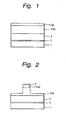
- FIGs. 1 through 3 show a method for making a sample for evaluation.
- an undoped GaN buffer layer 2 is grown by MOCVD under a temperature around 520 °C, for example, on a c-plane sapphire substrate 1 with a previously cleaned surface by thermal cleaning, for example. Thereafter, at the growth temperature of 1000 °C, an undoped GaN layer 3, p-type AlGaN buried layer 4 and p-type GaN layer 5 are sequentially grown on the GaN buffer layer 2 by MOCVD.
- Source materials for growing these GaN compound semiconductor layers may be, for example, trimethyl gallium ((CH 3 ) 3 Ga, TMG) as the source material of the group III element Ga, trimethyl aluminum ((CH 3 ) 3 Al, TMA) as the source material of the group III element Al, trimethyl indium ((CH 3 ) 3 In, TMI) as the source material of group III element In, and ammonium (NH 3 ) as the source material of the group V element N.
- the carrier gas may be a mixed gas of hydrogen (H 2 ) and nitrogen (N 2 ), for example.
- the c-plane sapphire substrate 1 having grown the GaN semiconductor layer is removed from the MOCVD apparatus. Then, as shown in Fig. 2, after making a SiO 2 film 6, 0.4 ⁇ m thick, on the entire surface of the p-type GaN layer 5 by CVD, vacuum evaporation, sputtering, or the like, a resist pattern (not shown) of a predetermined pattern is formed on the SiO 2 film 6 by lithography.
- the SiO 2 film 6 is etched to shape it into a stripe by wet etching using an etchant selected from a series of hydrofluoric acids, for example, or reactive ion etching (RIE) using an etching gas such as CF 4 or CHF 3 containing fluorine.
- RIE reactive ion etching
- the SiO 2 film 6 is etched to a certain depth thereof by RIE, for example, to form the ridge portion.
- the etching gas for RIE may be, for example, a chlorine-based gas.
- an AlGaN buried layer 7 containing Al by 60%, for example, is grown on the entire substrate surface to bury opposite sides of the ridge portion.
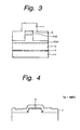
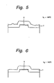
- Figs. 4 through 6 are diagrams drawn from scanning electronic microscopic photographs (SEM photographs) of cross sections of the ridge portion and adjacent AlGaN buried layer 7 in a sample prepared by setting the growth temperature (Tg) at 800 °C, 760 °C and 730 °C, respectively, for growth of the AlGaN buried layer 7.
- Tg growth temperature
- Figs. 4 through 6 when the growth temperature is 800 °C, the AlGaN buried layer 7 fails to bury portions along side surfaces of the ridge portion (hollow spaces).
- the surface of the AlGaN buried layer 7 is flat when the growth temperature is 730 °C, but becomes uneven as the growth temperature increases.
- the AlGaN buried layer 7 is single-crystalline when the growth temperature is 800 °C, but it is partly columnar-structured when the growth temperature is 760 °C. Additionally, when the growth temperature is 900 °C, although not shown, unevenness on the surface of the AlGaN buried layer 7 is not so large, but cracks are produced in the AlGaN buried layer 7. As reviewed above, the use of a single crystal layer to bury the ridge portion involves the problems, failure to bury side surfaces of the ridge portion, large unevenness on the surface and generation of cracks. Therefore, in order to reliably bury the ridge side surfaces and prevent cracks, the semiconductor layer used to bury the ridge portion must be polycrystalline at least partly.
- the growth temperature for growing the AlGaN buried layer 7 by MOCVD is preferably not higher than 760 °C.
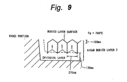
- Figs. 7 through 9 schematically show cross-sectional structures of AlGaN buried layers 7 observed through a transmission electronic microscope (TEM) in samples prepared by setting the growth temperature (Tg) at 520 °C, 730 °C and 760 °C, respectively, for growth of the AlGaN buried layer 7.
- Tg growth temperature
- the AlGaN buried layer 7 is epitaxially grown from the base layer as a single crystal at a part thereof in contact with the base layer, and the crystal grows thereon in form of columns to form a columnar structure. Thickness of the epitaxial layer was approximately 70 nm. Diameter of lower portions of columnar crystals were 50 through 80 nm. Unevenness as high as approximately 30 nm was produced on the surface of the AlGaN buried layer 7.
- the part of the AlGaN buried layer 7 in contact with the base layer exhibits a faultless single crystal epitaxially grown from the base layer, and above it, the crystal growc in a columnar form to make a columnar structure.
- Thickness of the epitaxial layer was approximately 130 nm, and diameter of a lower part of each columnar crystal was approximately 270 nm. These columnar crystals are substantially aligned in orientation. Further, a large number of planar defects were introduced into respective columnar crystals. There was unevenness as high as approximately 160 nm on the surface of the AlGaN buried layer 7.
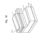
- Fig. 10 shows a GaN compound semiconductor laser having a buried ridge structure according to the first embodiment of the invention.
- the GaN compound semiconductor laser shown here has a SCH structure(separate confinement heterostructure).
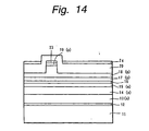
- the GaN semiconductor laser according to the first embodiment includes an n-type GaN contact layer 13, n-type AlGaN cladding layer 14, n-type GaN optical guide layer 15, active layer 16 having an undoped Ga 1-x In x N/Ga 1-y In y N multi quantum well structure, p-type GaN optical guide layer 17, p-type AlGaN cladding layer 18 and p-type GaN contact layer 19 sequentially stacked on a c-plane sapphire substrate 11 having the thickness of 400 ⁇ m, for example, via an undoped GaN buffer layer 12.
- the GaN buffer layer 12 is 30 nm thick, for example.
- the n-type GaN contact layer 13 is 4 ⁇ m thick, for example, and doped with silicon (Si), for example, as its n-type impurity.
- the n-type AlGaN cladding layer 14 is 0.7 ⁇ m thick, for example, and doped with Si, for example, as its n-type impurity.
- the n-type GaN optical guide layer 15 is 0.1 ⁇ m thick, for example, and doped with Si, for example, as its n-type impurity.
- each well layer is 3 nm thick and each barrier layer is 4 nm thick, for example.
- the p-type GaN optical guide layer 17 is 0.1 ⁇ m thick, and doped with magnesium (Mg), for example, as its p-type impurity.
- the p-type AlGaN cladding layer 18 is 0.7 ⁇ m thick, for example, and doped with Mg, for example, as its p-type impurity.
- the p-type GaN contact layer 19 is 0.3 ⁇ m thick, for example, and doped with Mg, for example, as its p-type impurity.
- the upper-lying portion of the n-type GaN contact layer 13, n-type AlGaN cladding layer 14, n-type GaN optical guide layer 15, active layer 16, p-type GaN optical guide layer 17 and p-type AlGaN cladding layer 18 have a mesa configuration of a predetermined width.
- the upper-lying portion of the p-type AlGaN cladding layer 18 and the p-type GaN contact layer 19 form a ridge portion with a predetermined width extending in one direction.
- the extending direction of the ridge portion may be ⁇ 11-20> direction, for example, and the width is 4 ⁇ m, for example.
- an undoped AlGaN buried layer 20 is provided at opposite sides of the ridge portion.
- the AlGaN buried layer 20 is polycrystalline (or columnar-structured) at least partly.
- a p-side electrode 21 is provided on the p-type GaN contact layer 19 and its adjacent portions of the AlGaN buried layer 20.
- the p-side electrode 21 has a Ni/Pt/Au structure sequentially stacking an Ni film, Pt film and Au film, for example, and these Ni film, Pt film and Au film are 10 nm thick, 100 nm thick and 300 nm thick, respectively, for example. Since the AlGaN buried layer 20 has a high resistance, current flows merely in the ridge stripe portion regardless of the p-side electrode 21 being in contact with both the GaN contact layer 19 and the AlGaN buried layer 20.
- an n-side electrode 22 is provided on the n-type GaN contact layer 13.
- the n-side electrode 22 has a Ti/Al/Pt/Au structure sequentially stacking a Ti film, Al film, Pt film and Au film, for example, and these Ti film, Al film, Pt film and Au film are 10 nm thick, 100 nm thick, 100 nm thick and 300 nm thick, respectively, for example.
- an undoped GaN buffer layer 12 is grown by MOCVD under a temperature around 520 °C, for example, on a c-plane sapphire substrate 11 with a previously cleaned surface by thermal cleaning, for example.
- the substrate temperature is increased to a predetermined growth temperature, and an n-type GaN layer 3, n-type AlGaN cladding layer 14, n-type GaN optical guide layer 15, active layer 16 having the undoped Ga 1-x In x N/Ga 1-y In y N multi quantum well structure, p-type GaN optical guide layer 17, p-type AlGaN cladding layer 18 and p-type GaN contact layer 19 are sequentially stacked on the GaN buffer layer 12.
- the growth temperature is set to 1000°C, for example.
- the active layer 16 having the Ga 1-x In x N/Ga 1-y In y N multi quantum well structure, which contains In the growth temperature is set to 700 through 800°C, for example.
- Source materials for growing these GaN compound semiconductor layers may be, for example, trimethyl gallium ((CH 3 ) 3 Ga, TMG) as the source material of the group III element Ga, trimethyl aluminum ((CH 3 ) 3 Al, TMA) as the source material of the group III element Al, trimethyl indium ((CH 3 ) 3 In, TMI) as the source material of group III element In, and ammonium (NH 3 ) as the source material of the group V element N.
- the carrier gas may be a mixed gas of hydrogen (H 2 ) and nitrogen (N 2 ), for example.
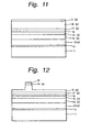
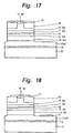
- the c-plane sapphire substrate 11 having grown the GaN semiconductor layer is removed from the MOCVD apparatus. Then, as shown in Fig. 12, after making a SiO 2 film 23, 0.4 ⁇ m thick, on the entire surface of the p-type GaN contact layer 19 by CVD, vacuum evaporation, sputtering, or the like, a resist pattern (not shown) of a predetermined pattern is formed on the SiO 2 film 23 by lithography.
- the SiO 2 film 23 is etched to shape it into a stripe by wet etching using an etchant selected from a series of hydrofluoric acids, for example, or RIE using an etching gas such as CF 4 or CHF 3 containing fluorine. Thereafter, using the SiO 2 film 23 as a mask, the p-type AlGaN cladding layer 18 is etched to a certain depth thereof by RIE, for example, to form the ridge portion.
- the etching gas for RIE may be, for example, a chlorine-based gas.
- an AlGaN buried layer 20 containing Al by 60% is grown on the entire substrate surface to bury opposite sides of the ridge portion.
- the growth temperature of 520°C at least a part of the AlGaN buried layer 20 becomes polycrystalline. In this case, no crack is produced in the AlGaN buried layer 20 even with the Al composition of 60%.
- the entirety of the ridge can be buried with good smoothness.
- the c-plane sapphire substrate 11 having the AlGaN buried layer 20 grown thereon is removed by the MOCVD apparatus.
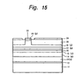
- a SiO 2 film 24, 0.4 ⁇ m thick, for example is formed on the entire substrate surface by CVD, vacuum evaporation or sputtering, for example, a resist pattern (not shown) of a predetermined configuration is made by lithography on the SiO 2 film 24 excluding the projecting portion of the AlGaN buried layer 20.
- the SiO 2 film 24 is etched by wet etching using an etchant selected from a series of hydrofluoric acids, for example, or RIE using an etching gas such as CF 4 or CHF 3 containing fluorine.
- an etchant selected from a series of hydrofluoric acids, for example, or RIE using an etching gas such as CF 4 or CHF 3 containing fluorine.
- etching is conducted by RIE, for example, to remove the projecting portion of the AlGaN buried layer 20 above the ridge portion.
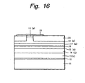
- the SiO 2 film 24 is removed, and a SiO 2 film 25 with a predetermined configuration is formed on the substrate surface in the same process as explained above as shown in Fig. 16.
- etching is conducted by RIE, for example, until exposing the n-type GaN contact layer 13, to pattern the upper-lying portion of the n-type GaN contact layer 13, n-type AlGaN cladding layer 14, n-type GaN optical guide layer 15, active layer 16 with the undoped Ga 1-x In x N/Ga 1-y In y N multi quantum well structure, p-type GaN optical guide layer 17, p-type AlGaN cladding layer 18 and AlGaN buried layer 20 into a mesa configuration.
- the SiO 2 film 25 is removed by etching.
- a resist pattern (not shown) of a predetermined configuration is formed on the substrate surface, and a Ti film, Al film, Pt film and Au film are formed sequentially on the entire substrate surface by vacuum evaporation, for example.
- the resist pattern is removed together with the overlying Ti film, Al film, Pt film and Au film (lift-off).
- the n-side electrode 22 is formed on a location of the n-type GaN contact layer 13 adjacent to the mesa portion. Thereafter, the n-side electrode 22 is alloyed for ohmic contact.
- the p-side electrode 21 is also formed in a similar process in the mesa portion on the p-type GaN contact layer 19 and its adjacent portions of the AlGaN buried layer 20, and it is alloyed for ohmic contact.
- the c-plane sapphire substrate 11 having formed the laser structure thereon is divided into bars by cleavage, for example, to form cavity edges.
- the cavity edges are next coated by edge coating, and each bar is divided into chips by cleavage, for example.
- the intended buried ridge structured and SCH structured GaN compound semiconductor laser is completed as shown in Fig. 10.
- Fig. 19 shows a result of measurement on optical output to current characteristics of the GaN compound semiconductor laser according to the first embodiment.
- the growth temperature of the AlGaN buries layer 20 is 520 °C. It is noted from Fig. 19 that good optical output to current characteristics were obtained.
- the ridge is buried by the AlGaN buried layer 20 grown at the growth temperature of 520 °C to be polycrystalline at least partly, the entirety of the ridge can be buried with good surface smoothness without producing cracks in the AlGaN buried layer 20 even with a high Al composition. Additionally, since the contact area between the p-side electrode 21 and the base layer can be increased, it is possible to effectively release heat generated during operation and prevent an increase of the current during supply of power to thereby elongate the lifetime of the semiconductor laser. Additionally, by changing the Al composition in the AlGaN buried layer 20, the difference in refractive index between the ridge portion and the remainder portion can be controlled, and transverse modes can be controlled easily.
- the first embodiment also has the following advantage. That is, in case of growth of GaN semiconductors, in general, there is the problem that a p-type impurity (acceptor) in grown layers is inactivated by hydrogen in the growth atmosphere, and there is the need for post-annealing in a nitrogen atmosphere after growth of p-type layers.
- the outer-most surface is the AlGaN buried layer 20 during growth of the AlGaN buried layer 20
- hydrogen in the growth atmosphere does not directly attack p-type layers, and hydrogen caught into p-type layers during first epitaxial growth for growing layers up to the p-type GaN contact layer 19 may leave therefrom through the AlGaN buried layer 20. Therefore, p-type impurities in p-type layers can be activated during growth of the AlGaN buried layer 20 without executing post-annealing.
- Fig. 20 shows a GaN compound semiconductor layer having a buried ridge structure according to the second embodiment of the invention.
- This GaN compound semiconductor laser also has a SCH structure.
- a high-resistance AlN buried layer 26 is buried at opposite sides of the ridge portion. At least a part of the AlN buried layer 26 is polycrystalline.
- the GaN compound semiconductor laser shown here is the same as that of the first embodiment. So, their explanation is omitted.
- the method for manufacturing the GaN compound semiconductor laser according to the second embodiment is the same as the manufacturing method of the GaN compound semiconductor laser according to the first embodiment except that the AlN buried layer 26 is made by ECR sputtering.
- the ridge is buried by the AlGaN buried layer 20 grown by ECR sputtering to be polycrystalline at least partly, the entirety of the ridge can be buried with good surface smoothness without producing cracks in the AlGaN buried layer 20. Additionally, since the contact area between the p-side electrode 21 and the base layer can be increased, it is possible to effectively release heat generated during operation and prevent an increase of the current during supply of power thereby to elongate the lifetime of the semiconductor laser.
- the refractive index of the AlN buried layer 26 is larger than that of SiO 2 or air, the difference in refractive index between the ridge portion and the remainder portion can be reduced as compared with conventional ridge-structured GaN compound semiconductor lasers, and transverse modes can be stabilized. Furthermore, since the AlN buried layer 26 is made by ECR sputtering, the burying process is easier.
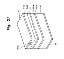
- Fig. 21 shows a GaAs compound semiconductor laser having a buried ridge structure according to the third embodiment of the invention.
- the GaAs compound semiconductor laser according to the third embodiment includes an n-type GaAs buffer layer 32, n-type AlGaAs cladding layer 33, active layer 34 with a single quantum well structure or a multi quantum well structure, p-type AlGaAs cladding layer 35 and p-type GaAs cap layer 36 which are sequentially stacked on an n-type GaAs substrate 31.
- An upper-lying portion of the p-type AlGaAs cladding layer 35 and the p-type GaAs cap layer 36 form a ridge portion of a predetermined width extending in one direction.
- an n-type AlGaAs buried layer 37 is buried. At least a part of the n-type AlGaAs buried layer 37 is made up of a polycrystalline or amorphous region.
- a p-side electrode 38 is provided on the p-type GaAs cap layer 36 and its adjacent portions of the n-type AlGaAs buried layer 37.
- the p-side electrode 38 may be, for example, a Ti/Pt/Au electrode.
- an n-side electrode 39 is provided in ohmic contact with the n-type GaAs substrate 31.
- the n-side electrode 39 may be, for example, a AuGe/Ni electrode or an In electrode.
- the n-type GaAs buffer layer 32, n-type AlGaAs cladding layer 33, active layer 34, p-type AlGaAs cladding layer 35 and p-type GaAs cap layer 36 are sequentially grown on the n-type GaAs substrate 31 by metal organic chemical vapor deposition (MOCVD), for example, at a growth temperature around 800 °C, for example.
- MOCVD metal organic chemical vapor deposition
- the n-type GaAs substrate 31 having the AlGaAs compound semiconductor layers grown thereon is removed from the MOCVD apparatus.
- the SiO 2 film is etched to shape it into a stripe by wet etching using an etchant selected from a series of hydrofluoric acids, for example, or RIE using an etching gas such as CF 4 or CHF 3 containing fluorine. Then, using the SiO 2 film as a mask, the p-type AlGaAs cladding layer 35 is etched to a predetermined depth by wet etching or dry etching to form a ridge portion.
- an etchant selected from a series of hydrofluoric acids, for example, or RIE using an etching gas such as CF 4 or CHF 3 containing fluorine.
- the n-type AlGaAs buried layer is grown on the entire surface again by MOCVD at the growth temperature of 450 °C, for example, to bury opposite sides of the ridge portion.
- the n-type AlGaAs buried layer 37 becomes polycrystalline or amorphous at least partly. In this case, no cross hatching is produced in the n-type AlGaAs buried layer 37, and the entire ridge can be buried with good surface smoothness.
- the n-type GaAs substrate 31 having the n-type AlGaAs buried layer 37 thereon is removed from the MOCVD apparatus.
- the SiO 2 film is etched to shape it into a stripe by wet etching using an etchant selected from a series of hydrofluoric acids, for example, or RIE using an etching gas such as CF 4 or CHF 3 containing fluorine.
- an etchant selected from a series of hydrofluoric acids, for example, or RIE using an etching gas such as CF 4 or CHF 3 containing fluorine.
- etching by wet etching or RIE is conducted to remove the projecting portion of the n-type AlGaAs buried layer 37 above the ridge portion. Thereafter, the SiO 2 film is removed by etching.
- a Ti film, Pt film and Au film are sequentially stacked on the entire surface of the substrate by vacuum evaporation, for example, to form the p-side electrode 38.
- a AuGe/Ni film or an In film is formed as the n-side electrode 39.
- the n-type GaAs substrate 31 having formed the laser structure thereon is devided into bars by cleavage, for example, to form cavity edges.
- the cavity edges are next coated by edge coating, and each bar is devided into chips by cleavage, for example.
- the same advantages as those of the first embodiment can be obtained in ridge-structured GaAs semiconductor lasers.
- numerical values, structures, substrates, source materials and processes proposed in the first, second and third embodiments are not but examples, and other appropriate numerical values, structures, substrates, source materials and processes may be used, if necessary.
- first and second embodiments have been explained as extending the ridge stripe portion in the ⁇ 11-20> orientation of the c-plane sapphire substrate 11, it may instead extend in the ⁇ 1-100> direction.
- first and second embodiments have been explained as using the c-plane sapphire substrate as the substrate, a SiC substrate, Si substrate of spinel substrate, for example, may be used where appropriate.
- first and second embodiments have been explained as applying the invention to SCH-structured GaN compound semiconductor lasers.
- the invention is also applicable to GaN compound semiconductor lasers having a DH structure (double heterostructure), for example.
- the third embodiment has been explained as applying the invention to GaAs compound semiconductor lasers having a DH structure (double heterostructure). However, it is applicable to SCH-structured GaAs compound semiconductor lasers as well.
- the semiconductor laser since opposite sides of the ridge are buried by the buried semiconductor layer made of a compound semiconductor or a nitride III-V compound semiconductor at least a part of which is a non-single crystal, high-order mode oscillation can be prevented by stably controlling transverse modes, and excellent heat dissipation is ensured.
- the semiconductor laser having the said advantages can be manufactured easily.
- the semiconductor device since opposite sides of the projection are buried by the buried semiconductor layer made of a compound semiconductor or a nitride III-V compound semiconductor at least a part of which is a non-single crystal, and excellent heat dissipation is ensured.
- the semiconductor device having the said advantages can be manufactured easily.
Landscapes
- Physics & Mathematics (AREA)
- Condensed Matter Physics & Semiconductors (AREA)
- General Physics & Mathematics (AREA)
- Electromagnetism (AREA)
- Optics & Photonics (AREA)
- Geometry (AREA)
- Semiconductor Lasers (AREA)
Description
Claims (42)
- A semiconductor laser using a compound semiconductor and having a ridge-shaped stripe, comprising:characterized in thata buried semiconductor layer made of a compound semiconductor at least a part of which is a non-single crystal, and burying opposite sides of the ridge
said buried semiconductor layer is at least partly polycrystalline. - A semiconductor laser according to claim 1, wherein said semiconductor laser uses a nitride III-V compound semiconductor.
- The semiconductor laser according to claim 1 or 2, wherein said buried semiconductor layer is made of a nitride III-V compound semiconductor.
- The semiconductor laser according to claim 3, wherein said buried semiconductor layer includes a region of a single crystal and a region of a polycrystal.
- The semiconductor laser according to claim 3. wherein said buried semiconductor layer has a columnar structure.
- The semiconductor laser according to claim 5 wherein diameter of a columnar crystal forming said buried semiconductor layer is in the range from 5 nm to 300 nm.
- The semiconductor laser according to claim 3. wherein said buried semiconductor layer has a refractive index not higher than that of an active layer.
- The semiconductor laser according to claim 3. wherein said buried semiconductor layer is made of AlxGa1-xN (0≤x≤1).
- The semiconductor laser according to claim 3. wherein said semiconductor laser is a real index-guided semiconductor laser.
- A manufacturing method of a semiconductor laser using a compound semiconductor and having a ridge-shaped stripe, comprising the steps of:forming said ridge-shaped stripe;growing a buried semiconductor layer of a compound semiconductor to cover the ridge at a growth temperature such that at least a part of said buried semiconductor layer at opposite sides of the ridge be a polycrystal; andremoving a part of said buried semiconductor layer from above said ridge.
- A manufacturing method of a semiconductor laser according to claim 10, wherein said semiconductor laser uses a nitride III-V compound semiconductor.
- The manufacturing method of a semiconductor laser according to claim 11, wherein said buried semiconductor layer is made of a nitride III-V compound semiconductor.
- The manufacturing method of a semiconductor laser according to claim 12, wherein said buried semiconductor layer includes a region of a single crystal and a region of a polycrystal.
- The manufacturing method of a semiconductor laser according to claim 12, wherein said buried semiconductor layer has a columnar structure.
- The manufacturing method of a semiconductor laser according to claim 14, wherein diameter of a columnar crystal forming said buried semiconductor layer is in the range from 5 nm to 300 nm.
- The manufacturing method of a semiconductor laser according to claim 12, wherein said buried semiconductor layer is grown under a growth temperature not lower than the decomposition temperature of a source material for growth thereof and not higher than 760 °C.
- The manufacturing method of a semiconductor laser according to claim 12, wherein said buried semiconductor layer is grown under a growth temperature in the range from 480 °C to 760 °C.
- The manufacturing method of a semiconductor laser according to claim 12, wherein said buried semiconductor layer is grown under a growth temperature in the range from 520 °C to 760 °C.
- The manufacturing method of a semiconductor laser according to claim 12, wherein said buried semiconductor layer is grown by metal organic chemical vapor deposition, hydride vapor phase epitaxial growth or molecular beam epitaxy.
- The manufacturing method of a semiconductor laser according to claim 12, wherein said buried semiconductor layer is grown by electron cyclotron resonance sputtering.
- The manufacturing method of a semiconductor laser according to claim 12, wherein said buried semiconductor layer has a refractive index not higher than that of an active layer.
- The manufacturing method of a semiconductor laser according to claim 12, wherein said buried semiconductor layer is made of AlxGa1-xN (0≤x≤1).
- The manufacturing method of a semiconductor laser according to claim 12, wherein said semiconductor laser is a real index-guided semiconductor laser.
- A semiconductor device comprising:characterized in thata compound semiconductor base body having a projection: and
a buried semiconductor layer made of a compound semiconductor at least a part of which is a non-single crystal, and provided to bury said projection
said buried semiconductor layer is at least partly polycrystalline. - A semiconductor device according to claim 24, wherein
said base body is made of a nitride III-V compound semiconductor. - The semiconductor device according to claim 25, wherein said buried semiconductor layer is made of a nitride III-V compound semiconductor.
- The semiconductor device according to claim 26, wherein said buried semiconductor layer includes a region of a single crystal and a region of a polycrystal.
- The semiconductor device according to claim 26, wherein said buried semiconductor layer has a columnar structure.
- The semiconductor device according to claim 28, wherein diameter of a columnar crystal forming said buried semiconductor layer is in the range from 5 nm to 300 nm.
- The semiconductor device according to claim 26, wherein said buried semiconductor layer is made of AIxGa1-xN (0≤x≤1).
- A manufacturing method of a semiconductor device having a base body made of a compound semiconductor and having a projection, and having a buried semiconductor layer made of a compound semiconductor at least a part of which is a non-single crystal so as to bury said projection, comprising the steps of:forming said projection;growing a buried semiconductor layer of a compound semiconductor to cover said projection at a growth temperature such that at least a part of said buried semiconductor layer around said projection be a polycrystal; andremoving a part of said buried semiconductor layer from above said projection.
- A manufacturing method of a semiconductor device according to claim 31, wherein said base body is made of a nitride III-V compound semiconductor.
- The manufacturing method of a semiconductor device according to claim 32, wherein said buried semiconductor layer is made of a nitride III-V compound semiconductor.
- The manufacturing method of a semiconductor device according to claim 33, wherein said buried semiconductor layer includes a region of a single crystal and a region of a polycrystal.
- The manufacturing method of a semiconductor device according to claim 33, wherein said buried semiconductor layer has a columnar structure.
- The manufacturing method of a semiconductor device according to claim 35 wherein diameter of a columnar crystal forming said buried semiconductor layer is in the range from 5 nm to 300 nm.
- The manufacturing method of a semiconductor device according to claim 33, wherein said buried semiconductor layer is grown under a growth temperature not lower than the decomposition temperature of a source material for growth thereof and not higher than 760 °C.
- The manufacturing method of a semiconductor device according to claim 33, wherein said buried semiconductor layer is grown under a growth temperature in the range from 480 °C to 760 °C.
- The manufacturing method of a semiconductor device according to claim 33, wherein said buried semiconductor layer is grown under a growth temperature in the range from 520 °C to 760 °C.
- The manufacturing method of a semiconductor device according to claim 33, wherein said buried semiconductor layer is grown by metal organic chemical vapor deposition, hydride vapor phase epitaxial growth or molecular beam epitaxy.
- The manufacturing method of a semiconductor device according to claim 33, wherein said buried semiconductor layer is grown by electron cyclotron resonance sputtering.
- The manufacturing method of a semiconductor device according to claim 33, wherein said buried semiconductor layer is made of AlxGa1-xN (0≤x≤1).
Applications Claiming Priority (4)
| Application Number | Priority Date | Filing Date | Title |
|---|---|---|---|
| JP33635498 | 1998-11-26 | ||
| JP33635498 | 1998-11-26 | ||
| JP11680599 | 1999-04-23 | ||
| JP11680599A JP3804335B2 (en) | 1998-11-26 | 1999-04-23 | Semiconductor laser |
Publications (3)
| Publication Number | Publication Date |
|---|---|
| EP1005123A2 EP1005123A2 (en) | 2000-05-31 |
| EP1005123A3 EP1005123A3 (en) | 2003-04-02 |
| EP1005123B1 true EP1005123B1 (en) | 2005-03-02 |
Family
ID=26455051
Family Applications (1)
| Application Number | Title | Priority Date | Filing Date |
|---|---|---|---|
| EP99123020A Expired - Lifetime EP1005123B1 (en) | 1998-11-26 | 1999-11-19 | Semiconductor laser, semiconductor device and their manufacturing methods |
Country Status (5)
| Country | Link |
|---|---|
| EP (1) | EP1005123B1 (en) |
| JP (1) | JP3804335B2 (en) |
| KR (1) | KR100639747B1 (en) |
| DE (1) | DE69923919T2 (en) |
| TW (1) | TW443016B (en) |
Cited By (1)
| Publication number | Priority date | Publication date | Assignee | Title |
|---|---|---|---|---|
| US8649408B2 (en) | 2010-03-04 | 2014-02-11 | Kabushiki Kaisha Toshiba | Semiconductor laser device |
Families Citing this family (8)
| Publication number | Priority date | Publication date | Assignee | Title |
|---|---|---|---|---|
| TW451504B (en) * | 2000-07-28 | 2001-08-21 | Opto Tech Corp | Compound semiconductor device and method for making the same |
| JP4826019B2 (en) * | 2001-02-16 | 2011-11-30 | ソニー株式会社 | Manufacturing method of semiconductor laser device |
| JP2002335048A (en) | 2001-03-06 | 2002-11-22 | Sony Corp | Nitride semiconductor laser element and its manufacturing method |
| JP5013463B2 (en) * | 2007-05-22 | 2012-08-29 | シャープ株式会社 | Nitride semiconductor laser device and manufacturing method thereof |
| DE102007057756B4 (en) * | 2007-11-30 | 2022-03-10 | OSRAM Opto Semiconductors Gesellschaft mit beschränkter Haftung | Process for producing an optoelectronic semiconductor body |
| JP2011096870A (en) * | 2009-10-30 | 2011-05-12 | Nichia Corp | Nitride semiconductor laser element |
| KR20130079873A (en) * | 2012-01-03 | 2013-07-11 | 엘지이노텍 주식회사 | Light emitting device and lighting system including the same |
| DE102014105191B4 (en) * | 2014-04-11 | 2019-09-19 | Osram Opto Semiconductors Gmbh | Semiconductor strip laser and semiconductor device |
Family Cites Families (4)
| Publication number | Priority date | Publication date | Assignee | Title |
|---|---|---|---|---|
| JPS61168981A (en) * | 1985-01-23 | 1986-07-30 | Hitachi Ltd | Semiconductor laser device |
| US5777350A (en) * | 1994-12-02 | 1998-07-07 | Nichia Chemical Industries, Ltd. | Nitride semiconductor light-emitting device |
| JP3905935B2 (en) * | 1995-09-01 | 2007-04-18 | 株式会社東芝 | Semiconductor device and method for manufacturing semiconductor device |
| JP3448450B2 (en) * | 1996-04-26 | 2003-09-22 | 三洋電機株式会社 | Light emitting device and method for manufacturing the same |
-
1999
- 1999-04-23 JP JP11680599A patent/JP3804335B2/en not_active Expired - Fee Related
- 1999-11-17 TW TW088120089A patent/TW443016B/en not_active IP Right Cessation
- 1999-11-19 EP EP99123020A patent/EP1005123B1/en not_active Expired - Lifetime
- 1999-11-19 DE DE69923919T patent/DE69923919T2/en not_active Expired - Lifetime
- 1999-11-25 KR KR1019990052589A patent/KR100639747B1/en not_active IP Right Cessation
Cited By (1)
| Publication number | Priority date | Publication date | Assignee | Title |
|---|---|---|---|---|
| US8649408B2 (en) | 2010-03-04 | 2014-02-11 | Kabushiki Kaisha Toshiba | Semiconductor laser device |
Also Published As
| Publication number | Publication date |
|---|---|
| KR100639747B1 (en) | 2006-10-31 |
| DE69923919T2 (en) | 2006-04-06 |
| EP1005123A2 (en) | 2000-05-31 |
| JP2000223781A (en) | 2000-08-11 |
| KR20000035669A (en) | 2000-06-26 |
| EP1005123A3 (en) | 2003-04-02 |
| DE69923919D1 (en) | 2005-04-07 |
| TW443016B (en) | 2001-06-23 |
| JP3804335B2 (en) | 2006-08-02 |
Similar Documents
| Publication | Publication Date | Title |
|---|---|---|
| US6232623B1 (en) | Semiconductor device on a sapphire substrate | |
| US8587004B2 (en) | Semiconductor light emitting device, its manufacturing method, semiconductor device and its manufacturing method | |
| JP3785970B2 (en) | Method for manufacturing group III nitride semiconductor device | |
| US20100317136A1 (en) | Method for producing semiconductor light emitting device, method for producing semiconductor device, method for producing device, method for growing nitride type iii-v group compound semiconductor layer, method for growing semiconductor layer, and method for growing layer | |
| US20020027933A1 (en) | Semiconductor light emitting device and semiconductor laser | |
| US7755101B2 (en) | Semiconductor light emitting device | |
| KR20020071787A (en) | Group ⅲ-ⅴ compound semiconductor crystal structure and method of epitaxial growth of the same as well as semiconductor device including the same | |
| JP2001094212A (en) | Semiconductor element and its manufacturing method | |
| US6620641B2 (en) | Semiconductor light emitting device and its manufacturing method | |
| EP1005123B1 (en) | Semiconductor laser, semiconductor device and their manufacturing methods | |
| US6577662B1 (en) | Semiconductor laser, and manufacturing method thereof, semiconductor device and manufacturing method thereof | |
| JP4625998B2 (en) | Nitride semiconductor laser device | |
| JP2000183451A (en) | Semiconductor laser element and its manufacturing method | |
| JP3900196B2 (en) | Group III nitride semiconductor optical device | |
| JPH10261614A (en) | Selective etching method of nitride base compound semiconductor, and semiconductor device | |
| JP4415440B2 (en) | Manufacturing method of semiconductor laser | |
| JP3975971B2 (en) | Manufacturing method of semiconductor laser | |
| JP4049200B2 (en) | Group III nitride semiconductor optical device | |
| JP2006013476A (en) | Iii-v compound semiconductor and its manufacturing method, and semiconductor device | |
| JP2000164985A (en) | Semiconductor laser | |
| JP2001274517A (en) | Substrate for semiconductor element, method for manufacturing the same and semiconductor element using the substrate for semiconductor element |
Legal Events
| Date | Code | Title | Description |
|---|---|---|---|
| PUAI | Public reference made under article 153(3) epc to a published international application that has entered the european phase |
Free format text: ORIGINAL CODE: 0009012 |
|
| AK | Designated contracting states |
Kind code of ref document: A2 Designated state(s): AT BE CH CY DE DK ES FI FR GB GR IE IT LI LU MC NL PT SE |
|
| AX | Request for extension of the european patent |
Free format text: AL;LT;LV;MK;RO;SI |
|
| PUAL | Search report despatched |
Free format text: ORIGINAL CODE: 0009013 |
|
| AK | Designated contracting states |
Kind code of ref document: A3 Designated state(s): AT BE CH CY DE DK ES FI FR GB GR IE IT LI LU MC NL PT SE Designated state(s): AT BE CH CY DE DK ES FI FR GB GR IE IT LI LU MC NL PT SE |
|
| AX | Request for extension of the european patent |
Extension state: AL LT LV MK RO SI |
|
| 17P | Request for examination filed |
Effective date: 20030902 |
|
| 17Q | First examination report despatched |
Effective date: 20031009 |
|
| AKX | Designation fees paid |
Designated state(s): DE FR GB |
|
| GRAP | Despatch of communication of intention to grant a patent |
Free format text: ORIGINAL CODE: EPIDOSNIGR1 |
|
| GRAS | Grant fee paid |
Free format text: ORIGINAL CODE: EPIDOSNIGR3 |
|
| GRAA | (expected) grant |
Free format text: ORIGINAL CODE: 0009210 |
|
| AK | Designated contracting states |
Kind code of ref document: B1 Designated state(s): DE FR GB |
|
| REG | Reference to a national code |
Ref country code: GB Ref legal event code: FG4D |
|
| REG | Reference to a national code |
Ref country code: IE Ref legal event code: FG4D |
|
| REF | Corresponds to: |
Ref document number: 69923919 Country of ref document: DE Date of ref document: 20050407 Kind code of ref document: P |
|
| PLBE | No opposition filed within time limit |
Free format text: ORIGINAL CODE: 0009261 |
|
| STAA | Information on the status of an ep patent application or granted ep patent |
Free format text: STATUS: NO OPPOSITION FILED WITHIN TIME LIMIT |
|
| 26N | No opposition filed |
Effective date: 20051205 |
|
| ET | Fr: translation filed | ||
| REG | Reference to a national code |
Ref country code: GB Ref legal event code: 746 Effective date: 20091130 |
|
| PGFP | Annual fee paid to national office [announced via postgrant information from national office to epo] |
Ref country code: FR Payment date: 20121130 Year of fee payment: 14 |
|
| PGFP | Annual fee paid to national office [announced via postgrant information from national office to epo] |
Ref country code: GB Payment date: 20121120 Year of fee payment: 14 |
|
| GBPC | Gb: european patent ceased through non-payment of renewal fee |
Effective date: 20131119 |
|
| REG | Reference to a national code |
Ref country code: FR Ref legal event code: ST Effective date: 20140731 |
|
| PG25 | Lapsed in a contracting state [announced via postgrant information from national office to epo] |
Ref country code: GB Free format text: LAPSE BECAUSE OF NON-PAYMENT OF DUE FEES Effective date: 20131119 Ref country code: FR Free format text: LAPSE BECAUSE OF NON-PAYMENT OF DUE FEES Effective date: 20131202 |
|
| PGFP | Annual fee paid to national office [announced via postgrant information from national office to epo] |
Ref country code: DE Payment date: 20141119 Year of fee payment: 16 |
|
| REG | Reference to a national code |
Ref country code: DE Ref legal event code: R119 Ref document number: 69923919 Country of ref document: DE |
|
| PG25 | Lapsed in a contracting state [announced via postgrant information from national office to epo] |
Ref country code: DE Free format text: LAPSE BECAUSE OF NON-PAYMENT OF DUE FEES Effective date: 20160601 |