EP1440332B1 - Röntgenbilderfassungsvorrichtung - Google Patents
Röntgenbilderfassungsvorrichtung Download PDFInfo
- Publication number
- EP1440332B1 EP1440332B1 EP02802814.0A EP02802814A EP1440332B1 EP 1440332 B1 EP1440332 B1 EP 1440332B1 EP 02802814 A EP02802814 A EP 02802814A EP 1440332 B1 EP1440332 B1 EP 1440332B1
- Authority
- EP
- European Patent Office
- Prior art keywords
- ray
- image acquisition
- acquisition apparatus
- ray image
- cells
- Prior art date
- Legal status (The legal status is an assumption and is not a legal conclusion. Google has not performed a legal analysis and makes no representation as to the accuracy of the status listed.)
- Expired - Lifetime
Links
- 238000006243 chemical reaction Methods 0.000 claims description 103
- 230000005855 radiation Effects 0.000 claims description 48
- 230000003287 optical effect Effects 0.000 claims description 32
- 239000000463 material Substances 0.000 claims description 11
- 230000004044 response Effects 0.000 claims description 11
- 230000026954 response to X-ray Effects 0.000 claims description 6
- DNYQQHLXYPAEMP-UHFFFAOYSA-N [I].[Cs] Chemical compound [I].[Cs] DNYQQHLXYPAEMP-UHFFFAOYSA-N 0.000 claims description 3
- 238000010521 absorption reaction Methods 0.000 claims description 3
- 229910021417 amorphous silicon Inorganic materials 0.000 claims description 3
- 229910052797 bismuth Inorganic materials 0.000 claims description 3
- JCXGWMGPZLAOME-UHFFFAOYSA-N bismuth atom Chemical compound [Bi] JCXGWMGPZLAOME-UHFFFAOYSA-N 0.000 claims description 3
- 229910052793 cadmium Inorganic materials 0.000 claims description 3
- BDOSMKKIYDKNTQ-UHFFFAOYSA-N cadmium atom Chemical compound [Cd] BDOSMKKIYDKNTQ-UHFFFAOYSA-N 0.000 claims description 3
- PBYZMCDFOULPGH-UHFFFAOYSA-N tungstate Chemical compound [O-][W]([O-])(=O)=O PBYZMCDFOULPGH-UHFFFAOYSA-N 0.000 claims description 3
- 238000001228 spectrum Methods 0.000 claims description 2
- 238000003384 imaging method Methods 0.000 description 19
- 238000000034 method Methods 0.000 description 7
- 230000008569 process Effects 0.000 description 6
- 230000008901 benefit Effects 0.000 description 5
- RYGMFSIKBFXOCR-UHFFFAOYSA-N Copper Chemical compound [Cu] RYGMFSIKBFXOCR-UHFFFAOYSA-N 0.000 description 3
- MCVAAHQLXUXWLC-UHFFFAOYSA-N [O-2].[O-2].[S-2].[Gd+3].[Gd+3] Chemical compound [O-2].[O-2].[S-2].[Gd+3].[Gd+3] MCVAAHQLXUXWLC-UHFFFAOYSA-N 0.000 description 3
- 229910052802 copper Inorganic materials 0.000 description 3
- 239000010949 copper Substances 0.000 description 3
- 230000001902 propagating effect Effects 0.000 description 3
- 239000000758 substrate Substances 0.000 description 3
- OAICVXFJPJFONN-UHFFFAOYSA-N Phosphorus Chemical compound [P] OAICVXFJPJFONN-UHFFFAOYSA-N 0.000 description 2
- 230000009471 action Effects 0.000 description 2
- 239000000853 adhesive Substances 0.000 description 2
- 230000001070 adhesive effect Effects 0.000 description 2
- 238000007689 inspection Methods 0.000 description 2
- 210000004872 soft tissue Anatomy 0.000 description 2
- 210000000988 bone and bone Anatomy 0.000 description 1
- 238000002405 diagnostic procedure Methods 0.000 description 1
- 238000010586 diagram Methods 0.000 description 1
- 230000000694 effects Effects 0.000 description 1
- 238000005286 illumination Methods 0.000 description 1
- CPLXHLVBOLITMK-UHFFFAOYSA-N magnesium oxide Inorganic materials [Mg]=O CPLXHLVBOLITMK-UHFFFAOYSA-N 0.000 description 1
- 239000000395 magnesium oxide Substances 0.000 description 1
- AXZKOIWUVFPNLO-UHFFFAOYSA-N magnesium;oxygen(2-) Chemical compound [O-2].[Mg+2] AXZKOIWUVFPNLO-UHFFFAOYSA-N 0.000 description 1
- 239000000203 mixture Substances 0.000 description 1
- 238000012986 modification Methods 0.000 description 1
- 230000004048 modification Effects 0.000 description 1
- 239000000843 powder Substances 0.000 description 1
- 210000001519 tissue Anatomy 0.000 description 1
Images

Classifications
-
- G—PHYSICS
- G01—MEASURING; TESTING
- G01T—MEASUREMENT OF NUCLEAR OR X-RADIATION
- G01T1/00—Measuring X-radiation, gamma radiation, corpuscular radiation, or cosmic radiation
- G01T1/16—Measuring radiation intensity
- G01T1/20—Measuring radiation intensity with scintillation detectors
- G01T1/2002—Optical details, e.g. reflecting or diffusing layers
-
- G—PHYSICS
- G01—MEASURING; TESTING
- G01T—MEASUREMENT OF NUCLEAR OR X-RADIATION
- G01T1/00—Measuring X-radiation, gamma radiation, corpuscular radiation, or cosmic radiation
- G01T1/16—Measuring radiation intensity
- G01T1/20—Measuring radiation intensity with scintillation detectors
- G01T1/2018—Scintillation-photodiode combinations
- G01T1/20187—Position of the scintillator with respect to the photodiode, e.g. photodiode surrounding the crystal, the crystal surrounding the photodiode, shape or size of the scintillator
Definitions
- the present invention relates, in general, to image acquisition and specifically to X-ray image acquisition.
- a typical X-ray image acquisition apparatus suitable for low energy X-rays includes a phosphor X-ray conversion screen and a photo detector array aligned with each other.
- the phosphor conversion screen generates optical light photons in response to the X-ray radiation.
- the optical light photons are transmitted to the photo detector array under the conversion screen.
- the photo detector array generates electric signals in response to the optical light photons.
- Electronics circuitry coupled to the photo detector array processes the electric signals and generate images.
- a typical high energy X-ray image acquisition apparatus includes a copper screen and a Gadolinium Oxysulfide panel over a photo detector array.
- the high energy X-ray radiation passes through the copper screen, which absorbs a portion of the X-ray radiation and generates energetic electrons.
- the electrons pass into the Gadolinium Oxysulfide panel and generate optical light photons.
- Another portion of the X-ray radiation passes through the copper screen and interacts with Gadolinium Oxysulfide to produce optical light photons.
- the photo detector array senses the optical light photons and generates electric signals in response thereto.
- X-ray images are generally used in soft tissue diagnostics, and high energy X-rays are used for treatment in radiation oncology and imaging are produced with imaging systems in conjunction with the treatment.
- the quality of the acquired image depends on the image acquisition procedures and the equipment used.
- X-ray images at different energy levels are presently created using different image acquisition apparatuses as described above. Maintaining multiple sets of X-ray image apparatuses will increase the operating and overhead costs for a medical diagnostic facility. It will also affect the efficiency of the facility by increasing the idle time of the apparatuses. These effects are exacerbated further for those facilities with relatively small patient bases.
- an apparatus that is capable of forming X-ray images with X-rays at different energy levels. It is desirable for the apparatus to be simple and reliable. It is also desirable if the apparatus can be used on an existing X-ray imaging system. It would be of further advantage to be able to optimize the image quality for its intended use.
- U.S. Patent No. 6,114,703 discloses a radiation imaging device having a two-dimensional array of scintillator elements, the array having a height of 1, 2 or 3 cm, wherein a photo detector array is arranged below the scintillator array such that each scintillator element is aligned with a photo detector.
- the present invention provides an X-ray image acquisition apparatus as defined in claim 1.
- a primary benefit of the present invention is providing an apparatus capable of forming X-ray images with X-rays at different energy levels.
- a particular benefit of some embodiments of the present invention is providing the apparatus that is simple and reliable.
- a specific benefit of some embodiments of the present invention is providing the apparatus that can be used on existing X-ray imaging systems.
- An additional benefit in accordance with some embodiments of the present invention is providing the apparatus that is capable of optimizing the image quality for its intended use.
- an X-ray image acquisition apparatus includes an X-ray conversion panel aligned with a photo detector array.
- the X-ray conversion panel generates optical light photons in response to the X-ray radiation of different energy levels.
- the photo detector array generates electric signals in response to the optical light photon received from the X-ray conversion panel.
- the conversion panel is made up of a plurality of X-ray conversion cells arranged in a two-dimensional array. Each conversion cell has a conversion body in its core.
- the conversion body is made of a scintillating material, e.g., Cesium Iodine, Bismuth Germanate, Cadmium Tungstate, etc., that generates optical light photons in response to X-ray radiation illuminating thereon and is substantially transparent to the generated optical light photons.
- the conversion bodies are sufficiently long to absorb the X-ray radiation over a wide range of energy levels.
- Light reflective films are attached to the sidewalls of the conversion bodies to collimate the optical light photons generated in the conversion bodies.
- the cross-section areas of the conversion bodies are sufficiently small to provide a satisfactory spatial resolution of the X-ray image generated using the conversion panel.
- the top of each conversion body is covered with an X-ray transparent and light reflective film. This film reflects those optical light photons generated in the conversion bodies and propagating away from the photo detector array, thereby increasing the efficiency of the conversion panel.
- the photo detector array includes an array of photo detectors aligned with the conversion cells in the conversion panel and generating electric signals in response to the optical light photons received from the corresponding conversion cells in the conversion panel.
- Electronics circuits coupled to the photo detector array process the electric signals and generate the images.
- FIG. 1 is a block diagram schematically illustrating an X-ray imaging system 10 in accordance with an embodiment of the present invention.
- X-ray imaging system 10 includes an X-ray radiation source 11 generating X-ray radiation 12 and an X-ray image acquisition apparatus 15.
- radiation source 11 is capable of generating X-ray radiation 12 at various energy levels.
- radiation source 11 is able to generate X-ray radiation 12 at a plurality of photon energy levels ranging between approximately 40 kilo-electron-volts (keV) to approximately 20 mega-electron-volts (MeV).
- keV kilo-electron-volts
- MeV mega-electron-volts
- X-ray radiation 12 is used to form images an object 14 placed between radiation source 11 and X-ray image acquisition apparatus 15.
- object 14 depends on the application of X-ray imaging system 10.
- X-ray imaging system 10 is a piece of medical diagnostic equipment and object 14 is a patient.
- X-ray imaging system 10 is a structure inspection equipment and object 14 is a machine part to be inspected.
- X-ray imaging system 10 is a security or custom inspection equipment and object 14 is a piece of luggage or cargo to be inspected. It should be understood that these examples are not meant to be exhaustive regarding the applications of X-ray imaging system 10.
- X-ray image acquisition apparatus 15 includes an X-ray conversion panel 20 and a photo detector array 40 suitable aligned with each other. During an imaging process, X-ray radiation 12 illuminates X-ray image acquisition apparatus 15. As shown in Fig. 1 , portions of X-ray radiation 12 reaches X-ray image acquisition apparatus 15 after passing through object 14. Because of their compositions and densities, different parts of object 14, e.g., different tissues in the body of a patient, may attenuate X-ray radiation 12 differently. For example, the bones in a patient generally attenuate X-ray radiation 12 more significantly than the soft tissues. In response to X-ray radiation 12 illuminating thereon, X-ray image acquisition apparatus 15 generates electric signals. Electronic circuits 16 coupled to x-ray image acquisition apparatus 15 processes the electric signals and generates the X-ray images of object 14 at a display device 18.
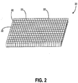
- Figure 2 schematically shows X-ray conversion panel 20 in X-ray image acquisition apparatus 15 in accordance with an embodiment of the present invention.
- Panel 20 includes a plurality of cells 22.
- cells 22 are arranged in a two-dimensional array a plurality of rows and a plurality of columns.
- Cells 22, which are also referred to as X-ray conversion cells or conversion cells are configured to generate optical light photons in response to X-ray radiation 12 shown in Fig. 1 .
- adhesive is used to form conversion panel 20 from X-ray conversion cells 22.
- a grid (not shown) is used to arrange conversion cells 22 into the two-dimensional array of X-ray conversion panel 20.
- Other means can also be used to form the array of X-ray conversion panel 20 using conversion cells 22.
- FIG. 3 is a schematic cross sectional view of an X-ray conversion cell 30 in accordance with an embodiment of the present invention.
- Cell 30 can be any of conversion cells 22 that form X-ray conversion panel 20 shown in Fig. 2 .
- Conversion cell 30 includes an X-ray conversion body 31 having first end 32, a second end 33, and a sidewall 34 extending at least partially between first end 32 and second end 33.
- the conversion body 31 is a rod, in which first end 32 and second end 33 are a top and a bottom, respectively, of rod 31.
- Conversion body 31 also has a sidewall 34 between first end 32 and second end 33.
- conversion body 31 is made of a material that generates optical light photons in response to X-ray radiation.
- conversion body 31 is capable of absorbing the X-ray radiation at various energy levels.
- conversion cell 31 is able to generate the optical light photons having a spectrum ranging between infrared and ultraviolet in response to the X-ray radiation having photon energy levels ranging between approximately 40 kilo-electron-volts (keV) and 20 mega-electron-volts (MeV) .
- keV kilo-electron-volts
- MeV mega-electron-volts
- the material has a high X-ray radiation absorption efficiency and is substantially transparent to the optical light photons.
- Preferred materials for conversion body 31 include Cesium Iodine, Bismuth Germanate, Cadmium Tungstate, etc.
- conversion cell 31 has an optimum length or height depending on X-ray absorption efficiency, image resolution, light collection efficiency, and other parameters of the X-ray imaging system design.
- conversion cell 31 has a height of at least 1 centimeter. As shown in Figs. 2 and 3 , the length or height of conversion cell 31 substantially determines the thickness of conversion panel 20.
- first end 32 and second end 33 of conversion body 31 have substantially the same geometric shape and size, and are substantially parallel to each other.
- sidewall 34 of conversion body 31 is substantially perpendicular to first end 32 and second end 33.
- conversion bodies 31 in conversion panel 20 are configured to point to a spot, from which X-ray radiation source 11 emits X-ray radiation 12.
- the size of first end 32 determines the spatial resolution of the images formed using conversion panel 20.
- first end 32 of conversion body 31 is a square having a side ranging between 0.05 millimeter and 0.5 millimeter.
- the side of square shaped first end 32 of conversion body 31 is 0.388 millimeter, which matches the photo diode pitch in photo detector array 40.
- Conversion cell 30 further includes a light reflective film 36 attached to sidewall 34 of conversion body 31.
- Film 36 surrounds conversion body 31 and reflects those optical light photons propagating toward sidewall 34 back to the interior of conversion body 31. Therefore, film 36 serves to collimate and reflect the optical light photons generated in conversion body 31.
- conversion cell 30 also includes an X-ray transparent and light reflective film 38 attached to first end 32 of conversion body 31. Film 38 reflects those optical light photons propagating toward first end 32 back toward second end 33 of conversion body 31, thereby increasing the intensity of the light reaching photo detector array 40 under conversion panel 20 in X-ray image acquisition apparatus 15 as shown in Fig. 1 .
- film 38 on first end 32 of conversion body 31 is a portion of an X-ray transparent and light reflective film covering the entire first end of conversion panel 20 shown in Fig. 2 .
- the film covers the first ends of all conversion cells 22 in X-ray conversion panel 20.
- film 38 is integrally formed with film 36 attached to sidewall 34 of conversion body 31.
- film 36 and film 38 form a light reflective pocket, in which conversion body 31 is positioned.
- film 36 for different conversion cells 22 in conversion panel 20 form a grid and conversion cells 22 are positioned in the grid, thereby forming the two-dimensional array of conversion cells in conversion panel 20.
- Film 36 and film 38 can be made of light reflective materials commercially available.
- a powder of small grain Magnesium Oxide supported by an appropriate adhesive is a suitable material for light reflective film 36 and film 38. It should be understood that the proper operation of X-ray image acquisition apparatus 15 requires film 38 attached to first end 32 of conversion body 31 to be transparent to the X-ray radiation. On the other hand, whether film 36 attached to sidewall 34 of conversion body 31 is transparent to the X-ray radiation does not significantly affect the operation of X-ray image acquisition apparatus 15.
- Photo detector array 40 includes a plurality of photo detectors 42 arranged in a two-dimensional array. Photo detectors 42 are configured to generate electric signals in response to the optical light photons illuminating thereon. In a specific embodiment, photo detectors 42 are amorphous silicon photo detectors. Each of photo detectors 42 forms a pixel of the X-ray image generated using photo detector array 40. Photo detector array 40 also includes a pixel access circuit 54 coupled to photo detectors 42. Pixel access circuit 54 accesses photo detectors 42 and reads the electric signals from photo detectors 42.
- pixel access circuit 54 generates row access signals to sequentially access photo detectors 42 by rows and reads electric signals out of photo detectors 42 by columns.
- Each row access signal can access either a single row or a plurality of rows of photo detectors 42.
- each read action can read electric signals from either a single column or a plurality of columns of photo detectors 42.
- each photo detector 42 determines the spatial resolution of the X-ray images generated using photo detector array 40. Smaller pixel size results in better spatial resolution. Accessing more than one row and reading electric signals from more that one column during each read action increases the reading speed, but it will result in lower spatial resolution.
- photo detectors 42 in photo detector array 40 are aligned with X-ray conversion cells 22 in X-ray conversion panel 20.
- each conversion cell 22 in conversion panel 20 is aligned with one photo detector 42 in photo detector array 40.
- the size of conversion cells 22 is about the same as that of photo detectors 42.
- the maximum spatial resolution of the X-ray images generated using X-ray image acquisition apparatus 15 is equal to the pixel size of photo detectors 42 in photo detector array 40.
- conversion cells 22 in X-ray conversion panel 20 are larger than photo detectors 42 in photo detector array 40 and each conversion cell 22 is aligned with more that one photo detectors 42. In this embodiment, the maximum spatial resolution of the X-ray images is determined by the size of conversion cells 22.
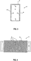
- Figure 4 shows pixel access circuits 54 located on the side of photo detectors 42.
- This arrangement keeps pixel access circuit 54 out of the propagation paths of X-ray radiation 12 from X-ray source 11 and the optical light photons generated in conversion panel 20, thereby benefiting the lifetime of pixel access circuit 54.
- the present invention is not limited to such an arrangement.
- photo detectors 42 are mounted on one side of a substrate and pixel access circuit 54 is located on the other side of the substrate.
- the Substrate protects pixel access circuit 54 from possible damage caused by the X-ray radiation and the optical light photon illumination. This arrangement reduces the physical size of photo detector array 40 without reducing the number of pixels therein.
- the X-ray image acquisition apparatus in accordance with the present invention includes an X-ray conversion panel aligned with a photo detector array.
- the X-ray conversion panel is configured to generate optical light photons in response to the X-ray radiation.
- the conversion panel includes a plurality of conversion cells, each including a conversion body in its core and a light reflective film surrounding the body.
- the conversion body is made of a material that efficiently generates optical light photons in response to X-ray radiation illuminating thereon and is substantially transparent to the optical light photons.
- the conversion bodies are sufficiently long to absorb the X-ray radiation over a wide range of energy levels.
- the light reflective films collimate the optical light photons generated in the conversion bodies.
- the first ends of conversion bodies are covered with an X-ray transparent and light reflective film to increase the efficiency of the conversion panel.
- the photo detector array aligned with the conversion panel is configured to generate electric signals in response to the optical light photons received from the conversion panel.
- Electronic circuits coupled to the photo detector array process the electric signals and generate the images.
- the X-ray image acquisition apparatus is not limited to being used on an imaging system with an X-ray radiation source capable of generating X-rays at different energy levels.
- the X-ray image acquisition apparatus of the present invention can be used on different imaging systems, each system including an X-ray radiation source that is capable of generating X-ray radiation either at a single energy level or at multiple energy levels.
Landscapes
- High Energy & Nuclear Physics (AREA)
- Physics & Mathematics (AREA)
- Health & Medical Sciences (AREA)
- Life Sciences & Earth Sciences (AREA)
- General Physics & Mathematics (AREA)
- Molecular Biology (AREA)
- Spectroscopy & Molecular Physics (AREA)
- Crystallography & Structural Chemistry (AREA)
- Chemical & Material Sciences (AREA)
- Measurement Of Radiation (AREA)
- Apparatus For Radiation Diagnosis (AREA)
- Solid State Image Pick-Up Elements (AREA)
- Transforming Light Signals Into Electric Signals (AREA)
Claims (10)
- Röntgenbilderfassungsvorrichtung (15), die Folgendes umfasst:eine Platte (20); undeine Fotodetektoranordnung (40), die mit der Platte (20) ausgerichtet ist; wobeidie Platte (20) eine Vielzahl von Zellen (22, 30) umfasst, die in einer ersten zweidimensionalen Anordnung angeordnet sind, wobei jede der Zellen (22, 30) konfiguriert ist, um als Reaktion auf eine Röntgenstrahlung optische Lichtphotonen zu erzeugen,jede der Zellen (22, 30) einen Körper (31) einschließt, der aus einem szintillierenden Material besteht, wobei der Körper (31) ein erstes Ende (32), ein zweites Ende (33) und eine Seitenwand (34) aufweist, die sich wenigstens teilweise zwischen dem ersten Ende (32) und dem zweiten Ende (33) erstreckt, wobei jeder der Körper (31) eine Länge aufweist, die wenigstens 1 cm beträgt; wobeidie Fotodetektoranordnung (40) sich unter der Platte (20) befindet, um Licht von dem zweiten Ende von jeder der Zellen zu ermöglichen, die Fotodetektoranordnung (40) zu erreichen;die Fotodetektoranordnung (40) eine zweite zweidimensionale Anordnung von amorphen Siliziumfotodetektoren (42) umfasst, wobei jeder der amorphen Siliziumfotodetektoren (42) konfiguriert ist, um ein Pixel eines Bildes zu bilden;jede der Zellen (22, 30) mit einem oder mehreren der Fotodetektoren (42) ausgerichtet ist, wobei eine Größe der Zellen etwa dieselbe ist wie die der Fotodetektoren, oder größer ist als diese;dadurch gekennzeichnet, dassdas erste Ende (32) von jedem der Körper (31) eine Breite, die irgendwo zwischen 0,05 mm und 0,5 mm liegt, und eine im Wesentlichen quadratische Form aufweist; undjede der Zellen mit einem röntgenstrahltransparenten und lichtreflektierenden Film (38) konfiguriert ist, der das erste Ende (32) des Körpers (31) bedeckt, um eine Effektivität der Platte (20) zu verbessern.
- Röntgenbilderfassungsvorrichtung (15) nach Anspruch 1, wobei jede der Vielzahl von Zellen (22, 30) in der Platte (20) ferner einen lichtreflektierenden Film (36) einschließt, der an der Seitenwand (34) des Körpers (31) befestigt ist.
- Röntgenbilderfassungsvorrichtung (15) nach Anspruch 1, wobei die Vielzahl von Zellen (22, 30) in der Platte (20) auf einen Strahlung emittierenden Punkt einer Röntgenstrahlenquelle (11) fokussiert ist.
- Röntgenbilderfassungsvorrichtung (15) nach Anspruch 1, wobei das szintillierende Material in der Lage ist, eine Röntgenstrahlung bei einem ersten Energieniveau und einem zweiten Energieniveau zu absorbieren, wobei das erste und das zweite Energieniveau Werte sind ausgewählt zwischen 40 keV und 20 MeV, und wobei das szintillierende Material im Wesentlichen transparent für die optischen Lichtphotonen ist.
- Röntgenbilderfassungsvorrichtung (15) nach Anspruch 1, wobei der Körper (31) aus Cäsium-Iod besteht.
- Röntgenbilderfassungsvorrichtung (15) nach Anspruch 1, wobei der Körper (31) aus Wismut-Germanat besteht.
- Röntgenbilderfassungsvorrichtung (15) nach Anspruch 1, wobei der Körper (31) aus Cadmium-Wolframat besteht.
- Röntgenbilderfassungsvorrichtung (15) nach Anspruch 4, wobei die Platte (20) konfiguriert ist, um als Reaktion auf ein Absorbieren von Röntgenstrahlung optische Lichtphotonen zu erzeugen, die einen Spektrumsbereich zwischen infrarot und ultraviolett aufweisen.
- Röntgenbilderfassungsvorrichtung (15) nach Anspruch 1, wobei der Körper (31) einen Umwandlungskörper umfasst, wobei der Umwandlungskörper im Wesentlichen transparent für die optischen Lichtphotonen ist.
- Röntgenbilderfassungsvorrichtung (15) nach Anspruch 2, wobei der lichtreflektierende Film (36) die Seitenwand des Körpers (31) umgibt.
Applications Claiming Priority (3)
| Application Number | Priority Date | Filing Date | Title |
|---|---|---|---|
| US13199 | 2001-11-02 | ||
| US10/013,199 US6800858B1 (en) | 2001-11-02 | 2001-11-02 | X-ray image acquisition apparatus |
| PCT/US2002/034962 WO2003040756A1 (en) | 2001-11-02 | 2002-10-30 | X-ray image acquisition apparatus |
Publications (3)
| Publication Number | Publication Date |
|---|---|
| EP1440332A1 EP1440332A1 (de) | 2004-07-28 |
| EP1440332A4 EP1440332A4 (de) | 2010-11-10 |
| EP1440332B1 true EP1440332B1 (de) | 2018-10-03 |
Family
ID=21758766
Family Applications (1)
| Application Number | Title | Priority Date | Filing Date |
|---|---|---|---|
| EP02802814.0A Expired - Lifetime EP1440332B1 (de) | 2001-11-02 | 2002-10-30 | Röntgenbilderfassungsvorrichtung |
Country Status (4)
| Country | Link |
|---|---|
| US (2) | US6800858B1 (de) |
| EP (1) | EP1440332B1 (de) |
| JP (1) | JP5016180B2 (de) |
| WO (1) | WO2003040756A1 (de) |
Families Citing this family (21)
| Publication number | Priority date | Publication date | Assignee | Title |
|---|---|---|---|---|
| US6800858B1 (en) * | 2001-11-02 | 2004-10-05 | Varian Medical Systems Technologies, Inc. | X-ray image acquisition apparatus |
| US9958569B2 (en) * | 2002-07-23 | 2018-05-01 | Rapiscan Systems, Inc. | Mobile imaging system and method for detection of contraband |
| US7356115B2 (en) * | 2002-12-04 | 2008-04-08 | Varian Medical Systems Technology, Inc. | Radiation scanning units including a movable platform |
| US7672426B2 (en) * | 2002-12-04 | 2010-03-02 | Varian Medical Systems, Inc. | Radiation scanning units with reduced detector requirements |
| US7945021B2 (en) * | 2002-12-18 | 2011-05-17 | Varian Medical Systems, Inc. | Multi-mode cone beam CT radiotherapy simulator and treatment machine with a flat panel imager |
| DE10320862B4 (de) * | 2003-05-09 | 2007-09-06 | Siemens Ag | Verfahren zur automatischen Einstellung einer Blende, sowie Röntgensystem |
| US7015479B2 (en) * | 2003-07-31 | 2006-03-21 | Eastman Kodak Company | Digital film grain |
| US7869862B2 (en) | 2003-10-15 | 2011-01-11 | Varian Medical Systems, Inc. | Systems and methods for functional imaging using contrast-enhanced multiple-energy computed tomography |
| US7649981B2 (en) * | 2003-10-15 | 2010-01-19 | Varian Medical Systems, Inc. | Multi-energy x-ray source |
| US20050082491A1 (en) * | 2003-10-15 | 2005-04-21 | Seppi Edward J. | Multi-energy radiation detector |
| US20070003010A1 (en) | 2005-04-29 | 2007-01-04 | Varian Medical Systems Technologies, Inc. | Radiation systems with imaging capability |
| US7561665B2 (en) * | 2005-10-07 | 2009-07-14 | Varian Medical Systems, Inc. | Dual pulse imaging |
| US7394889B2 (en) | 2006-05-18 | 2008-07-01 | Varian Medical Systems Technologies, Inc. | Contrast-enhanced cone beam X-ray imaging, evaluation, monitoring and treatment delivery |
| WO2008133765A2 (en) | 2007-02-13 | 2008-11-06 | Sentinel Scanning Corporation | Ct scanning and contraband detection |
| US7848488B2 (en) * | 2007-09-10 | 2010-12-07 | Varian Medical Systems, Inc. | Radiation systems having tiltable gantry |
| US20100128839A1 (en) * | 2008-11-21 | 2010-05-27 | Varian Medical Systems, Inc. | Structure and Procedure for X-Ray CT Guided Cancer Treatment |
| US8340245B2 (en) | 2009-06-05 | 2012-12-25 | Sentinel Scanning Corporation | Transportation container inspection system and method |
| US8822932B2 (en) | 2012-01-17 | 2014-09-02 | General Electric Company | Apparatus and system for inspecting structures |
| JP6025456B2 (ja) * | 2012-08-28 | 2016-11-16 | キヤノン株式会社 | 被検体情報取得装置、表示方法、及びプログラム |
| WO2016143401A1 (ja) * | 2015-03-10 | 2016-09-15 | 株式会社島津製作所 | X線検出器 |
| US10806409B2 (en) | 2016-09-23 | 2020-10-20 | Varian Medical Systems International Ag | Medical systems with patient supports |
Citations (2)
| Publication number | Priority date | Publication date | Assignee | Title |
|---|---|---|---|---|
| US5831269A (en) * | 1995-11-29 | 1998-11-03 | Hitachi Metals, Ltd. | Radiation detector element |
| US6114703A (en) * | 1997-10-21 | 2000-09-05 | The Regents Of The University Of California | High resolution scintillation detector with semiconductor readout |
Family Cites Families (26)
| Publication number | Priority date | Publication date | Assignee | Title |
|---|---|---|---|---|
| US4362946A (en) | 1977-11-21 | 1982-12-07 | General Electric Company | Distributed phosphor scintillator structures |
| US4262202A (en) | 1979-08-27 | 1981-04-14 | General Electric Company | Scintillator detector array |
| JPS6243585A (ja) * | 1985-08-21 | 1987-02-25 | Toshiba Corp | X線ct用検出器 |
| US4870667A (en) * | 1985-08-29 | 1989-09-26 | Picker International, Inc. | Radiation detector |
| JPH02291842A (ja) * | 1989-05-02 | 1990-12-03 | Mitsubishi Electric Corp | X線ct装置 |
| US5150394A (en) * | 1989-12-05 | 1992-09-22 | University Of Massachusetts Medical School | Dual-energy system for quantitative radiographic imaging |
| US5187369A (en) * | 1990-10-01 | 1993-02-16 | General Electric Company | High sensitivity, high resolution, solid state x-ray imaging device with barrier layer |
| US5144141A (en) | 1991-08-19 | 1992-09-01 | General Electric Company | Photodetector scintillator radiation imager |
| US5233990A (en) * | 1992-01-13 | 1993-08-10 | Gideon Barnea | Method and apparatus for diagnostic imaging in radiation therapy |
| GB9200828D0 (en) | 1992-01-15 | 1992-03-11 | Image Research Ltd | Improvements in and relating to material identification using x-rays |
| JP3075647B2 (ja) * | 1992-12-25 | 2000-08-14 | 株式会社日立製作所 | X線検査装置の設計方法及びx線検査装置 |
| JPH06289142A (ja) * | 1993-04-05 | 1994-10-18 | Shin Etsu Chem Co Ltd | 放射線検出器およびその製造方法 |
| JPH07148148A (ja) * | 1993-11-29 | 1995-06-13 | Toshiba Corp | X線ct装置用の2次元アレイ型放射線検出器 |
| US5636299A (en) * | 1994-12-28 | 1997-06-03 | Lockheed Missiles & Space Company, Inc. | Hybrid luminescent device and method for imaging penetrating radiation |
| CA2194942A1 (en) * | 1996-01-18 | 1997-07-19 | William P. Novak | Radiation detector with improved response |
| JP3339285B2 (ja) * | 1996-02-02 | 2002-10-28 | 松下電器産業株式会社 | X線撮像装置 |
| US5854684A (en) | 1996-09-26 | 1998-12-29 | Sarnoff Corporation | Massively parallel detection |
| US5956382A (en) * | 1997-09-25 | 1999-09-21 | Eliezer Wiener-Avnear, Doing Business As Laser Electro Optic Application Technology Comp. | X-ray imaging array detector and laser micro-milling method for fabricating array |
| US6236051B1 (en) | 1998-03-27 | 2001-05-22 | Kabushiki Kaisha Toshiba | Semiconductor radiation detector |
| US6429578B1 (en) * | 1999-01-26 | 2002-08-06 | Mats Danielsson | Diagnostic and therapeutic detector system for imaging with low and high energy X-ray and electrons |
| JP2001174564A (ja) * | 1999-12-15 | 2001-06-29 | Ge Yokogawa Medical Systems Ltd | X線検出器およびx線ct装置 |
| WO2001060236A2 (en) * | 2000-02-18 | 2001-08-23 | William Beaumont Hospital | Cone-beam computerized tomography with a flat-panel imager |
| US6553092B1 (en) * | 2000-03-07 | 2003-04-22 | Koninklijke Philips Electronics, N.V. | Multi-layer x-ray detector for diagnostic imaging |
| US6630675B2 (en) * | 2000-07-26 | 2003-10-07 | Siemens Medical Solutions Usa, Inc. | X-ray scintillator compositions for X-ray imaging applications |
| US6487274B2 (en) * | 2001-01-29 | 2002-11-26 | Siemens Medical Solutions Usa, Inc. | X-ray target assembly and radiation therapy systems and methods |
| US6800858B1 (en) * | 2001-11-02 | 2004-10-05 | Varian Medical Systems Technologies, Inc. | X-ray image acquisition apparatus |
-
2001
- 2001-11-02 US US10/013,199 patent/US6800858B1/en not_active Expired - Lifetime
-
2002
- 2002-10-30 JP JP2003542345A patent/JP5016180B2/ja not_active Expired - Fee Related
- 2002-10-30 EP EP02802814.0A patent/EP1440332B1/de not_active Expired - Lifetime
- 2002-10-30 WO PCT/US2002/034962 patent/WO2003040756A1/en not_active Ceased
-
2004
- 2004-10-04 US US10/959,034 patent/US7244943B2/en not_active Expired - Fee Related
Patent Citations (2)
| Publication number | Priority date | Publication date | Assignee | Title |
|---|---|---|---|---|
| US5831269A (en) * | 1995-11-29 | 1998-11-03 | Hitachi Metals, Ltd. | Radiation detector element |
| US6114703A (en) * | 1997-10-21 | 2000-09-05 | The Regents Of The University Of California | High resolution scintillation detector with semiconductor readout |
Also Published As
| Publication number | Publication date |
|---|---|
| US20050045828A1 (en) | 2005-03-03 |
| EP1440332A4 (de) | 2010-11-10 |
| US6800858B1 (en) | 2004-10-05 |
| EP1440332A1 (de) | 2004-07-28 |
| US7244943B2 (en) | 2007-07-17 |
| JP5016180B2 (ja) | 2012-09-05 |
| JP2005508504A (ja) | 2005-03-31 |
| WO2003040756A1 (en) | 2003-05-15 |
Similar Documents
| Publication | Publication Date | Title |
|---|---|---|
| US6800858B1 (en) | X-ray image acquisition apparatus | |
| JP5110784B2 (ja) | 衝撃吸収性カバーを設けたx線検出器 | |
| US7403589B1 (en) | Photon counting CT detector using solid-state photomultiplier and scintillator | |
| US7233640B2 (en) | CT detector having an optical mask layer | |
| CN103760588B (zh) | 光谱ct的检测器阵列 | |
| US20080240341A1 (en) | Hybrid energy discriminating charge integrating ct detector | |
| US20080240339A1 (en) | Energy discriminating detector with direct conversion layer and indirect conversion layer | |
| US7112799B2 (en) | X-ray detector with a plurality of detector units | |
| JP2002528728A (ja) | コンピュータトモグラフ検出器 | |
| US7211801B2 (en) | Radiation detector | |
| CN101254108A (zh) | 轻质坚固的数字x射线探测器 | |
| US20070085015A1 (en) | Lightweight and rugged digital x-ray detector | |
| US11022706B2 (en) | Radiographic detector | |
| EP4076195B1 (de) | Durch aec-rekonfiguration aktivierte intelligente netzverarbeitung | |
| US6989539B2 (en) | Flat dynamic radiation detector | |
| EP1512032B1 (de) | Röntgenstrahlungsdetektor mit einer csi : tl konversionsschicht | |
| EP1948020B1 (de) | Verfahren zur reduzierung von 3d-geistartefakten in einem röntgendetektor | |
| HK1068414B (en) | X-ray image acquisition apparatus | |
| HK1068414A (en) | X-ray image acquisition apparatus | |
| US20220018976A1 (en) | Method and apparatus to improve robustness in a digital radiographic capture device | |
| JP7058998B2 (ja) | 検出器モジュール及びx線ct装置 | |
| EP4403961A2 (de) | Flacher röntgenstrahlendetektor für die computertomographie | |
| JP2019163970A (ja) | シンチレータアレイ、放射線検出器および放射線コンピュータ断層撮影装置 | |
| US20010019600A1 (en) | Planar image detector for electromagnetic rays, particularly X-rays | |
| WO2003092465A2 (en) | Bone densitometry and mammography |
Legal Events
| Date | Code | Title | Description |
|---|---|---|---|
| PUAI | Public reference made under article 153(3) epc to a published international application that has entered the european phase |
Free format text: ORIGINAL CODE: 0009012 |
|
| 17P | Request for examination filed |
Effective date: 20040329 |
|
| AK | Designated contracting states |
Kind code of ref document: A1 Designated state(s): AT BE BG CH CY CZ DE DK EE ES FI FR GB GR IE IT LI LU MC NL PT SE SK TR |
|
| AX | Request for extension of the european patent |
Extension state: AL LT LV MK RO SI |
|
| REG | Reference to a national code |
Ref country code: HK Ref legal event code: DE Ref document number: 1068414 Country of ref document: HK |
|
| RAP1 | Party data changed (applicant data changed or rights of an application transferred) |
Owner name: VARIAN MEDICAL SYSTEMS, INC. |
|
| A4 | Supplementary search report drawn up and despatched |
Effective date: 20101011 |
|
| 17Q | First examination report despatched |
Effective date: 20110516 |
|
| STAA | Information on the status of an ep patent application or granted ep patent |
Free format text: STATUS: EXAMINATION IS IN PROGRESS |
|
| GRAP | Despatch of communication of intention to grant a patent |
Free format text: ORIGINAL CODE: EPIDOSNIGR1 |
|
| STAA | Information on the status of an ep patent application or granted ep patent |
Free format text: STATUS: GRANT OF PATENT IS INTENDED |
|
| INTG | Intention to grant announced |
Effective date: 20180516 |
|
| GRAS | Grant fee paid |
Free format text: ORIGINAL CODE: EPIDOSNIGR3 |
|
| GRAJ | Information related to disapproval of communication of intention to grant by the applicant or resumption of examination proceedings by the epo deleted |
Free format text: ORIGINAL CODE: EPIDOSDIGR1 |
|
| GRAL | Information related to payment of fee for publishing/printing deleted |
Free format text: ORIGINAL CODE: EPIDOSDIGR3 |
|
| STAA | Information on the status of an ep patent application or granted ep patent |
Free format text: STATUS: EXAMINATION IS IN PROGRESS |
|
| GRAR | Information related to intention to grant a patent recorded |
Free format text: ORIGINAL CODE: EPIDOSNIGR71 |
|
| STAA | Information on the status of an ep patent application or granted ep patent |
Free format text: STATUS: GRANT OF PATENT IS INTENDED |
|
| GRAA | (expected) grant |
Free format text: ORIGINAL CODE: 0009210 |
|
| STAA | Information on the status of an ep patent application or granted ep patent |
Free format text: STATUS: THE PATENT HAS BEEN GRANTED |
|
| INTC | Intention to grant announced (deleted) | ||
| INTG | Intention to grant announced |
Effective date: 20180822 |
|
| AK | Designated contracting states |
Kind code of ref document: B1 Designated state(s): AT BE BG CH CY CZ DE DK EE ES FI FR GB GR IE IT LI LU MC NL PT SE SK TR |
|
| REG | Reference to a national code |
Ref country code: GB Ref legal event code: FG4D |
|
| REG | Reference to a national code |
Ref country code: CH Ref legal event code: EP Ref country code: AT Ref legal event code: REF Ref document number: 1049220 Country of ref document: AT Kind code of ref document: T Effective date: 20181015 |
|
| REG | Reference to a national code |
Ref country code: IE Ref legal event code: FG4D Ref country code: DE Ref legal event code: R096 Ref document number: 60249630 Country of ref document: DE |
|
| REG | Reference to a national code |
Ref country code: CH Ref legal event code: PK Free format text: BERICHTIGUNGEN |
|
| REG | Reference to a national code |
Ref country code: NL Ref legal event code: MP Effective date: 20181003 |
|
| RIC2 | Information provided on ipc code assigned after grant |
Ipc: G01T 1/20 20060101AFI20030520BHEP |
|
| REG | Reference to a national code |
Ref country code: AT Ref legal event code: MK05 Ref document number: 1049220 Country of ref document: AT Kind code of ref document: T Effective date: 20181003 |
|
| PG25 | Lapsed in a contracting state [announced via postgrant information from national office to epo] |
Ref country code: NL Free format text: LAPSE BECAUSE OF FAILURE TO SUBMIT A TRANSLATION OF THE DESCRIPTION OR TO PAY THE FEE WITHIN THE PRESCRIBED TIME-LIMIT Effective date: 20181003 |
|
| PG25 | Lapsed in a contracting state [announced via postgrant information from national office to epo] |
Ref country code: ES Free format text: LAPSE BECAUSE OF FAILURE TO SUBMIT A TRANSLATION OF THE DESCRIPTION OR TO PAY THE FEE WITHIN THE PRESCRIBED TIME-LIMIT Effective date: 20181003 Ref country code: BG Free format text: LAPSE BECAUSE OF FAILURE TO SUBMIT A TRANSLATION OF THE DESCRIPTION OR TO PAY THE FEE WITHIN THE PRESCRIBED TIME-LIMIT Effective date: 20190103 Ref country code: CZ Free format text: LAPSE BECAUSE OF FAILURE TO SUBMIT A TRANSLATION OF THE DESCRIPTION OR TO PAY THE FEE WITHIN THE PRESCRIBED TIME-LIMIT Effective date: 20181003 Ref country code: AT Free format text: LAPSE BECAUSE OF FAILURE TO SUBMIT A TRANSLATION OF THE DESCRIPTION OR TO PAY THE FEE WITHIN THE PRESCRIBED TIME-LIMIT Effective date: 20181003 Ref country code: FI Free format text: LAPSE BECAUSE OF FAILURE TO SUBMIT A TRANSLATION OF THE DESCRIPTION OR TO PAY THE FEE WITHIN THE PRESCRIBED TIME-LIMIT Effective date: 20181003 |
|
| PG25 | Lapsed in a contracting state [announced via postgrant information from national office to epo] |
Ref country code: GR Free format text: LAPSE BECAUSE OF FAILURE TO SUBMIT A TRANSLATION OF THE DESCRIPTION OR TO PAY THE FEE WITHIN THE PRESCRIBED TIME-LIMIT Effective date: 20190104 Ref country code: SE Free format text: LAPSE BECAUSE OF FAILURE TO SUBMIT A TRANSLATION OF THE DESCRIPTION OR TO PAY THE FEE WITHIN THE PRESCRIBED TIME-LIMIT Effective date: 20181003 Ref country code: PT Free format text: LAPSE BECAUSE OF FAILURE TO SUBMIT A TRANSLATION OF THE DESCRIPTION OR TO PAY THE FEE WITHIN THE PRESCRIBED TIME-LIMIT Effective date: 20190203 |
|
| REG | Reference to a national code |
Ref country code: CH Ref legal event code: PL |
|
| REG | Reference to a national code |
Ref country code: BE Ref legal event code: MM Effective date: 20181031 |
|
| PG25 | Lapsed in a contracting state [announced via postgrant information from national office to epo] |
Ref country code: LU Free format text: LAPSE BECAUSE OF NON-PAYMENT OF DUE FEES Effective date: 20181030 |
|
| REG | Reference to a national code |
Ref country code: DE Ref legal event code: R097 Ref document number: 60249630 Country of ref document: DE |
|
| REG | Reference to a national code |
Ref country code: IE Ref legal event code: MM4A |
|
| PG25 | Lapsed in a contracting state [announced via postgrant information from national office to epo] |
Ref country code: IT Free format text: LAPSE BECAUSE OF FAILURE TO SUBMIT A TRANSLATION OF THE DESCRIPTION OR TO PAY THE FEE WITHIN THE PRESCRIBED TIME-LIMIT Effective date: 20181003 Ref country code: DK Free format text: LAPSE BECAUSE OF FAILURE TO SUBMIT A TRANSLATION OF THE DESCRIPTION OR TO PAY THE FEE WITHIN THE PRESCRIBED TIME-LIMIT Effective date: 20181003 |
|
| PLBE | No opposition filed within time limit |
Free format text: ORIGINAL CODE: 0009261 |
|
| STAA | Information on the status of an ep patent application or granted ep patent |
Free format text: STATUS: NO OPPOSITION FILED WITHIN TIME LIMIT |
|
| PG25 | Lapsed in a contracting state [announced via postgrant information from national office to epo] |
Ref country code: MC Free format text: LAPSE BECAUSE OF FAILURE TO SUBMIT A TRANSLATION OF THE DESCRIPTION OR TO PAY THE FEE WITHIN THE PRESCRIBED TIME-LIMIT Effective date: 20181003 Ref country code: BE Free format text: LAPSE BECAUSE OF NON-PAYMENT OF DUE FEES Effective date: 20181031 Ref country code: LI Free format text: LAPSE BECAUSE OF NON-PAYMENT OF DUE FEES Effective date: 20181031 Ref country code: SK Free format text: LAPSE BECAUSE OF FAILURE TO SUBMIT A TRANSLATION OF THE DESCRIPTION OR TO PAY THE FEE WITHIN THE PRESCRIBED TIME-LIMIT Effective date: 20181003 Ref country code: CH Free format text: LAPSE BECAUSE OF NON-PAYMENT OF DUE FEES Effective date: 20181031 Ref country code: EE Free format text: LAPSE BECAUSE OF FAILURE TO SUBMIT A TRANSLATION OF THE DESCRIPTION OR TO PAY THE FEE WITHIN THE PRESCRIBED TIME-LIMIT Effective date: 20181003 |
|
| 26N | No opposition filed |
Effective date: 20190704 |
|
| PG25 | Lapsed in a contracting state [announced via postgrant information from national office to epo] |
Ref country code: IE Free format text: LAPSE BECAUSE OF NON-PAYMENT OF DUE FEES Effective date: 20181030 Ref country code: FR Free format text: LAPSE BECAUSE OF NON-PAYMENT OF DUE FEES Effective date: 20181203 |
|
| PGFP | Annual fee paid to national office [announced via postgrant information from national office to epo] |
Ref country code: GB Payment date: 20190923 Year of fee payment: 18 |
|
| PGFP | Annual fee paid to national office [announced via postgrant information from national office to epo] |
Ref country code: DE Payment date: 20190918 Year of fee payment: 18 |
|
| PG25 | Lapsed in a contracting state [announced via postgrant information from national office to epo] |
Ref country code: TR Free format text: LAPSE BECAUSE OF FAILURE TO SUBMIT A TRANSLATION OF THE DESCRIPTION OR TO PAY THE FEE WITHIN THE PRESCRIBED TIME-LIMIT Effective date: 20181003 |
|
| PG25 | Lapsed in a contracting state [announced via postgrant information from national office to epo] |
Ref country code: CY Free format text: LAPSE BECAUSE OF FAILURE TO SUBMIT A TRANSLATION OF THE DESCRIPTION OR TO PAY THE FEE WITHIN THE PRESCRIBED TIME-LIMIT Effective date: 20181003 |
|
| REG | Reference to a national code |
Ref country code: DE Ref legal event code: R119 Ref document number: 60249630 Country of ref document: DE |
|
| GBPC | Gb: european patent ceased through non-payment of renewal fee |
Effective date: 20201030 |
|
| PG25 | Lapsed in a contracting state [announced via postgrant information from national office to epo] |
Ref country code: DE Free format text: LAPSE BECAUSE OF NON-PAYMENT OF DUE FEES Effective date: 20210501 |
|
| PG25 | Lapsed in a contracting state [announced via postgrant information from national office to epo] |
Ref country code: GB Free format text: LAPSE BECAUSE OF NON-PAYMENT OF DUE FEES Effective date: 20201030 |